Note : Les descriptions sont présentées dans la langue officielle dans laquelle elles ont été soumises.
CA 02331813 2000-11-06
SPECIFICATION
Circuit Board of Protective Circuit for Storage Battery, Protective Circuit
Device for Storage Battery, and Storage Battery Pack
Technical Field
The present invention relates to a protective circuit device for a
storage battery for preventing overcharge to the storage battery, circuit
board device of the protective circuit, and storage battery pack provided
with the protective circuit device.
Background Art
In electronic devices such as portable telephones, a storage battery
pack with a storage battery enclosed in a resin casing is generally used as a
power supply source. In most cases, a protective circuit device for
preventing overcharge to the storage battery is included in the storage
battery pack. The protective circuit device has a charging terminal for
charging the storage battery with electricity from a domestic plug socket or
the like, and a discharging terminal for supplying electricity to a terminal
device such as a portable telephone. An exemplary conventional protective
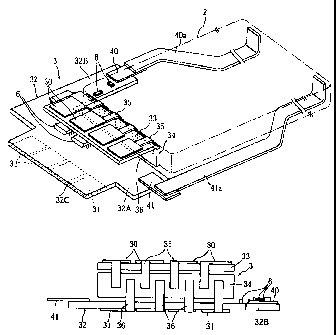
circuit device is shown in Figs. 12 and 13.
A protective circuit device 3 shown in Figs. 12 and 13 has a
prescribed interconnection pattern (not shown) and a circuit board 32 on
which various electronic parts 6, including a chip resistor, are mounted.
Circuit board 32 is in an L shape, and has metal terminals 40 and 41 at
both ends. In addition, a first terminal portion 32C and a second terminal
portion 34A, in which a plurality of metal pieces are inserted into resin, are
mounted to protective circuit device 3. Terminal portions 32C and 34 A
are electrically connected to metal terminals 40 and 41.
First terminal portion 32C has a structure in which the region of the
metal piece is partially exposed from the surface of a resin portion 32c.
First terminal portion 32C is mounted to circuit board 32 such that the
exposed region is on the side of the back surface of circuit board 32 (faces
-1-
CA 02331813 2000-11-06
down). The exposed region turns to, for example, charging terminal 31.
On the other hand, second terminal portion 34A has a structure in which
each metal piece is partially exposed from the upper surface of a so-called
terminal base 34B (a resin portion) having a prescribed height. The region
in which the metal piece is exposed turns to, for example, discharging
terminal 30.
Terminal base 34B has a horizontal portion 34a in which the metal
terminal is exposed, as well as a vertical wall 34c and a plurality of leg
portions 34b that are downwardly extending from horizontal portion 34a.
Namely, with second terminal portion 34A mounted to circuit board 32, a
prescribed space is formed between circuit board 32 and the lower surface of
horizontal portion 34a, as shown in Fig. 13. Thus, various electronic parts
6 can be mounted in the region of circuit board 32 directly below horizontal
portion 34a before mounting second terminal portion 34A. After mounting
electronic parts 6, second terminal portion 34A is mounted to circuit board
32 such that contact between second terminal portion 34A and electronic
parts 6 is avoided.
However, the above described protective circuit device 3 suffers from
problems related to a low efficiency in manufacture and cost involved. The
reason is as follows. Since first and second terminal portions 32C and 34A
are formed by inserting metal pieces into resin, steps of forming terminal
portions 32C and 34A are additionally required. Further, in the steps of
forming terminal portions 32C and 34A, molds for forming resin portions
32c and 34B of terminal portions 32C and 34A and for inserting the metal
pieces are required. The molds are required for each of terminal portions
32C and 34A.
Moreover, manufactured protective circuit device 3 should be tested
to determine as to if it operates as designed. Then, if protective circuit
device 3 is determined to be defective due to a mounting failure of electronic
part 6 mounted in a region of circuit board 3 corresponding to second
terminal portion 34A, such poorly mounted electronic part 6 cannot be re-
mounted unless second terminal portion 34A is removed. Thus, if
electronic part 6 is not properly mounted in the region of circuit board 32
-2-
CA 02331813 2000-11-06
English Translation of Annexes
corresponding to second terminal portion 34A, protective circuit device 3
must be discarded, whereby the yield is decreased.
Disclosure of the Invention
The present invention is made to solve the aforementioned problems.
An object of the present invention is to manufacture a protective circuit
device and storage battery pack with high efficiency and favorable cost.
A circuit board of a protective circuit for a storage battery according
to the present invention has a first board including a circuit portion, and a
second board connected to the first board through a plate-like deformable
metal member. The circuit portion includes, for example, an
interconnection pattern and an electronic part connected thereto. The
conductive material may be a metal piece, for example.
The first board preferably has a first external terminal electrically
connected to the circuit portion. The second board preferably has a second
external terminal electrically connected to the circuit portion.
Further, the first board preferably has a protrusion protruding from
one end thereof. In this case, the first external terminal is formed on the
protrusion. The second board is preferably arranged on the side opposite
to the protrusion with respect to and spaced from the first board.
A third board may be provided between the first and second boards.
In this case, the first, second, and third boards may be connected by the
same conductive member. The conductive member may include the first
and second conductive members. Then, the first conductive member
connects the first and third boards, whereas the second conductive member
connects the second and third boards.
Further, the first and second boards may be formed in the region
surrounded by a frame. A plurality of such regions are provided, each
having the first and second boards.
Normally, various electronic parts and the like are mounted on the
board with a plurality of boards collectively connected by the frame. After
terminals to be electrically connected to the mounted electronic parts are
formed, each board is separated from the frame. Thus, a circuit for an
-3-
CA 02331813 2000-11-06
intended use is obtained. Here, as the second board (island) is connected
to the first board (the circuit board body) through the conductive member,
the second and the first boards are maintained in a desired positional
relationship with the conductive member bent. For example, the second
board can be vertical or parallel to the first board. In addition, if the
circuit board of the protective circuit has a third board (island), for
example,
the second board can be parallel to the first board and the third board can
be vertical to the first board thereby connecting the first and second boards.
Since the second board is connected to the first board through the
conductive member, the second and first boards can be electrically
connected. In this case, the second board may be provided with electronic
parts and terminals. If the protective circuit board is provided with a third
board, the second board can be parallel to the first board by separating the
board from the frame and bending the conductive member. Thus, if the
external terminal is formed on the second board, for example, the above
mentioned second and third boards serve as the second terminal portion of
the conventional example.
If the second board is parallel to the first board and the second board
is arranged directly above the first board, a prescribed space is obtained
between the first and second boards. The height of the space can be
determined by appropriately selecting the dimension of the third board,
length of the conductive member and the like. Various electronic parts are
mounted to the first board before bending the conductive member, for
example in the state of collective board. In this case, by appropriately
setting the height of the space, contact between the second board and the
electronic parts can be avoided even if the second board is arranged directly
above the first board after the electronic parts are mounted. In addition,
at least the thickness of the storage battery ensures the thickness of the
protective circuit device (a distance between the second and first boards).
Accordingly, the electronic parts can also be mounted on opposing surfaces
of the first and second boards, whereby the mounting area of the electronic
parts can be increased.
The circuit board of each protective circuit can be tested as to if it
-4-
CA 02331813 2000-11-06
operates as intended in the state of the collective board with the protective
circuit board supported by the frame. Since the test is performed with the
second terminal portion formed, if the electronic parts are not properly
mounted below the horizontal portion of the second terminal portion, it is
difficult to re-mount the electronic parts. On the other hand, in the
present invention, test is performed with the first and second boards being
flush with each other in the state of the collective board, i.e., with the
electronic parts being mounted. Thus, if the test reveals that the
electronic part is poorly mounted, such an electronic part can easily be re-
mounted, so that the yield increases. Further, as the first and second
external terminals are respectively formed on the first and second boards in
the state of collective board, an amount of displacement in position between
the external terminals after the manufacture of the protective circuit device
can be reduced as compared with the conventional example where the
external terminal portion is separately mounted to the board.
A protective circuit device for a storage battery according to the
present invention includes a first board having a circuit portion, and a
second board connected to the first board through a plate-like metal
member.
The first board preferably has a first external terminal electrically
connected to the circuit portion, and the second board preferably has a
second external terminal electrically connected to the circuit portion.
The conductive member is preferably bent, and the second board is
arranged opposite to and spaced from the first board.
The first board may have a protrusion. In this case, the first
external terminal is formed on the protrusion. The second board is
connected to the end of the first board positioned on the side opposite to the
protrusion.
Electronic parts electrically connected to the circuit portion may be
mounted on the surface of the second board that is opposite to the first
board.
Further, a third board may be provided between the second and first
boards. In this case, the third board may be vertical to the first board and
may have an interconnection pattern electrically connected to the circuit.
-5-
CA 02331813 2000-11-06
portion on the surface of the third board.
An electronic part without a coating for increasing moisture
resistance may be mounted on the second board, and that with such a
coating may be mounted on the first board.
According to the protective circuit device for a storage battery of the
present invention, the second board can be vertical to or parallel to the
first
board by bending the conductive member. Thus, the protective circuit
device can be conveniently incorporated in the storage battery pack.
Some protective circuit devices are coated with epoxy or acrylic based
resin, and the like. Although the coating operation is performed on a
specific electronic part, in this case, the electronic parts not to be coated
should be masked with a polyimide tape or the like. In the protective
circuit device of the present invention, the first and second boards are
connected through the conductive member, but the mounting surfaces of the
electronic parts of the boards are separated. Thus, the electronic parts
without coatings are concentrated on the second board, and those with
coatings are concentrated on the first board, so that the coating operation
can be intensively performed on the first board. As a result, the electronic
parts not to be coated, i.e., those mounted to the second board, needs not be
masked. Thus, in the protective circuit of the present invention, an
operation of coating the electronic parts with resin is not only facilitated,
but a masking operation for coating can advantageously be eliminated.
In addition, when the third board is provided, the second board is
parallel to the first board, and the third board is vertically connected to
the
first and second boards, a terminal base of the conventional protective
circuit device can be formed by the second and third board. Here,
formation of the external terminal on the second board enables formation of
a portion corresponding to the conventional second terminal portion by the
second and third board as well as the external terminal. Thus, the second
terminal portion needs not be separately formed by insertion, so that
manufacturing efficiency of the protective circuit device is increased and
cost is reduced.
A protective circuit device according to the present invention can be
-6-
CA 02331813 2000-11-06
obtained by directly forming the external terminal on the protective circuit
board in the state of collective board, for example, and by bending the
conductive member after separating the protective circuit board from the
collective board. A series of the above described operations enables
formation of the portion corresponding to the second terminal portion of the
conventional protective circuit device. Accordingly, there is no need to
mount the second terminal portion to the first board. In addition, since
the portion corresponding to the second terminal portion needs not be
formed by resin molding, there is no need to prepare a mold. Thus, cost
involved is extremely favorable.
In addition, a plurality of external terminals to be electrically
connected to the interconnection pattern can be directly formed. Namely,
the portion corresponding to the first terminal portion of the conventional
protective circuit device can directly be formed in the first board. In this
case also, manufacturing efficiency of the protective circuit device is
increased and cost is reduced. Although the first terminal portion is also
formed by insertion as in the case of the second terminal portion, which is
in turn mounted to the protective circuit board such an operation is not
necessary in the convention protective circuit device.
It is noted that each external terminal portion may be formed by
mounting a terminal such as metal, or by coating a terminal pad, which is
formed simultaneously with the interconnection pattern, with metal.
A storage battery pack of the present invention includes a storage
battery, a protective circuit device electrically connected to the storage
battery to prevent overcharge to the storage battery, and an insulation
casing enclosing the storage battery and the protective circuit device. The
protective circuit device includes a first board having a circuit portion, and
a second board connected to the first board through a plate-like metal
member.
The conductive member is preferably bent. At the time, the second
board is preferably arranged in a position opposite to and spaced from the
first board. The second board has a second external terminal electrically
connected to the circuit portion. The first board preferably has a first
external terminal electrically connected to the circuit portion. The first
- 7-
CA 02331813 2000-11-06
and second external terminals are exposed from the surface of the
insulation casing.
A storage battery may be inserted between the second and first
boards.
The storage battery pack of the present invention is provided with
the above described protective circuit device, so that aforementioned
various effects are produced. Therefore, the storage battery pack of high
performance can be provided with low cost.
Brief Description of the Drawings
Fig. 1 is a perspective view showing an exemplary storage battery
pack according to the present invention.
Fig. 2 is a side view showing a protective circuit device incorporated
in the storage battery pack shown in Fig. 1.
Fig. 3 is a perspective view showing the protective circuit device.
Fig. 4 is a back view showing the protective circuit device.
Fig. 5 is a perspective view showing a collective board used for
manufacturing the protective circuit device.
Fig. 6 is a perspective view showing a unit circuit board (protective
circuit) on which various electronic parts are mounted in the first mounting
step.
Fig. 7 is a perspective view showing a unit circuit board (protective
circuit) on which various electronic parts are mounted in the second
mounting step.
Fig. 8 is a perspective view showing the unit circuit board separated
from the collective board.
Fig. 9 is a perspective view showing a modification of the protective
circuit device.
Fig. 10 is a perspective view showing another modification of the
protective circuit device.
Fig. 11 is a perspective view showing another embodiment of the
protective circuit device according to the present invention.
Fig. 12 is a perspective view showing an exemplary conventional
-8-
CA 02331813 2000-11-06
protective circuit device.
Fig. 13 is a back view showing a conventional protective circuit
device.
Best Modes for Carrying Out the Invention
Now, preferred embodiments of the present invention will be
described in detail with reference to the drawings.
Fig. 1 is a perspective view showing an exemplary storage battery
pack according to the present invention. Fig. 2 is a perspective side view
showing a protective circuit device according to the present invention which
is incorporated in the storage battery pack. Fig. 3 is a perspective view of
the protective circuit device. Fig. 4 is a back view of the protective circuit
device. It is noted that, the same members, elements and the like shown
in the drawings are denoted by the same reference numerals as in the
conventional example. In addition, in the present embodiment, the
storage battery pack used as a power supply source for a portable telephone
is described.
As shown in Figs. 1 and 2, a storage battery pack 1 has a structure in
which a storage battery 2 and protective circuit device 3 are enclosed in a
resin casing 10, which is generally rectangular in shape when viewed from
above and has a prescribed thickness. Four discharging terminals 30 for
supplying electricity from storage battery 2 to a portable telephone body
(not shown) are formed on one surface 10a of storage battery pack 1. Four
charging terminals 31 for charging storage battery 2 with electricity from
the external power supply source (not shown) are exposed on the other
surface lOb of storage battery pack 1.
Discharging terminal 30 and charging terminal 31 are formed on
protective circuit device 3. Protective circuit device 3 has a circuit board
body (first board) 32, first island (second board) 33, and second island
(third
board) 34, as shown in Figs. 2 and 4. The material and thickness of these
portions are substantially the same.
As shown in Fig. 3, circuit board body 32 is in an L shape, where a
narrow portion 32B extends from one side of a wide portion 32A in a width
-9-
CA 02331813 2000-11-06
direction at the end of the wide portion 32A. In addition, circuit board
body 32 has an extending portion (protrusion) 32C outwardly extending
from one side of wide portion 32A from the middle portion thereof. Circuit
board body 32 in such a configuration is provided, on its front and back
surfaces, with prescribed patterns (not shown) forming a part of the circuit
portion. Various electronic parts 6 such as a chip resistor are mounted to
the front surface (in some cases also to the back surface) of circuit board
body 32 to be electrically connected to the interconnection patterns and to
form the part of the circuit portion. Metal terminals 40 and 41 such as
nickel plates are mounted to both ends of circuit board body 32 (leading
ends of wide portion 32A and narrow portion 32B). Terminals 40a, 41a for
extension are connected to metal terminals 40 and 41, which are in contact
with the electrode of storage battery 2.
Four first external terminals 31 are formed on the back surface of
protrusion 32C to be electrically connected to the interconnection patterns.
Namely, a portion corresponding to the first terminal portion of the
conventional protective circuit device is formed by protrusion 32C and each
of the first external terminals 31. It is noted that these first external
terminals 31 are fornied by mounting the terminals such as metal by means
of soldering or by coating the terminal pad with metal which is formed
simultaneously with the interconnection patterns. When protective circuit
device 3 is included in a prescribed casing to form storage battery pack 1,
each of first external terminals 31 turns to charging terminal 31 for
supplying storage battery 2 with electricity from the external power supply
source (not shown).
As shown in Fig. 3, first island 33 is rectangular in shape and
arranged parallel to and above wide portion 32A. First island 33 is
connected to circuit board body 32 through second island 34 which is
vertically arranged between first island 33 and circuit board body 32.
More specifically, as shown in Figs. 2 and 4, first island 33 and second
island 34 are connected by four first metal pieces (conductive members) 35,
each bent at a right angle. Second island 34 and circuit board body 32 are
connected by four second metal pieces (conductive members) 36, each bent
-10-
CA 02331813 2000-11-06
at an right angle. As in the case of first external terminals 31, these
second external terminals 30 are formed by mounting terminals such as
metal or by coating the external pad which is formed simultaneously with
the interconnection pattern with metal.
Each of first metal piece 35 is electrically connected to corresponding
second external terminal 30 and, for example, is electrically connected to
corresponding second metal piece 36 by an interconnection formed on
second island 34. These second metal pieces 36 are electrically connected
to the interconnection pattern formed on circuit board body 32, so that each
second external terminal 30 is electrically connected to the interconnection
pattern. The back surface of first island 33 may be provided with a
prescribed interconnection pattern and electronic parts 6. It is noted that,
when protective circuit device 3 is enclosed in a prescribed casing to form
storage battery pack 1, each of second external terminals 30 turns to
discharging terminal 30 for supplying the portable telephone body (not
shown) with electricity.
In protective circuit device 3 having the above described structure,
second external terminal 30 is formed on first island 33 which is arranged
parallel with circuit board body 32 at a prescribed height. Thus, first
island 33, second island 34, and second external terminal 30 form a portion
corresponding to the second terminal portion of the conventional protective
device.
Next, a manufacturing method of protective circuit device 3 will
briefly be described. For the sake of convenience, first, description of a
collective board 7 used in manufacturing protective circuit device 3 will be
given with reference to Fig. 5. It is noted that, in the present embodiment,
first and second external terminals 30, 31 are formed by mounting metal
terminals.
As shown in Fig. 5, collective board 7 has a plurality of rectangular
regions surrounded by frame 70. Each of the rectangular regions has a
unit circuit board (corresponding to circuit board body 32, first island 33,
and second island 34). In collective board 7, circuit board body 32, first
island 33, and second island 34 of protective circuit device 3 are separated
-11-
CA 02331813 2000-11-06
when viewed from above. Circuit board body 32 is supported by frame 70
through bridges 71. Circuit board body 32 is also connected to second
island 34 through bridges 71. First island 33 is also supported by frame
70 through bridges 71. First island 33 is also connected to second island
34 through bridges 71.
Various electronic parts and metal pieces must be mounted onto both
surfaces of collective board 7, so that the mounting operation must be
performed twice. In this case, the first mounting operation is performed as
follows. Namely, various electronic parts 6 and metal pieces are
automatically aligned and positioned using a mounter or the like,
corresponding to prescribed terminal pads formed on circuit board body 32.
Thus, the structure as shown in Fig. 6 is obtained. A solder paste is
preliminary applied to the terminal pad or the terminal of the part to be
mounted. The solder paste is re-melted in a furnace for reflowing, and
cooled down to solidify. Thus, electronic parts 6 and the like are mounted.
Then, the second mounting operation is performed. The operation is
performed with the front and back surfaces of collective board 7 reversed.
More specifically, each of first metal pieces 35 is placed over first island
33
and second island 34 to connect them, and each of second metal pieces 36 is
placed over second island 34 and circuit board body 32 to connect them.
This results in the structure shown in Fig. 7. In the present embodiment,
since external terminals 30 and 31 are formed by metal terminals, metal
terminals are arranged on first island 33 and protrusion 32 of circuit board
body 32. A solder paste is preliminary applied to each of metal pieces 35
and 36 and metal terminals or the terminal pad provided with the terminal
pieces. The solder paste is re-melted in the reflow furnace, and then cooled
down to solidify. Thus, each of metal pieces 35 and 36, metal terminals
and the like are mounted.
A given circuit such as protective circuit device 3 is in some cases
coated for example with epoxy or acrylic based resin for preventing leakage.
The coating operation is performed on a specific electronic part 6. During
the coating operation, electronic part 6 that is not to be coated is masked by
a polyimide tape or the like. Although circuit board body 32 and first
-12-
CA 02331813 2000-11-06
island 33 are connected through metal pieces 35, 36 in collective board 7,
mounting surfaces of electronic parts 6 of circuit board body 32 and first
island portion 33 are separated when viewed from above. Thus, electronic
parts 6 which are not to be coated are concentrated for example on first
island 33 and those to be coated are concentrated on circuit board body 32,
so that an intensive coating operation on circuit board body 32 is
facilitated.
In addition, a masking operation on electronic part 6 which is not to be
coated, i.e., electronic part 6 mounted on first island 33, can be eliminated.
Thus, when protective circuit device 3 is manufactured using collective
board 7, a masking step for coating electronic part 6 with resin can
advantageously be eliminated.
Each unit circuit board provided with electronic part 6 or the like as
described above substantially operates in the same way as protective circuit
device 3, so that each unit circuit board (circuit) is tested to determine as
to
if it operates as intended in the state of collective board 7. In the
conventional example, the test is performed with the second terminal
portion formed. Thus, if electronic part 6 below the horizontal portion of
the second terminal portion is poorly mounted, it is difficult to re-mount the
electronic part. On the other hand, in the present invention, test is
performed in the state of collective board 7, i.e., the state in which
electronic part 6 is mounted. Accordingly, even if it is determined that
electronic part 6 and the like are poorly mounted, such electronic parts can
be re-mounted, so as to increase the yield .
Then, by cutting bridges 71, protective circuit device 3 shown in Fig.
8 is obtained. In protective circuit device 3 in this state, first island 33
and
second island 34 are separated from circuit board body 32. More
specifically, first and second islands 33 and 34 are spaced apart from circuit
board body 32 in a horizontal direction. First and second metal pieces 35,
36 of protective circuit device 3 in this state are bent as shown by an
imaginary line in Fig. 8. Thus, protective circuit device 3 shown in Fig. 2
or Fig. 4 is obtained.
As described above, a series of operations of mounting various
electronic parts 6 and the like in the state of collective board 7 and bending
-13-
CA 02331813 2000-11-06
metal pieces 35, 36 provides portions corresponding the first and second
terminal portions of the conventional protective circuit device. Thus, there
is no need to form the first and second terminal portions by insertion
molding and to mount them to circuit board body 32. Particularly, molds
need not be prepared since resin is not necessary, so that cost is favorably
reduced. Further, the alignment accuracy of the first and second external
terminals can be increased as compared with the conventional example.
Moreover, if metal pieces 35, 36 are bent, first island 33 is arranged
parallel to circuit board body 32, and first island 33 is arranged directly
above circuit board body 32, a prescribed space is formed between circuit
board body 32 and first island 33 as shown in Figs. 2 and 3. The height of
the space can be suitably determined for example by a dimension of second
island 34, length of each of metal pieces 35, 36, and the like. Various
electronic parts 6 are mounted to circuit board body in the state of
collective
board 7 before bending metal pieces 35 and 36. In this case, as long as the
height of the space is properly set, even if metal pieces 35, 36 are bent and
first island 33 is arranged directly above circuit board body 32 after
mounting electronic part 6, contact between first island 33 and electronic
part 6 is avoided. In addition, if circuit board body 32 is used as protective
circuit device 3 for a storage battery, the thickness of protective circuit
device 3 (a distance between first island 33 and circuit board body 32) can
be at least the thickness of the storage battery. Accordingly, electronic
parts 6 can be mounted on opposing surfaces of circuit board body 32 and
first island 33, so that the mounting area of electronic parts 6 can be
increased.
It is noted that, in the above described embodiment, first island 33
and second island 34 are connected by first metal piece 35, and second
island 34 and circuit board body 32 are connected by second metal piece 36.
However, as shown in Fig. 9, first island 33, second island 34, and circuit
board body 32 may be coniiected by one kind of metal piece 35A as shown in
Fig. 9.
Further, second island 34 may be eliminated. Namely, as shown in
Fig. 10, protective circuit device 3 may have only first island 33.
-14-
CA 02331813 2000-11-06
Then, another embodiment of the present invention will be described
with reference to Fig. 11. It is noted that the same members or
components are denoted by the same reference numerals as in the
aforementioned embodiment, and therefore description thereof will not be
repeated.
The structure of protective circuit device 3 of the present embodiment
is basically the same as that of protective circuit device 3 of the above
described embodiment. Protective circuit device 3 is different from that of
the above described embodiment in first island 33 and second island 34.
In other words, in the above described embodiment, first and second islands
33 and 34 are formed continuously from one side of circuit board body 32 in
the width direction (direction in which narrow portion 32B protrudes).
However, in the present embodiment, first and second island 33 and 34 are
formed continuously from the other side of circuit board body 32 in the
width direction.
In the structure, an opening is formed on one side of circuit board
body 32 in the width direction by first and second islands 33 and 34. Thus,
if electronic parts 6 and the like are not mounted on the bottom side of first
island 33 and directly below first island 33, the end of storage battery 2 can
be enclosed in the space. Consequently, a storage battery pack with the
above described protective circuit device 3 can be reduced in dimension in a
longitudinal direction.
Although the present invention has been described, it is clearly
understood that the same is by way of illustration and example only in all
respects and is not to be taken by way of limitation. The scope of the
present invention is limited by the terms of the appended claims, which
includes meanings equivalent to the scope of the claims and all alterations
in the scope.
Industrial Applicability
The present invention is effectively applied to a protective circuit for
a storage batter and a storage battery provided with the same.
-15-