Note : Les descriptions sont présentées dans la langue officielle dans laquelle elles ont été soumises.
CA 02331992 2001-O1-22
A. Bond 5
HIGH SPEED SEMICONDUCTOR PHO'TODETECTOR
held of the Invention
This invention relates to semiconductor photodetectors, and in particular to
Avalanche Photodetectors.
Background of the Invention
Optoelectronic devices are now receiving a great deal of attention for use in
telecommunications networks primarily for their huge information handling
capacity
An integral part of the network is the semiconductor pho~todetector which
converts
incident light to an electrical signal. A standard type of photodetector is
the PIN diode
which includes an intrinsic semiconductor light-absorbing layer sandwiched
between
n-type and p-type semiconductor layers. One of the problems associated with
such a
device is that the relatively thick intrinsic layer (usually 200 - 400 nm)
limits the
transit time of electrons and holes generated by the incident light and
therefore limits
the speed of the device. Recently, it has been proposed to reduce the
intrinsic layer
thickness and sandwich it between two waveguide layers in order to increase
the
absorption length. Such a device still suffers from transit time limitations,
since the
intrinsic region, which is defined as the region including an electric field
when a bias
is supplied to the device, includes the thickness of the waveguide layers. It
has also
been suggested that light could be coupled to the intrinsic region of a
standard PIN
device by means of a waveguide.
Another type of photodetector is the waveguide avalanche photodetector. This
type of device usually includes, as part of the intrinsic layer, an undoped
absorbing
and waveguide layer, a doped charge layer, and an undoped multiplication
layer.
Again, such devices have a fairly thick intrinsic layer, usually of the order
of 700 to
1000 nm, which limits transit times.
It is desirable, therefore, to provide a photodetector which exhibits fast
transit
times so that the device can be operated at high speeds.
Summary of the Invention
The invention in one aspect is a semiconductor avalanche photodetector which
includes an essentially undoped multiplication layer, a thin, substantially
undoped
light absorbing layer, and a doped waveguide layer which is separate from the
light
absorbing layer and is capable of coupling incident light into the light
absorbing layer.
1
CA 02331992 2001-O1-22
A. Bond 5
In other aspects the invention is a method of fabricating m avalanche
photodetector
and a network and receiver including an avalanche photodetector.
Brief Description of the F~eures
These and other features of the invention axe delineated in detail in the
following description. In the drawing:
Fig 1 is a cross sectional view of an avalanche pht:otodetector in accordance
with an embodiment of the invention;
Fig 2 is a top view of the device of Fig l; and
Fig. 3 is a schematic drawing of a portion of a network including the device
of
Figs. 1 and 2.
It will be appreciated that, for purposes of illustraxion, these figures are
not
necessarily drawn to scale.
Detailed Description
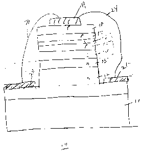
A typical device made in accordance with the invention is illustrated in Figs
1
and 2. It will be appreciated that in the cross sectional view of Fig l, light
(represented by the arrow in Fig 2) would be incident on. an edge of the
device from
the viewer into the page of the figure. The invention in accordance with this
embodiment is a semiconductor avalanche photodetecto:r, 10, which includes an
essentially undoped multiplication layer, 14, a thin, substantially undoped
light
absorbing layer, 16, and a doped waveguide layer, 17, which is separate from
the light
absorbing layer and is capable of coupling incident light: usually into the
light
absorbing layer.
In more detail, the device, 10, is usually formed on a semiconductor
substrate,
11, which, in this case, is preferably semi-insulating InF'. Formed on the
substrate by
standaxd techniques, such as Metal Organic Chemical Vapor Deposition (MOCVD),
or other well known techniques, are a succession of epit:axial semiconductor
layers, 12
- 18. The first layer is a cladding layer, 12, which is preferably n-type InP
material
which typically has a thickness of 400-1000 nm and is doped to an exemplary
concentration of about 2 x 1018 cm 3. Formed on the cladding layer, 12, is an
n-doped
charge layer, 13, which in this example is InAIAs. This layer is typically 200
nm thick
and is doped to an exemplary concentration of 2 x 10'$ cni 3 so as to
substantially
prevent tunneling of charge caxriers into the cladding layer and substrate. It
will be
2
CA 02331992 2001-O1-22
A. Bond 5
appreciated that, although use of the charge layer, 13; an~i cladding layer,
12, are
preferable, they are not essential to the invention.
Formed on the charge layer, 13, is a multiplication layer, 14, which is
substantially undoped (intrinsic). It should be appreciated that "undoped" in
the
context of the application means not intentionally doped, and the layer could
include
some small amount of background doping (less than 1 x 10" cm 3) of n or p-type
dopants. In this example, the layer; 14, comprises InAlA~s, but could be any
semiconductor material which provides multiplication of free carriers
generated in the
device in response to incident light, such as InP. The thickness of the layer,
14 is
typically in the range 200 to 1000 nm. A second charge payer, 15, is
preferably formed
on the multiplication layer, 14. This layer is preferably doped with p-
conductivity
type impurities to a concentration within the range 7 x 101 to 2 x 101$ cni 3.
In this
example, the layer, 15, comprises InAlAs with a preferrf;d thickness in the
range 50 -
100 nm and serves to shield the absorber layer, to be described, from the high
ele~.ctric
fields generated in the multiplication layer during the oF~eration of the
device. Other
suitable materials include InP.
A thin, substantially undoped absorbing layer, 1~5, is formed on the charge
layer, 15. In this example, the layer, 16, comprises InGa.As, but could be any
semiconductor material which absorbs incident light an<i generates free
carriers in
response thereto. The thickness of this layer is desirably in the range 50 -
i00 nm.
Formed on the absorbing layer, 16, is a transparent waveguide, 17. The
waveguide layer is preferably doped with p-conductivity type impurities to a
concentration within the range 7 x 101' to 1 x 10¹⁸ crn'. In this example the
waveguide layer preferably comprises InGaAsP but could be any other material
which
has a higher index of refraction than; and is lattice matched to, the cladding
layer, 18,
to be described. The thickness of the waveguide layer is preferably 200 - 400
nm.
Finally, a p-type doped cladding layer, 18, is formed over the waveguide
layer;
17. The layer, 18, in this example comprises InP, but could be any material
that has a
lower index of refraction than the waveguide layer. The; thickness of the
cladding
layer, 18, is typically within the range 1000 - 2000 nm" Electrical contact to
the
cladding layer, 18, is provided by metal layer 19 on the, cladding layer, and
metal
layers 20 and 21 on the n-cladding layer, 12. Contact ribbons, 23 and 24,
electrically
connect metal layer, 19, to metal layers 20 and 21. As illustrated in Fig 2,
electrical
contact to n-type cladding layer, 13, is provided by metal layer, 22, formed
on an
etched step of the device exposing the cladding layer, ~~3. The metal layers,
19-22
3
CA 02331992 2001-O1-22
A. Bond 5
could be gold alloys or any other conductive material whiich forms an ohmic
contact
to the semiconductor material. It will be appreciated that this contacting
scheme is
only one of many possible techniques which could be employed to contact the
device.
In operation, and as understood; a reverse bias is supplied to the device
through contacts, 20-22 while light propogates through the waveguide layer,
17, in the
direction into the page of Fig 1. The light couples to the absorber layer, 16,
as it
moves along the waveguide layer, 17, resulting in the generation of free
carriers
(electrons and holes) in the absorbing layer. These carriers are swept out of
the
absorbing layer, 16, by the applied electric field, and the electrons multiply
by impact
ionization in the multiplication layer; 14. This increase vi electrons is
detectable by
circuitry (not shown) connected to the contacts, 20-22. la is understood that
other
additional or alternative mechanisms may occur as well.
Fig. 3 illustrates a portion of a typical optical network which may employ the
device, 10, previously described. A transmitter, 30, which preferably includes
a
semiconductor laser (not shown) transmits light of one or more wavelengths
over an
optical fiber 31. The fiber, 31, couples the light to an optical receiver, 32,
which
includes the avalanche photodetector, 10. Current generated by the
photodetector, l0,
in response to the light is preferably electrically coupled to a
transimpedance
amplifier, 33, which amplifies the electrical signal and converts the current
to a
voltage signal which is coupled as the data signal to the rest of the receiver
and other
portions of the network.
It will be appreciated that some of the advantages of the present indention
may
reside in the separation of the waveguide layer, 17 from the absorber layer,
16. That
is, since the waveguide layer is now a sepaxate, doped layer, there is no
substantial
electric field across the layer and it is no longer part of the intrinsic
region of the
device. Instead, the intrinsic region comprises layers 14.-16. This means that
the
intrinsic layer thickness can be reduced to a typical vah~e of 300 - 500 nm.
This, in
turn, reduces the transit time of the carriers resulting in faster devices.
For example, in
a typical prior art APD, the absorption and waveguide layer is at least 350 nm
for
efficient waveguiding, the charge layer is about 50 nm, and the multiplication
layer is
about 200 nm, giving an intrinsic region thickness of approx. 600 nm. The
transit time
limited bandwidth, which is inversely proportional to tlhe thickness of the
intrinsic
region, in such a device would be approximately 38 GHz. In an example of the
present invention, the thickness of the absorbing layer, 16, is reduced to 50
nm, and
3S the intrinsic layer thickness (layers 14-16) is reduced to 300 nm. This
gives a transit
time limited bandwidth of approx. 76.6 GHz. Desirably, the transit time
limited
4
CA 02331992 2001-O1-22
A. Bond 5
bandwidth is at least 40 GHz. In addition, the power handling of such a device
is
increased by a factor of 25 due to the distributed absorption of light over
the first 50
microns of the absorber layer as opposed to absorption of the light in the
first few
microns of the thicker waveguide absorber layer in the prior art example
above.
Finally, the separation of the waveguide and absorption Layers permits
tailoring
absorption properties independent of waveguide design considerations.
5