Note : Les descriptions sont présentées dans la langue officielle dans laquelle elles ont été soumises.
CA 02333684 2000-12-01
WO 99/63650 PCT/US99/12237
SOLID STATE TRANSFORMER
FIELD OF THE INVENTION
The present invention relates generally to
electrical transformers, and more particularly to a solid
state distribution transformer.
BACKGROUND OF THE INVENTION
Distribution transformers range widely in power
delivery capability and physical size. Ratings are as small
as 1.5 kVA and as large as 500 kVA or up to 'small power,
ratings of 2500 or 3000 kVA. The function of a distribution
transformer is to reduce voltage on the medium utility
system of from 2400 to 35000 down to utilization voltages of
from 120 to 600 volts.
Transformers may be single phase devices or may be
three phase devices, or may consist of single phase devices
interconnected to supply three phase power. Distribution
transformers can be oil-immersed, to provide better
insulation and cooling or may be "dry-types" which are air-
cooled, but will therefore be physically larger and require
more weather protection than sealed, oil-immersed
transformers.
Transformers generally contain two or more
electrical circuits, primary and secondary windings,
consisting of multiturn coils of electrical conductors that
are interlinked by means of one or more magnetic circuits or
cores. Cores typically consist of a plurality of
CA 02333684 2000-12-01
WO 99/63650 PCT/US99/12237
- 2 -
ferromagnetic laminations that are stacked together to form
a closed loop, surrounding and coupling magnetically the
primary and secondary windings. Cores may be manufactured
either from mutually overlapping or abutting individual
laminations or from a continuous strip of magnetic sheet
material wound around a mandrel to form a closed circuit.
The magnetic and electric circuits are combined either by
assembling the cores around pre-wound primary and secondary
coils or by winding the conductor coils around one or more
legs of the closed magnetic circuit. Examples of
distribution transformers are disclosed by the following
United States patents, although none of them relates to a
solid state distribution transformer: U.S. Patent No.
5,353,494, Oct. 11, 1994, "Method for Assembling a
Distribution Transformer With Conforming Layers"; U.S.
Patent No. 5,202,664, Apr. 13, 1994, "Three Phase
Transformer With Frame Shaped Winding Assemblies"; and U.S.
Patent No. 5,566,443, Oct. 22, 1996, "Methods of Making
Power Distribution Transformers."
Conventional distribution transformers suffer from
several undesirable characteristics:
1) they may require mineral oil or other liquid
for cooling and as a dielectric medium or may require
ventilation to the ambient air for cooling;
:25 2) the output voltage is a function of the input
voltage and output current, and there is no provision to
regulate the voltage or to compensate for power quality
problems such as load harmonics, power factor or DC offset;
and
:30 3) losses associated with energization of the
core are present at all times and are independent of load.
Efficiencies will approach zero for very small loads and
will peak when supplying about 50% of nameplate rating.
Lightly loaded transformers, therefore, are very
:35 inefficient.
In order to overcome some of these difficulties,
previous researchers have proposed versions of a solid state
CA 02333684 2000-12-01
WO 99/63650 PCT/US99/12237
- 3 -
transformer. See P. Reischi, Proof of the Solid State
Transformer, EPRI TR-105069, Project 8001-13, Final Report,
August 1995; and G. Venkataramanan, et al., AC-AC Power
Converters for Distribution Control, presented at the NSF
Symposium on Electric Power Systems Infrastructure,
Washington State University, Pullman, Wash., October 27-29,
1994. Most of this work appears to have been based on the
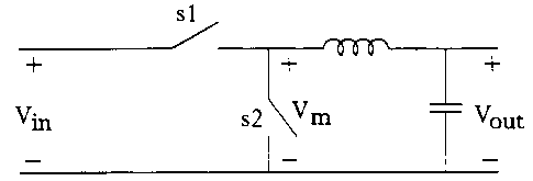
topology depicted in Figure 1, wherein bidirectional
switches sl and s2 are switched in a complementary fashion
such that the voltage across s2, denoted vnõ is equal to
either the input voltage, vin, or 0. If the ratio of the
time sl is "on" (i.e., closed) to the total switching period
is denoted k, then the effective value of vn, is kvin, which
is the primary mechanism by which the voltage transformation
:L5 is achieved. The L and C elements serve to filter out the
high frequency switching harmonics from v,,.
The approach depicted in Figure 1, however, _Ls
laden with difficulties. For example, the topology depends
on complementary switching of switches s1 and s2. If, for
:20 example, s2 is closed ever so slightly before sl is opened,
the source voltage viõ will be shorted, thus leading to a
current spike. If s2 is closed slightly after sl is opened,
then for that instant there will be no path for the current
in the filter inductor to flow, leading to a voltage spike.
25 Sirice physical devices do possess an impedance and are not
ideal switches, this approach is physically possible to
implement but is nevertheless problematic and subject to
high switching losses. Another disadvantage of this design
is that, at the voltage levels needed to implement a
30 distribution level transformer, semiconductors with
appropriately high voltage ratings are not available.
Series-connected devices must be used for this reason, but
such devices are problematic in that device voltage ratings
can be easily exceeded unless extreme care is taken to
35 insure voltage sharing during switching transients. A
CA 02333684 2000-12-01
WO 99/63650 PCTIUS99/12237
- 4 -
further disadvantage is that, when implemented as a single
stage, the semiconductors must be able to withstand both
full primary voltage and full secondary current - a very
expensive arrangement. Avoiding this difficulty requires
using multiple cascaded stages but this can be problematic
from a control perspective. In addition, the transformer
depicted in Figure 1 does not offer magnetic isolation. For
these reasons, solid state transformers based on the design
depicted in Figure 1 do not appear to be practical.
The following United States patents disclose
various aspects of a solid state transformer, but none
relates to a solid state distribution transformer capable of
handling voltage levels encountered by distribution
transformers: U.S. Patent No. 5,510,679, Apr. 23, 1996,
:L5 "Reverse Phase-controlled Dimmer with Integral Power
Adjustment Means"; U.S. Patent No. 5,270,910, Dec. 14, 1993,
"Neon Light Box"; U.S. Patent No. 5,038,081, Aug. 6, 1991,
"Reverse Phase-controlled Dimmer"; U.S. Patent No.
4,204,237, May 20, 1980, "Solid State Transformer
Differential Relay"; U.S. Patent No. 4,071,378, Jan. 31,
1978, "Process of Making a Deep Diode Solid State
Transformer"; and U.S. Patent No. 4,024,565, May 17, 1977,
"Deep Diode Solid State Transformer."
SDNMARY OF THE INVENTION
Accordingly, a primary object of the present
invention is to provide an improved solid state transformer
(SST) capable of use as a distribution transformer. A
presently preferred embodiment of a solid state distribution
transformer in accordance with the present invention
;10 comprises an input stage coupled to an isolation stage. The
input stage converts a high voltage, single phase AC input
voltage to a plurality of, or N, unisolated DC output
voltages, where each unisolated DC output voltage is at a
voltage level which is less than the voltage level of the
_15 peak SST AC input voltage. In addition, each of the
unisolated DC output voltages is separately isolated in the
CA 02333684 2000-12-01
WO 99/63650 PGT/US99/12237
- 5 -
isolation stage.
In a presently preferred embodiment of the
invention, the input stage comprises N input modules having
input ports, each comprising two input terminals, coupled in
series such that a first module and a last module are
coupled to receive the AC input voltage on one input
terminal and further coupled by another input terminal to an
input terminal of an adjacent input module. Each input
module other than the first and last modules is coupled by
two input terminals to two adjacent input modules.
Moreover, each input module further comprises an output
port, and the isolation stage comprises N isolation modules
each having an input port and an output port; and the output
port of each input module is coupled to an input port of a
corresponding isolation module. Further, the respective
output ports of the isolation modules are coupled together
in parallel to provide an isolated bipolar DC voltage
supply.
The preferred embodiment also includes an output
module coupled to the isolation stage. The output module
provides the desired AC output voltages (normally
approximately plus and minus 120 VAC) at the desired
frequency (normally 60 Hz or 50 Hz). In general, the SST
may be designed to accept a wide range of input voltages and
to provide a wide range of output voltages with any
combination of frequencies.
Preferably, each isolation stage module comprises
means for providing magnetic isolation between its input and
output voltages. The isolation provided by the isolation
modules permits the isolation stage modules, series
connected at their inputs, to be parallel connected at their
outputs, whereby voltage reduction is provided.
Other features and advantages of the present
invention will be apparent from the following detailed
:45 description of preferred embodiments.
CA 02333684 2000-12-01
WO 99/63650 PCT/US99/12237
- 6 -
BRIEF DESCRIPTION OF THE DRAWINGS
Figure 1 depicts the topology of an early solid
state transformer (SST).
Figure 2 schematically depicts an SST in
accordance with the present invention.
Figure 3 depicts an input stage module for an SST
in accordance with the present invention.
Figure 4 depicts an isolation stage module for an
SST in accordance with the present invention.
Figure 5 depicts an output stage module for an SST
in accordance with the present invention.
Figures 6 - 12 depict presently preferred
algorithms for controlling an SST in accordance with the
present invention. Figure 6 illustrates input stage
:L5 control; Figure 7 illustrates the input stage control
voltage regulator; Figure 8 illustrates the input stage
control voltage observer; Figure 9 shows the input stage
control current command synthesizer; Figure 10 depicts an
input stage control duty cycle synthesizer; Figure 11
depicts the isolation stage control; and Figure 12 depicts
the output stage leg control of the presently preferred
embodiment.
DETAILED DESCRIPTION OF PREFERRED EMBODIMENTS
A solid state transformer in accordance with the
present invention is schematically depicted in Figure 2.
The topology shown includes three stages - an input stage
10, an isolation stage 20, and an output stage 30. The
function of the input stage is to convert power from high
voltage, single phase AC to N DC ports, where N is the
number of input stage modules 12. Controllers 100, 200 and
300, explained in greater detail below with reference to
Figures 6-12, may be implemented as separate control
circuits or as a software controlled microprocessor or
digital signal processor (DSP), or the like.
A presently preferred topology for each input
stage module 12 is depicted in Figure 3. As shown, each
CA 02333684 2000-12-01
WO 99/63650 PCT/US99/12237
- 7 -
input stage module 12 includes a single phase full bridge
rectifier 14 coupled to what is essentially a boost
converter, comprising inductor 15, transistor 16, diode 17
and output capacitor 18. The transistor 16 is switched at a
predetermined frequency and the duty cycle is controlled so
as to cause the current in the inductor 15 to take the form
of a rectified sinewave, which causes the AC current into
the rectifier 14 to be sinusoidal. Note that the converter
used in each module is based on the topology shown in C. P.
Heinz and N. Mohan, A Digitally Controlled AC/DC Power
Conditioner that Draws Sinusoidal Input Current, IEEE PESC
Conference Record, 1986, pp. 531-540. However, the proposed
design is an extension of the prior design in the use of N
modules instead of a single module, which avoids the use of
:15 series connected devices in high voltage applications. In
addition, the switching of the individual transistors is
coordinated so that the effective switching frequency is N
times the actual switching frequency. This provides a
mechanism to provide very low distortion in the AC current
into the rectifier while maintaining a low actual switching
frequency, which in turn results in high efficiency through
minimization of the switching losses.
The output of each of the N input stage modules 12
is fed into the input of a corresponding isolation stage
module 22. The primary function of the isolation stage 20
is to provide magnetic isolation. In addition to providing
input/output isolation for the transformer (a desirable
characteristic), the isolation provided also permits the
isolation stage modules 22, which are series tied on the
input side as shown in Figure 2, to be parallel tied on the
output stage, which provides a convenient method for
achieving the bulk of the voltage reduction.
A presently preferred construction of an isolating
DC/DC converter is depicted in Figure 4. In this converter,
the DC input is converted to a high frequency AC square
wave, fed into a ferrite core-based transformer T (which is
small due to the high frequency) and then rectified in such
CA 02333684 2000-12-01
WO 99/63650 PCT/US99/12237
- 8 -
a way as to provide a bipolar DC output. Both the frequency
and duty cycle (the amount of time the voltage is non zero
over the period of the waveform) are varied so as to
optimize efficiency for a given load. Within this design it
is expected that the isolation transformers themselves could
advantageously be constructed using a single core in a
production unit. However, separate cores may be used in
order to facilitate construction with commercially available
parts.
The output stage 30 is depicted in Figure 5. The
function of the output stage is to convert from relatively
low voltage bipolar DC (a few hundred volts) to low voltage,
60 Hz AC, with a grounded secondary midtap. Switching is
based on a hysteresis current control algorithm, where the
current command is obtained from a feedforward type voltage
regulator. The algorithm automatically compensates for load
harmonics and has a built in current limit.
A more detailed discussion of the operation of the
solid state transformer (SST) will now be provided.
SST Control Algorithms
There are three main control algorithms for the
SST, one for the input stage 10, one for the isolation stage
20, and one for the output stage 30. These three control
algorithms act independently.
Figure 6 illustrates the input stage control. The
function of this control is to switch the input stage module
semiconductors so as to regulate the input stage DC output
voltages and at the same time to insure that the AC input
stage input current is sinusoidal and in phase with the
input voltage. As can be seen, this control consists of
four sub-algorithms - a voltage regulator 105, an input
voltage observer 110, a current command synthesizer 120, and
a duty cycle synthesizer 130.
The primary regulatory action of the control is
accomplished by the voltage regulator 105 illustrated in
Figure 7. Therein, the output voltage vo,,tl of the lowest
input stage module 12 is measured and then filtered. The
CA 02333684 2000-12-01
WO 99/63650 PCT/US99/12237
- 9 -
filtered quantity is then compared to a reference voltage
vref, and the error is an input to a proportional plus
integral (PI) type control. The output of the PI block is
then current limited, and the output of the current limit is
the desired zero-to-peak amplitude of the input current. In
the case that the current limit is reached, an anti-windup
routine is used to prevent wind up of the PI integrator.
The remainder of the input stage control sub-systems are to
achieve an input current with the desired waveshape
(sinusoidal) with the desired amplitude (1magJ-
The first of the controls used to achieve the
desired input current is the input voltage observer 110
(Figure 8). The function of input voltage observer is
threefold. First, it determines an idealized half rectified
voltage vr which corresponds to the instantaneous value of
the fundamental component of the input voltage (vsõ) after it
has been passed through an idealized rectifier. In
addition, it also determines the time derivative of this
quantity, denoted pvr, as well as the peak value of vr over a
cycle, denoted vrpk. A block diagram of this control is
depicted in Figure 8. Therein, the low pass filter LPF 1
comprises a series of three first order low pass filters
which have a time constant and gain such that, at a
frequency of 60 Hz, the collective output of the filters has
a gain of unity and a phase shift of 180 degrees. LPF 1
also utilizes a negative unity gain block so that the output
of this block (vin) is actually in phase with the input
voltage, though with most of the harmonic content removed.
A fourth first order filter with a fast time constant
:30 (t)is used to estimate the derivative of the filtered input
voltage (denoted pvin). The time constant of this filter is
such that negligible phase shift occurs at 60 Hz. Next, an
"analytical rectifier" is used to determine the output of an
idealized rectification of the filtered input voltage. This
:35 is used to determine the idealized rectifier voltage v,. as
CA 02333684 2000-12-01
WO 99/63650 PCT/US99/12237
- 10 -
well as the idealized time derivative of the rectified
voltage pvr. The idealized rectifier voltage vr is also fed
through another low pass filter (LPF 2) in order to
determine its average value, which is then multiplied by n/2
in order to determine the peak value of vr over a cycle.
Based on the outputs of the input voltage observer
110 and the voltage regulator 105, the current command
synthesizer 120 determines the instantaneous current
command, i' as well as the time derivative of that command,
pi' as shown in Figure 9. These quantities are determined
such that the peak value of i" is equal to the desired
magnitude 1õ,ay and that i" which is the commanded input stage
module inductor current, is a rectified sinusoid. If the
actual input stage module inductor current is equal to this
3.5 value, it follows that the input current will be a sinusoid
with a peak value of lmaq =
The last aspect of the input stage control is the
duty cycle synthesizer 130 shown in Figure 10. The function
of this control is to determine the duty cycle (diõ) of the
input stage modules such that the input stage module
inductor current, 1-lbstl, is equal to the current command i" .
As can be seen, this is based on the idealized rectifier
voltage vr, the instantaneous current command i* as well as
its time derivative pi', the input stage inductor current
i1bstl, and the DC output. voltage of the first input stage
module vout1. Based on the commanded duty cycle, the amount
of time each transistor is on in each module per switching
cycle may be readily calculated. It should be noted that
the switching of each module is staggered so that the
effective switching frequency is equal to the number of
modules times the base switching frequency.
Figure 11 depicts the isolation stage control 200.
The principal variables in this control are the isolation
stage output voltage vd,:out, the commanded output voltage
CA 02333684 2000-12-01
WO 99/63650 PCT/US99/12237
- 11 -
v"d,,o.t, the isolation stage master input module DC input
voltage, vdcin (which is equal to the input module output
voltage voõtl), the secondary rectifier output current
command, i'r, the secondary rectifier output current limit,
irlim, the duty cycle dis and the switching period Ti9.
Parameters include the lag filter time constant, Tlf, the lag
filter gain Kp, the number of isolation stage transformer
secondary turns, ns, the number of isolation stage
transformer primary turns, np, the effective transformer
:LO leakage inductance seen from the secondary side Leff, and the
H-bridge transistor peak current limit lpklim =
In the isolation stage 120 (Fig. 2), the converter
semiconductors are switched such that the primary side
voltage on the isolation voltage takes on a value of vd,i,õ 0,
:L5 -Vdin, 0 and then repeats. The period of this repetition is
denoted Tig. The duty cycle (di.) is defined as the amount of
time the primary voltage is nonzero divided by the switching
period Tis. The function of the isolation stage is to
control the duty cycle dis and period T19 such that the
20 isolation stage output voltage vdo,,t is equal to its
commanded value v"d,o,t in such a way as to achieve maximum
isolation stage efficiency.
The operation of the isolation stage control, is
as follows. First the output voltage command Wdcoõt) is
25 compared with the actual voltage (vd,oõt) and the error is fed
through a first order lag transfer function, whose output is
a current command, which is limited to the variable current
limit, irllm (this is an average current limit which is
calculated such that a peak current limit is approximately
30 achieved). Based on the limited current command, a duty
cycle command that (dis) will approximately achieve that
current is computed and bounded to values between 0 and 1.
The duty cycle is directly used to compute the relative
amount of time the transistors in the H-bridge 236 (Fig. 4)
CA 02333684 2000-12-01
WO 99/63650 PCT/US99/12237
- 12 -
of the isolation stage should be on. In addition, the
duty-cycle is fed through a low pass filter (LPF), and the
result is an input to a look up table, whose input is the
filtered duty cycled and whose output is the switching
period Ti9. This look up table is created such that maximum
efficiency is obtained for a given operating condition..
Given that switching period T19 and the duty cycle dis, the
switching of the H-bridge semiconductors is readily
determined. In addition, based on the switching period Ti,s,
3.0 the current limit lrlim is calculated.
The output stage control 300 comprises two
independent but identical controls that each control one
phase leg of the output stage 30 (Fig. 5). The output stage
leg control is depicted in Figure 11. Therein, v', (where x
1.5 is "a" for the a-phase leg and "b" for the b-phase leg) is
the commanded output voltage of one line-to-midtap voltage,
which is commanded to be a sinusoid of the desired
frequency. This is compared to the corresponding line-to-
midtap voltage, and the error is multiplied by a constant of
20 proportionality and then added to the measured output
current i, and then limited to ilim. The resulting value is
the leg current command i",, which is achieved using a
hysteresis current regulator.
Gate Drive Control of Transistors
25 Gate drive circuits of the type that may be
employed in practicing the present invention are well known,
and need not be described in detail herein. However, the
following remarks should be considered in designing a
specific embodiment of the present invention.
30 Although the gate drive circuits are standard, the
preferred embodiment of the inventive SST has some special
features in regard to the power supply and signal transfer
from the controls to th.e gate drive circuits. Power for the
gate drive circuits is derived from the SST output. In
35 particular, a low-power 60-Hz transformer, similar to the
one found on PCS, etc., is connected to the SST output. The
CA 02333684 2000-12-01
WO 99/63650 PCTIUS99/12237
- 13 -
60-Hz low-voltage step down transformer output is then
rectified to provide a low-voltage DC source. This source
is used to feed an inverter whose output is connected to a
low-power high-frequency transformer to provide a low-
voltage, high-frequency (20-40 kHz) AC source. The low-
voltage, high-frequency AC is used as an internal-power
source for all the sensing, control, and gate drive
electronics. Each of these devices interfaces to the low-
voltage high-frequency distribution system through a small
:L0 low-power transformer. Startup power is provided by a
battery on the low voltage DC link.
Because of the large potentials existing between
various modules in the SST, one problem that arises is that
the internal-power transformers (which are very small
3_5 because they are very low power and operate at very high
frequencies) would normally have to provide over 10 kV of
isolation. The spacing requirements to achieve this would
normally make the interface transformers undesirably large.
To alleviate this problem, a cascade of transformers is used
20 to supply power to the input and isolation stage modules
(the output stage has its own gate drive and control
internal-power transformer connection since it is at a low
potential relative to the internal power supply). In this
arrangement, the first transformer of the cascade connects
25 to the internal power supply. It has multiple secondary
windings to provide magnetically isolated internal power to
all gate drives and sensors associated with the first
isolation and input stage modules. It has another secondary
winding connected to the primary winding of the second
30 internal-power distribution transformer in the cascade,
which in turn has secondary windings that provide isolated
power to all internal loads on the second input and
isolation stage modules and a secondary winding to provide
power to the transformer of the third module. This
35 arrangement continues until all modules are provided for.
An advantage of this arrangement is that the isolation level
builds as the voltage level goes up, and so each internal
CA 02333684 2000-12-01
WO 99/63650 PCTIUS99/12237
- 14 -
power distribution transformer need only to be able to
provide isolation between stages, not from the highest
potential stage to the lowest potential stage.
The use of cascaded isolation is also used in
regard to the control signals with the isolation and input
stages. Normally, isolation between the controls and the
power stage could be achieved using opto-isolator integrated
circuits (ICs). Unfortunately, these devices are not
available with ratings sufficient for the SST. Fiber optics
offer almost infinite isolation but they are expensive. As
a solution to this problem, the preferred embodiment of the
SST makes use of a cascaded control signal system wherein
the first module (both input and isolation) can communicate
with the controls using opto-isolators (since they are at
similar potentials). The first module communicates with the
second, the second with the third, and so on, with each
connection making use of an additional opto-isolator
providing the additional voltage isolation needed to go one
level higher. Opto-isolator ICs are adequate for this
application because the isolation being provided is only
that between stages. Because of the structure of the
controls, only four signals need to be passed through the
input and isolation stage modules in this way. These
signals include the input stage duty cycle, an input stage
:25 synchronization signal (used to insure that each module
switches at the correct time to achieve the desired
multiplication in the effective switching frequency), and
two signals describing the switching state of the isolation
stage switching devices.
In sum, the solid state distribution transformer
disclosed herein provides transformation between voltage
levels through the use of power electronic converters rather
than through the use of magnetics, although a high frequency
isolation transformer is also used. When compared to
3 5 conventional distribution transformers, the advantages of an
SST in accordance with the present invention include: (i) no
mineral oil is needed; (ii) it is expected to weigh less;
CA 02333684 2000-12-01
WO 99/63650 PCT/US99/12237
- 15 -
(iii) it is expected to be smaller; (iv) it mitigates all
power quality issues at the load (i.e., it can compensate
for non-sinusoidal loads, DC offset loads, input voltage
variation, input voltage distortion); and (v) it provides
unity power factor at the transformer's input regardless of
the power factor at the transformer's output. In addition,
the input and output frequencies do not have to be the same,
which could be advantageous, e.g., on a U.S. military base
residential area in European countries. Further, the output
stage could be changed to provide three-phase power. The
SST also features a DC' bus capable of supporting motor
drives and may also be readily interfaced to energy storage
devices (such as batteries) for operation as an
uninterruptable power supply.
The scope of protection of the following claims is
not intended to be limited to the presently preferred
embodiments disclosed above. There are, e.g., possible
variations in the preferred embodiments that may be
implemented without departing from the true spirit of the
invention. For example, the isolation stage 20 may be
replaced by any type of isolating DC/DC converter. In
addition, the inventor anticipates that the isolation
transformers T of all of the isolation stage modules 22
could actually be combined into a single high frequency
.25 transformer with multiple secondaries and a single center
tapped primary. Additional possible design modifications
include using soft switching converters in the isolation
stage 20, and the use of either soft switching or multi-
level converters in the output stage.
:30 Moreover, embodiments of the invention could be
designed for almost any input voltage by adding additional
input stage modules. In regard to output voltage, the only
limitation is the voltage rating of the output stage
semiconductors. With today's commonly available 1200 V
:35 devices, up to +/-400 V would be easy to achieve. With
somewhat less available 1800 V devices, +/-600 V should be
achievable with little modification. If one takes advantage
CA 02333684 2000-12-01
WO 99/63650 PCT/US99/12237
- 16 -
of a multi-level design, the output voltage could be further
increased. In regard to frequency, the maximum switching
frequency somewhat drives this concern. With presently
available semiconductor technology, up to about 400 Hz is
achievable. These numbers will change with time as new and
better semiconductors become available.