Note : Les descriptions sont présentées dans la langue officielle dans laquelle elles ont été soumises.
CA 02334975 2000-12-06
WO 99167$77 PCTIGB99101932
Synthesising a Sine Nave
The ~ present invention relates to a method and apparatus for synthesising
approximations to sine waves over a range of frequencies.
As shown in Figure 6, an approximation to a sine wave S may be generated from
a
conveniently compact device by combining a number of pulse width modulated
signals 102,103,104 generated by a microprocessor from its own clock signal
101. In
order to produce a sine wave 105 having a different frequency, the frequency
of the
clock signal 101 is divided by a number such as 1,2,3,4...etc. However, this
produces
discrete coarse steps in the resultant range of sine wave frequencies
produced. For
example if the clock signal in Figure 6 has a frequency of 16 MHz, as may be
used
with a microprocessor, the highest sine wave frequency that can be synthesised
in this
example is IMHz, as sixteen clock cycles are needed to synthesise each sine
wave
cycle. The next highest sine wave frequency available is achieved by halving
the
clock frequency to 8 N(Hz producing a sine wave of 500 kHz. The next highest
sine
wave frequency is aclueved by dividing the clock frequency by three to give a
frequency of 5.3 MHz producing a resultant sine wave frequency of 330 kHz and
so
on.
As can be seen, large discrete steps or poor frequency resolution is produced
in the
resultant range of sine 'wave frequencies available.
According to a first aspect of the present invention an apparatus for
synthesising an
approximation to a sine wave comprises:
CA 02334975 2000-12-06
W~ 99/6'1877 PCT/GB99l01932
means for generating a number of pulse width.modulated signals from a clock
signal; and
means for combining the generated pulse width modulated signals to produce
an approximation to a sine wave;
wherein the clock signal is provided by an oscillator arranged to produce
clock signals over a continuous range of frequencies.
According to a further aspect of the present invention a method of
synthesising an
approximation to a sine wave comprises:
generating a number of pulse width modulated signals from a clock signal;
and
combining the generated pulse width modulated signals to produce an
approximation to a sine wave;
wherein the clock signal is provided by an oscillator arranged to produce
clock signals over a continuous range of frequencies.
The use of the oscillator to produce clock signals over a continuous range of
frequencies enables the production of resultant sine waves with a continuous
range of
frequencies rather than the discrete range discussed above.
The oscillator preferably produces a variation in its output clock signal
frequency as a
result of a variation in an input controlling electrical signal. The input
controlling
z
CA 02334975 2000-12-06
WO 99167877 PCTIGB99101932
electrical signal that is varied is preferably a voltage.making the oscillator
a voltage
controlled oscillator.
The output frequency of the oscillator and also of the approximation to a sine
wave
can thus be controlled by simply varying an input signal to the oscillator.
The approximation to a. sine wave may be "smoothed" to remove at least some of
the
high frequency components by passing the signal through a low pass filter.
The sine wave produced may be used in a number of applications such as to
match
the frequency of the produced sine wave with the frequency of another detected
signal or to provide stimulation which produces a particular effect at a
particular
unknown frequency mhich is then detected. In such applications it would be
desirable to be able to determine the particular frequency which, in the above
examples matches the detected frequency or produces the particular effect. The
frequency need not necessarily be consistently related to the controlling
input signal
applied to the oscillator but may be variable due to, for example temperature
changes.
To accurately determine a particular frequency of a synthesised approximation
to a
sine wave, the number of cycles of one of the pulse width modulated signals or
the
clock signal produced over a given period of time such as one second may be
counted
and/or the time taken to produce a fixed number of cycles may be measured and
from
this the frequency dete~~mined.
3
CA 02334975 2000-12-06
WO 99/67$77 PCT/GB99/01932
The -means for generating pulse width modulated signals from a clock signal is
preferably a processing means.
The invention is des<;ribed further by way of example with reference to the
accompanying drawings in which:
Figure 1 is a block dia;;ram illustrating the overall operation of a system to
measure
the speed of sound of a gas using a resonator;
Figure 2 shows a substtmtially spherical resonator that can be used in the
system;
Figure 3 shows how thE; acoustic receiver is mounted to the resonator;
Figure 4 shows how the; acoustic transmitter is mounted to the resonator;
Figure 5 shows the amplitude of a signal detected by the acoustic receiver
over a
range of frequencies;
Figure 6 illustrates how a clock signal is used to produce pulse width
modulated
signals which are combined to produce an approximation to a sine wave;
Figure 7 shows an electronic system to perform the operation illustrated in
Figure 6;
4
CA 02334975 2000-12-06
WO 99/67877 PCT/GB99/01932
Figure 8 shows a voltage controlled oscillator to supply the clock signal to
the system
shown in Figure 6;
Figure 9 shows a sequence of aperations to determine the resonant frequency;
Figure 10 shows the connections to a processing means to determine resonant
frequency; and
Figure 11 shows a method of allowing for the finite hardware response time.
As shown by Figure 1., driving electronic circuit 1 which may include or be in
the
form of a microprocessor is arranged to produce a sinusoidal signal aver a
suitable
range of frequencies to drive a loudspeaker 2. The loudspeaker is arranged to
apply
an acoustic signal to the interior of a resonator 3. Microphone 4 is arranged
to pick
up the magnitude of the acoustic signal within the resonator. The signal from
the
microphone is filtered and amplified by an appropriate electronic circuit 5
and a
processing means 6 de~;ermines the resonant frequency relating to the gas
within the
resonator to determine iits speed of sound.
The resonator 3 shown in Figure 2 is in this case a rigid sphere. The
illustrated
resonator is formed from two CNC (computer numerically controlled) machined
CA 02334975 2000-12-06
WO 99167877 PCT/GB99I01932
metal hemispheres 31,32, in this case made of copper, of internal radius l.5cm
and
3mrn wall thickness welded together to form the sphere.
The apexes of hemispheres 31,32 support the loudspeaker 2 and microphone 4
respectively which when the hemispheres are joined as shown in figure 2 are
substantially 180° apart to provide the largest amplitude microphone
signal.
The resonator is provided with a number of gas diffusion passages 33, only one
of
which is shown in Figure 2, to enable gas to diffuse in and out of the
resonator 3.
Each hemisphere 3I, 32 is preferably provided with four gas diffusion passages
33
positioned 90° apart. Gas diffusion passages 33 are preferably drilled
through the
resonator housing and any swarf removed to present a regular repeatable
surface to
the inside of the resonator.
Alternatively the resonating sphere could be made from a porous material such
as a
sintered material. Gas diffusion holes 33 shown in the copper resonating
sphere of
figure 2 would then not: be required and so would reduce perturbations in the
resonant
frequency due to the holes 33. The porous material used would preferably have
a
lower thermal expansion than copper, reducing the amount of correction
required for
variation in the size of the resonator with ambient temperature changes.
6
CA 02334975 2000-12-06
WO 99167877 PCT/GB99101932
The loudspeaker 2 is in this case a miniature loudspeaker as may be used in a
hearing
aid with a supply voltage of 5V and a power level of approximately 33mW and
the
microphone 4 is a sub-miniature microphone.
Figure 3 shows how the microphone 4 is mounted to the resonator 3. The
resonator is
provided with a passal;e 41 of approximately l.5rnm diameter which is
preferably
drilled and any swarf removed. A cylindrical spindle 42 is mounted to or
formed as
part of the outside of tl'ne resonator and arranged concentrically with the
passage 41.
The spindle 42 is preferably approximately l Omm in length and has an inner
diameter
sufficient to accommodate the microphone 4, in this case approximately 5mm.
The
position of the microphone 4 within the spindle is variable along its length
so that it
may be positioned at the optimum point at which the sharpest output signal
peak is
produced, when the loudspeaker applies the resonant frequency to the
resonator. The
microphone 4 is secured at the optimum position within the spindle 42 using
adhesive
43. The adhesive is preferably prevented from entering the resonator cavity as
it
could dry in irregular shapes which may cause perturbations in the resonant
frequency. The microphone 4 is preferably provided with a rim 45, the outside
diameter of which is substantially the same as the inside diameter of the
spindle 42 to
prevent any adhesive entering the resonator. Alternatively the microphone 4
could fit
tightly in the spindle 42. The microphone 4 is connected to the driving
electronics 1
by an electrical connection 46.
CA 02334975 2000-12-06
WO 99/67877 PCT/GB99/01932
The loudspeaker 2 may be mounted in the same manner as the microphone 4 shown
in Figure 3, but is in this example $xed at a particular distance from the
inside of the
resonator as shown in Figure 4.
In Figure 4 a spindle 21 of approximately 2mm length is mounted to or formed
as
part of the outside wall of the resonator 3 and a 1.Smrn passage 22 drilled
through the
spindle 21 and the resonator wall with any swarf removed. The loudspeaker 2 is
mounted to the outside of the spindle 21 covering the passage 22. The
loudspeaker is
secured to the spindle 21 using adhesive, ensuring that no adhesive enters
passage 22
and is electrically connected to filtering and amplifying electronics S by
electrical
connection 23.
The position of both the microphone and loudspeaker may be variable to attain
the
sharpest output peak on alternatively either the microphone or loudspeaker may
be
fixed with the position of the other being variable.
Because of slight variations in each resonating sphere due to machining
tolerances for
example producing difi:erent effective radii, each resonator is calibrated
individually
using the expression:
c=fxl<;
8
CA 02334975 2000-12-06
WO 99/67877 PCT/GB99/01932
Each resonator is calibrated using a gas of known speed of sound (c) found
using a
computer model for predicting gas characteristics such as GASVLE or by
measurement using some suitable method. The resonant frequency (f) is then
measured for the gas of known speed of sound in the resonator being calibrated
and
the constant K found. Using the calibrated resonator together with its
associated
constant K allows the speed of sound to be determined for any gas from the
measured resonant frequency. This gives accuracies of about 0.1 %. By
compensating
for variations in ambient temperature affecting the volume of the resonator,
the speed
of sound of a gas may be determined to even better accuracies of about 0.05%.
The loudspeaker is driiven by an electronic circuit 1 shown diagrammatically
in
Figure 1 to provide sinusoidal signals over a frequency range suitable to
encompass
the frequency of the first non-radial resonance peak of the resonator 3. The
loudspeaker is driven in frequency sweeps. The microphone provides an output
voltage, which is filtered and amplified, corresponding to the frequency at
which the
loudspeaker is currently being driven as shown graphically in Figure 5 with a
small
delay due to electronics. The frequency at which the microphone produces the
largest
output voltage is determined to be the non-radial resonant frequency which in
Figure
is 8860 Hz at 20°C.
The generation of approximations to sine waves over a continuous range of
frequencies is described below.
9
CA 02334975 2000-12-06
WO 99/67877 PCT/GB99J01932
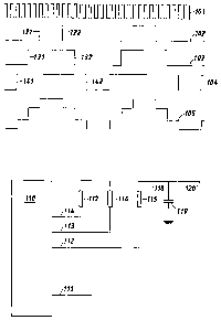
As shown in Figures 6 and 7, a clock signal 101 is applied to a microprocessor
110 on
line 111 from a voltage; controlled oscillator. Any suitable microprocessor
may be
used such as a Hitachi HD6473048F16. The microprocessor 110 processes the
input
clock signal 101 from line 111 to produce pulse width modulated (PWM) signals
102,103 and 104 shown in Figure 6, each of the same frequency on lines 112,113
and
114 respectively. The 1'WM signals 102, 103, 104 are combined together using a
weighted summing arrangement, in this case consisting of resistors 115,116,117
to
produce the approximation to a sine wave on line 118. The approximation to a
sine
wave 105 shown in Figure 6 has the same frequency as the PWIVI signals
102,103,104 which each have fixed duty cycles (percentage time on to
percentage
time offj.
In this example each cycle of the synthesised approximation to a sine wave 105
corresponds to sixteen cycles of the clock signal 101, but could be eight or
thirty two
or any other suitable amount. The rising 121 and falling 122 edges of PWM
signal
102 are triggered by the completion of the sixth and tenth cycles of the clock
signal
101 respectively. The rising 131 and falling 132 edges of PWM signal 103 are
triggered by the complc;tion of the fourth and twelfth cycles of the clock
signal 10I
respectively. The rising 141 and falling 142 edges of PWM signal 104 are
triggered
by the completion of the second and fourteenth cycles of the clock signal 101
respectively.
CA 02334975 2000-12-06
W4 99/67877 PCT/GB99l01932
Each of PWM signals 102,103 and 104 is then passed through a weighting
resistor
115,116,117 respectively. The ratio of the values of resistors 115,116,117 is
chosen
to give the best overall sine wave approximation which in this case is
resistor 115
being 51 kS2, resistor 116 being 36 KS2 and resistor 117 being 51 kS2.
To produce an approximation to a sine wave from PWM square waves it is
desirable
to maintain the first harmonic whilst suppressing the third, fifth, seventh
etc
harmonics. Using the above method as illustrated in Figure 6 the third and
fifth
harmonics are essentially removed apart from some residual effects due to
resistor
tolerances. In the present example it is envisaged that the sine wave
generating
apparatus will be used to generate sine waves in the range of 7.5kflz-11.8kHz
to
drive the loudspeaker ?. and the transmitted signal from the loudspeaker
detected by
the microphone 4. When used in this manner the seventh and subsequent
harmonics
are reduced to levels such that no further filtering or conditioning should be
needed to
remove the effect of these harmonics since the transmitted signal due to these
harmonics should lie outside the band-pass limits of the microphone. If the
apparatus
is used to generate sine waves at lower frequencies, the effect of the seventh
and
subsequent harmonics could be removed or diminished by low pass filtering or
using
more pulse width modulated signals to produce a better approximation to a sine
wave.
The output from each resistor 115,116,117 is combined at common line 118 to
produce the approximation to a sine wave 105 shown in Figure 6. The signal 105
is
11
CA 02334975 2000-12-06
WO 99/67877 PCTlGB99/01932
low pass filtered by capacitor 119 connected between common line 118 and earth
and
is detected at connection point 120.
Figure 8 shows a valt;age controlled oscillator 160 which produces an
oscillating
output at 161, the frequency of which is dependent upon the voltage of a
driving
signal applied at input 1b2. However any device the output frequency of which
is
dependent upon the analogue value of an input is suitable.
The present example of the invention uses an Analog Devices AD654 voltage to
frequency converter. ~Che AD654's black diagram appears in Figure 8. A
versatile
operational amplifier 163 serves as the input stage; its purpose is to convert
and scale
the input voltage signal 162 to a drive current. A drive current is delivered
to current
to frequency converter 165 {an astable multivibrator). The output of converter
165
controls transistor 164.
In the connection scheme of Figure 8, the input amplifier 163 presents a very
high
(250 MS2) impedance to the input voltage at 162, which is converted into the
appropriate drive current by the scaling resistor 167 at Pin 3. In this
example resistors
167 and 168 are 1.2 kS.~.
The frequency of the approximation to a sine wave produced at the output
connection
point 120 shown in Figure 7 cannot always be accurately assumed from the
voltage of
the driving signal applied at input 162 shown in Figure 8 due to variations in
12
CA 02334975 2000-12-06
WO 99/67877 PCTJGB99101932
temperature and the performance of electrical components for example.
Consequently the microprocessor 110 may also be connected to any of lines
112,113
or 114 carrying PWM signals i 02,103 and 104 respectively which are at the
same
frequency as the output approximation to a sine wave as described later. The
microprocessor counts 'the number of cycles of the selected PWM signal over a
given
period of time such as one second. The actual output frequency of the sine
wave can
then be accurately determined. The microprocessor 110 counts the number of
cycles
of a PWM signal 102,1.03,104 rather than the cycles of the approximation to a
sine
wave 105 over a given period of time as the PWM signals have more precisely
defined, clear on/off states which are easier to count providing better
results.
Alternatively the microprocessor 110 could count the number of cycles of the
clock
signal 101 over a given period of time and from this determine the sine wave
frequency by dividing by the number of clock signal cycles required to produce
each
PWM signal cycle.
Alternatively or additionally the microprocessor may measure the time taken to
produce a predetermined number of clock cycles or P~~VM cycles and from this
calculate the frequency of the approximation to a sine wave.
As the oscillator 160 produces an oscillating signal with a continuous range
of
frequencies, sine wave.. may be generated with a continuous range of
frequencies.
13
CA 02334975 2000-12-06
WO 99167877 PCT/GB99/01932
Use of a variable frequency square wave generating oscillator which is a
readily
available, small, (9.9I;mm x 7.87mrn x 4.S7mm in 8-pin plastic DIP form or
4.90mm
x 3.9Imm x 2.39mm in 8-Pin SOIL form for the AD 654), cheap device in
conjunction with a microprocessor to produce approximations to a sine wave
enables
the production of a dcwice which is able to generate approximations to sine
waves
over a continuous range of frequencies and which is compact and so may be
mounted
on a compact probe for example or in a compact housing. Since a microprocessor
is
generally employed in many probes or electronic systems for other purposes,
the only
additional space that is required to produce approximations to sine waves over
a
continuous range of frequencies is that for the compact variable frequency
square
wave generating oscillator.
The oscillator need not be a voltage controlled oscillator but may be any
device
arranged to supply a signal with a continuous range of frequencies
The approximation to a sine wave need not be generated from three PWM signals
but
could be generated from any suitable number depending upon the required level
of
the approximation to a sine wave. Furthermore each cycle of the sine wave need
not
correspond to sixteen clock cycles but could be eight, thirty two or any
suitable
number.
To quickly and accurately determine the resonant frequency (the frequency at
which
the amplitude of the signal produced by the microphone is a maximum) an
initial fast,
14
CA 02334975 2000-12-06
WO 99/67877 PCT/GB99101932
coarse frequency sweE;p is made (in this case IO-15 Hz steps) over the
frequency
range in which the resonance may occur as shown by S I in Figure 9. A control
means such as a microprocessor identifies a narrower frequency range within
the
initial coarse frequency sweep in which a maximum occurs. A further frequency
sweep S2 is made with smaller frequency steps (in this case 1Hz) within this
identified narrower frequency range to accurately determine the frequency at
which
the maximum occurs, identifying the frequency of resonance.
Using the above combination of coarse then fine frequency sweeps over a
narrower
frequency range, an accurate value of the resonant frequency may be quickly
determined for example in a fraction of a second. A control means such as a
microprocessor may average subsequent detected frequency values S3 to reduce
errors due to noise. The frequency of the PS~M signal may then be determined
S4 to
indicate the frequency of the generated sine wave driving the loudspeaker 2 at
resonance.
The determination of the resonant frequency will now be explained in detail.
A microprocessor, wlach in this case is the microprocessor IIO described
earlier
which also generates the PWM signals, is used to perform an algorithm to
determine
the resonant frequency of the gas within the resonator. Instead of the
microprocessor
110 a PC cQUld be used with an appropriate plug-in data acquisition card.
CA 02334975 2000-12-06
WO 99167877 PCT/GB99101932
To determine the resonant frequency, as shown in Figure 10, the microprocessor
110
has an analogue output :?01, a digital input 202 and an analogue input 203.
The analogue output 201 is connected to input 162 of voltage to frequency
convertor
160 shown in Figure 8, to control the frequency applied to loudspeaker 2. In
this case
the analogue output 201 consists of two outputs {not shown), both of which are
connected to input 162 of voltage to frequency converter 160. One ouptut
controls
the coarse frequency sweep and the other controls the fine frequency sweep.
Each of
the two outputs is passed through a digital to analogue converter, which in
this case is
provided in the microprocessor 110 itself, and an appropriate resistor to
provide the
required level of resolution. In this case the resistor for the coarse
frequency control
is 36kS2 and the resistor for the fine frequency control is 2.2MS2.
As explained earlier, the frequency of the approximation to a sine wave signal
which
drives the loudspeaker cannot always be accurately assumed from the voltage of
the
driving signal from analogue output 201 due to temperature variations and the
performance of electrical components for example. Thus one of the PWM signals
102,103,104 which are each at the same frequency as the approximation to a
sine
wave driving the loudspeaker 2 or the clock signal 101, is applied at digital
input 202
for the microprocessor 110 to calculate the frequency of the approximation to
a sine
wave 105 as described f;arlier.
16
CA 02334975 2000-12-06
WO 99167877 PCT/GB99/01932
The analogue input 203 represents the amplitude of the signal being received
by the
microphone and is connected to microprocessor 110 via an external analogue to
digital converter. The process of locating the resonant frequency is one of
identifying
the frequency at which the analogue input 203 is a maximum.
The process of locating the resonant frequency can be broken down into four
stages.
The first three stages S1, S2, S3 each involve changing the loudspeaker
frequency to
search for the resonance. When the resonance has been located, the final stage
S4
measures the resonant frequency.
The first stage S 1 is a fast scan through the permissible range of
frequencies taking
about one reading of the analogue input 203 for each step of the analogue
output
voltage 201. The permissible range of frequencies is selected to restrict the
scan to
those frequencies at wluch the non-radial resonance should occur for the
expected
combination of gas composition, temperature and pressure. The limits of the
permissible range are imposed to reduce the time taken to locate the resonant
frequency and also to reduce the risk of locating an unwanted resonant peak.
Although the exact relationship between the control voltage from the analogue
output
201 and the microphone frequency is not known, it can be approximated
sufficiently
well to be used to set the frequency limits of the permissible range within
which to
search for the resonance. In the present example the frequency range is 7.SkHz
to
11.8Khz (4.3 kI-~z} with a frequency scan rate of $6 kHz/second and a
microphone
17
CA 02334975 2000-12-06
WO 99/67877 PCT/GB99/01932
sampling rate of 100,000 sampleslsecond producing a total of 5100 microphone
samples in each direction.
To locate the resonance frequency the processor is arranged to look for a peak
in the
amplitude of a signal fram the microphone at input 203 and then ascertain the
frequency control voltage that was being used at the time.
To allow for the finite time the hardware takes to produce a change in the
amplitude
of the signal from the microphone at input 203 as a result of a change in the
frequency control voltage at output 201, the fast scan of the first stage S1
involves a
first scan up through the range of analogue output voltages 201 and a second
scan
down through the same range of analogue output voltages. Clearly the first
scan
could alternatively be down through the range of analogue output voltages and
the
second scan could be up through the range. When scanning up, the frequency
control
voltage 201 being applied when the peak is detected will be, due to the
response time,
slightly higher than the; voltage that caused the peak to occur. When scanning
down,
the frequency control voltage 201 will be slightly lower than the peak
voltage.
Assuming that the response time is the same for both scan directions, the
average of
the two voltages will give the true voltage at the resonance.
A second method of allowing for the finite response time of the hardware is
shown in
Fig.l l in conjunction with the above method of first and second scans in
opposite
directions. The second method uses an estimated value for the response time T
to
~s
CA 02334975 2000-12-06
WO 99/67$77 PCT/GB99/Oi932
match the peak 30i of the received microphone data values M to the frequency
control voltage V which, according to the estimated response time T and the
characteristic of the frequency control voltage with time 302, produced that
microphone data value as shown by the broken Iines 303 in Figure 11.
Consequently
the microphone continues to collect data for a time after the frequency
control voltage
V has finished scanning; at a time t,. This second method enables peaks that
lie near
to the end of the scan limits such as peak 301 in the upward scan of frequency
control
voltage 302 in Figure 11 to be found which if the collection of microphone
data M
had been synchronised to the scanning of the frequency control voltage 302
would
have been missed. If the estimated response time was accurate, the values X,Y
found
for the voltages producing the resonant peak in each of the up and down scans
would
be exactly the same. However, as shown in Figure 1 l, the estimated value may
be
slightly inaccurate in which case the up and down values of the frequency
control
voltage will be slightly different and will then be averaged.
The second stage S2 usf;s the scanning method of the first stage except over a
smaller
frequency range, identified in the first stage as containing the resonant
peak. The
second stage uses the value for the frequency control voltage at resonance
obtained
by the first stage as its centerpoint for its smaller frequency scan range. In
this
example the frequency ;>can range of the second stage is 150.SHz.
However the result of the first scan may be too close to one of the end limits
of the
frequency control voltage range for the second stage to be able to use it as a
19
CA 02334975 2000-12-06
WO 99/67877 PCTlGB99101932
centerpoint. In this case the scan of the second stage will be anchored at the
appropriate end limit of the frequency control voltage range.
The frequency control voltage step size is also different for the second
stage. For
speed, the first stage does not use the full frequency control voltage
resolution
whereas the second stage does to produce a more precise resonance frequency
value.
The second stage also uses a slower rate of change of loudspeaker frequency
with
time. In this case 2.15k;Hzlsecond rather than 86.OkHz/second used in the
first stage.
In this example the microphone sampling rate of the second stage is also lower
at
25,000 sampleslsecond producing a total of 1800 microphone samples.
The final value is obtained using the third stage S3 which uses a further scan
which
averages the microphone data and hence produces a dependable result. Like the
second stage, this sta ge uses the result obtained by the preceding scan as
its
centerpoint. If the result of the second scan is too close to an end limit of
the
frequency control voltage range for the third stage S3 to be able to use it as
a
centerpoint, the third scan could be anchored at an appropriate end limit of
its
frequency control voltage range. However, the scan of this third stage is
slower and
more methodical than tile scans of previous stages. Hence, it covers a range
of fewer
frequency control voltage values, generally 24 or less, and in this case 21.
For each
value the analogue output 201 is set and then the circuit is left to settle
for a few
milliseconds, in this case 5 milliseconds. When the settling time has elapsed,
a given
CA 02334975 2000-12-06
WO 99/67877 PCT/GB99/01932
number of samples of the microphone voltage are taken, in this case 20, and
summed.
This process is repeated for each frequency control voltage value and the peak
value
ascertained. This is the resonant frequency control voltage value.
The f nal fourth stage f~4 comprises holding the frequency at the resonant
value and
measuring the frequency of the signal driving the loudspeaker 2 using a PWM
signal
102,103,104 or clock si;~al 101 supplied to the digital input 202.
21