Note : Les descriptions sont présentées dans la langue officielle dans laquelle elles ont été soumises.
RCV.1'ON:EPA MUIr.'~CHFN U1 :14- 9- U : 18::3Ei : OlAEiS 841371-~ 't'ly 8'J
'~~;'J'~'t4f'S'~ 4
1'f-'Cr-GrJrIYJ 11:JJ ~1CLJI'l:~lcT fW-111"1 6 xGIYI.C YJlOOJ-O'f1J11 IV:'r"y7
D7 C.J7T~"10:~ r.IfJYJ~1'CJ~JO
PCT/GB99/02012
14-09-2000
i
1 i
INTEGRATED OPTICAL DEVICE PROVIDING ATTENUATION
TECHNICAL FIELD
This invention relates to integrated optical devices such as integrated
silicon waveguides for use in optical circuits.
BACKGROUND ART
integrated optical devices can include silicon waveguides formed on
the upper surface of a silicon wafer. Figure 1 shows such a construotion.
in which a rib waveguide 10 is formed on a layer of silicon 12. The silicon
layer 12 is silicon-on-insulator, having been grown epitaxially over a silica
layer 14 within a silicon wafer 18. The entire waveguide is coated for
protective purposes with the silica layer, 18. As a result, light propagates
within the waveguide 10,
The actual distribution of optical energy is in fact within the ions 20.
This extends within the upstanding waveguide rib 10, but is principally
within the S01 layer 12 and does in fact extend slightly either side of the
waveguide rib 10.
I' Some stray light will inevitably be lost from the waveguide. This wiU
norrnaily propagate within the SUI layer 12, being retained therein by
I internal reflection. Eventually It may be reflected into a receiver
photodiode
present on the chip, thus increasing the cross talk signal and decreasing the
CA 02336664 2001-O1-04
AMENDED SHEET
RCV. VU\ : EPA MI;ENCHEN U 1 : 14- 8- 0 : l8 : 3Ei : O l 865 841371-~ +~1.8
8~J '?394465 : ~ S
1'f~JGr-CYJVJIJ 1 I . JJ r ICUI'I: r fC I 1"C.h'11 r'1 O J~'G'H.C U lODJ-O"t1J
I 1 I U. T~t7 07 CJ77't'fOJ r ~ UUJ' ~O
PCT/GB99/02012 ~
14-09-2000
i
y
I
signal to noise ratio for the device as a whole, The performance of the
device could therefore be improved by eliminating such stray light.
It is known to provide locally doped areas within the S01 layer.
These act as absorbent areas for stray light, which is then dissipated as
heat.
DISCLOSURE Of INVENTION
The present invention provides an integrated optical circuit formed an
an optical chip comprising: a light transmissive layer, one or more optical
devices integrated in said layer and at least one serration formed along an
edge of said layer arranged such that stray light lost from the optical
devicets) incident upon said at Isaat one serration at the edge of the layer
undergoes multiple internal reflection within the serration until
substantially
all the light is transmitted from said serration out of said layer.
Such serrations will provide alternative angles for the internal light to
be reflected. with minimised perpendicular reflections. Serrations also
generate multiple reflections for the stray light, at least some of which will
be lossy. These effects will reduce the proportion of stray light which is
returned to the active region of the device,
It is clearly preferred that there are a plurality of such serrations along
the edges of the light transmissive Isyer. It may be possible to design the
Layer such that the majority of the scattered light is captured by a smaller
number of suitably located aerrations. However, it is preferred if
substantially all edges of the layer include serrations. The serrations can be
substantially uniform. However, it may in particular designs be preferable
to arrange th~ serrations non-uniformly, for example et a variety of angles,
As the angles subtended by the convergent sides cf the serration
decreases, so the likelihood of an incoming beam becoming trapped within
CA 02336664 2001-O1-04
AMENDED SHEET
RCV'. VON : ~,I-~~ Hl.'ENCIiE~. i11 : 14 - 9- 0 : 18 : 3? : O18F~5 891371--~
+49 89 2.39944EI5 : ~i,r E
1"1'JC1'-GYJt~YJ 1 I . JJ rrtu 1. rfC n llCf'1111 On .7~'U'K.C C1100J-O't1J11
I U. ~7 O. GJJT?'TO.: r . rwn~ v ~r.
PCT/GB99/02012
14-09-2000
2a
the serration increases. During such trapping light beams will undergo
multiple reflections, all of which will incur some attenuation. For this '
reason, it is preferred that this angle, hereinafter referred to as a, is
minimised. A preferred maximum is twice the critical angle of internal
CA 02336664 2001-O1-04
AMENDED SHEET
WO 00/02071 PCT/GB99/02012
3
reflection of the material of the light transmissive layer (hereinafter 8~1.
When a is below this angle, any beam which succeeds in reflecting internally
into the serration must be channelled towards the tip, its angles of incidence
at successive reflections decreasing. Eventually, the angle of incidence may
decrease sufficiently for near complete refraction to take place, coupling the
beam out of the transmissive layer.
The usual material for the light transmissive layer is silicon, usually
presented as silicon-on-insulator. A typical insulator is silica. The
refractive
index of silicon is approximately 3.5, giving a critical angle of
approximately
17 ° lignoring the effect of any protective layers of silica).
BRIEF DESCRIPTION OF DRAWINGS
Embodiments of the present invention will now be described, by way
of example, with reference to the accompanying figures, in which;
Figure 1 is a perspective view of a SOI waveguide structure;
Figure 2 is a perspective view of a first embodiment of the present
invention;
Figure 3 is a top view of the embodiment of Figure 2;
Figure 4 is a vertical section through IV-IV of Figure 3;
Figure 5 is a top view of a second embodiment of the present
invention;
Figure 6 is a top view of a third embodiment of the present invention;
and
Figures 7 and 8 illustrate the operation of the present invention.
CA 02336664 2001-O1-04
WO 00/02071 PCT/GB99/02012
4
Figure 1 has been described already, and therefore no further
description will be given herein.
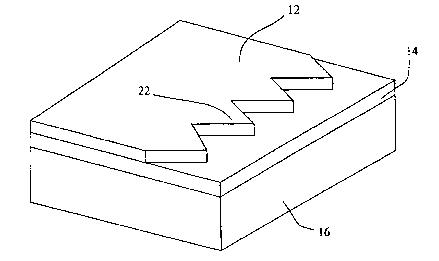
Figures 2, 3 and 4 show a first embodiment of the present invention.
The silicon wafer 16 includes a silica insulation layer 14, on top of which is
an epitaxial silicon transmissive layer 12. For clarity, the silica protective
layer 18 has not been illustrated. At the edge of the silicon transmissive
layer 12, a plurality of serrations 22 are provided. These can be formed
straightforwardly by etching the upper silicon layer by way of a suitable
mask.
Figure 3 shows the angle of the convergent sides of the serration,
marked as a.
Figure 5 shows a second example in which a is very much smaller.
The advantage of this will be apparent from the description to follow.
Figure 6 shows a third embodiment in which the serrations are
rounded, but still subtend an angle a along the roughly straight portion.
Whilst this arrangement is likely to be slightly less efficient, it may be
easier
to manufacture.
Figure 7 illustrates a principle by which the invention is considered to
work. It is necessary to consider a single serration 22 and an incoming
scattered light beam 24, arriving at an angle which is in principle random.
This will make an angle of incidence B with one edge of the serration 22,
and the beam will be internally reflected at the edge of the serration. It
will
then meet the opposite edge of the serration at an angle of B - a, i.e.
significantly less than its original angle of incidence. In the case
illustrated
in Figure 7, the angle of incidence 6 - a is less than the critical angle and
a
significant proportion of the light beam 24 will therefore escape by
refraction. Thus, the power of the reflected part of the light travelling on
CA 02336664 2001-O1-04
WO 00/02071 PCT/GB99/02012
inside the transmissive layer is strongly attenuated.
Some incident angles may result in total internal reflection at both
sides and still be reflected back into the transmissive layer. However, these
are likely to be substantially refracted out at a further edge of the chip,
particularly if the chip edges are non-perpendicular or if the serrations are
not
all aligned substantially parallel as illustrated in Figures 3, 5 and 6.
Figure 8 illustrates the advantage of decreasing a. An incoming beam
24 is still internally reflected at the first edge of the serration 22. Having
struck the first edge at a more glancing angle, B is therefore larger and, a
being smaller, 8 - a is likely to remain above the critical angle. However,
the
geometry of this situation means that the next successive reflection leaves
the beam 24 still directed toward the tip of the serration 22. As reflection
continues, B - na will eventually become less than the critical angle. Further
multiple reflections become steadily more lossy. Most of the beam may
therefore eventually couple out of the serration, but by then it will have
experienced several lossy reflections such that both the fight remaining
inside the transmissive layer and the one emitted into the device package
will be strongly attenuated.
Thus, through the present invention, a beam of stray light will be
subjected to multiple reflections at each chip edge that it meets. Undergoing
such reflective and (in particular) refractive processes will compound the
attenuation effect and result in a high total attenuation.
CA 02336664 2001-O1-04