Note : Les descriptions sont présentées dans la langue officielle dans laquelle elles ont été soumises.
CA 02336790 2001-O1-08
WO 00!73848 PCTIUS00114136
1
OPTICAL PULSE GENERATION USING A HIt~H ORDER FUNCTION
WAVEGUIDE INTERFEROMETER
Field of the Invention
The invention relates generally to the field of optical pulse generation. In
s particular, the invention relates to apparatus for narrow pulse generation
and
methods of generating narrow pulses.
Background of the Invention
Narrow optical pulse generation is required for numerous communications
and sensor systems. Narrow optical pulses are optical pulses that occupy small
ro intervals of time or optical pulses that have a steep intensity change
produced by
a control signal. in telecommunications systems, four example, the
transmission
of optical pulses is used when the modulation format requires that the
intensity
change from off to on, and then off again within a bit time period. This
produces
pulses of light, which comprise clocking or data signals.
~s Return-to-Zero (RZ) data refers to data which is either off or on for
approximately half the bit period. Non-Return-to-Zero (NRZ) data refers to
data
where the light is on or off for the whole bit period. I=lG. 1 illustrated a
prior art
timing diagram 10 of Clock 12, NRZ data 14, and R:? data format 16. Typically,
these data formats can be constructed in the electrical system by using a
logical
20 "and ing" between the data clock and the data itself.
At high data rates, it is difficult to generate poises electrically with prior
art
optical modulators. It is also difficult to generate pullses having a
predetermined
shape for the specific application such as soliton and other narrow optical
pulse
formats for very long distance propagation.
2~ There exists several prior art pulse generator's for generating narrow and
predetermined pulse formats that comprise cascaded replications of Mach-
Zehnder interferometers. These prior art devices use separately fed
controlling
CA 02336790 2001-O1-08
WO 00/73848 PCT/US00/14136
2
sections. The input signals and operating bias state of the aggregate device
is
controlled in a variety of ways depending on the design. Some of these designs
use modified input signals to each section of the aggregate device to produce
the
desired pulse train. Other prior art methods partially modulate the transfer
function of a modulator with a device, such as an electro-absorption
modulator, in
order to generate fast pulses.
There are numerous disadvantages of these prior art designs. For
example, these methods require precise control of the time delay and phase of
the different input signals, which is both difficult and costly to achieve.
Also,
io there is a relatively high power penalty associated with generating a
number of
high-speed signals and associated with the additional physical length required
for
the device.
There exists a need for an apparatus and method for generating narrow
RZ pulses for modern communications systems. There also exists a need for
~s generating pulses with a very narrow width that can be transmitted over
long
distances. There also is a need for an apparatus and method for generating a
Gaussian, or hyperbolic secant squared shape pulsE: at high speeds, which is
the
algebraic shape required for soliton pulse generation.
Summary of the Invention
2o The-present invention relates to a pulse generator comprising a high order
function waveguide interferometer that generates narrow pulses and pulses
having a predetermined shape for specific applications such as soliton and
other
narrow optical pulse formats. A principal discovery of the present invention
is
that nested and parallel configurations of interferometric modulators can be
used
2s to generate narrow pulses and pulsing having a predetermined shape for
specific
applications.
Accordingly, the present invention features an optical pulse generator
having a high order transfer function. In one embodiment, the optical pulse
CA 02336790 2001-O1-08
WO 00/73848 PCTIUS00/14136
3
generator includes a first and a second nested interferometric modulator, each
modulator comprising an optical input, an electrical input, a first arm, a
second
arm and an optical output. The second interferometric modulator is optically
coupled into the second arm of the first interferometriic modulator. The
optical
s output of the first interferometric modulator generates pulses at a
repetition rate
that is proportional to a multiple of a frequency of an electrical signal
applied to
the electrical input of at least one of the first and second interferometric
modulator and at a duty cycle that is inversely proportional to the order of
the
transfer function of the optical pulse generator. The duty cycle may be
inversely
~o non-linearly monotonically proportional to the order of the transfer
function of the
optical pulse generator. The multiple may be any integer equal to or greater
than
one. A phase modulator may be coupled in series with the output of the first
interferometric modulator to chirp the optical pulses with a modulation signal
applied to an electrical input of the phase modulator.
is )n one embodiment of the invention, the pulses generator also includes a
third interferometric modulator comprising a first and aecond arm and an
electrical
input. The third interferometric modulator has an input optically coupled to
the
output of the first interferometric modulator. The pulse generator of this
embodiment also includes a fourth interferometric modulator comprising a first
and
2o second arm and an electrical input. The fourth interferometric modulator is
optically coupled into the second arm of the third interferometric modulator.
The
optical output of the third interferometric modulator generates pulses at a
repetition rate that is proportional to a multiple of a frE:quency of an
electrical
signal applied to the electrical input of at least one of the second and the
fourth
2s interferometric modulator and at a duty cycle that is inversely non-
linearly
proportional to the order of the transfer function of thE: optical pulse
generator.
The interferometric modulators may be amplitude or phase modulators. In
one embodiment, the interferometric modulators are Mach-Zehnder modulators
formed on a lithium niobate substrate that may be X-cut or Z-cut. The
CA 02336790 2001-O1-08
WO 00/73848 PCTIUS00/1413b
4
interferometric modulators may also be substantially velocity matched or
substantially temperature compensated.
In one embodiment of the invention, the interferometric modulators are
narrow band modulators. That is, the bandwidth of the modulators is
substantially
s limited to a predetermined bandwidth. Using narrow band modulators may
increase the efficiency of the optical pulse generation. In one embodiment,
the
splitting ratio between the first and the second arm of at least one
interferometric
modulator is substantially less than one.
The present invention also features an optical pulse generator having a
~o high order transfer function that comprises a plurality of interferometric
modulators
optically connected in parallel. Each of the plurality of interferometric
modulators
includes a first and second arm and an electrical input. The optical pulse
generator having even order transfer functions includes an optical waveguide
that
is optically coupled in parallel with the plurality of interferometric
modulators. An
is optical output generates optical pulses having a repetition rate that is
proportional
to a multiple of a frequency of an electrical signal applied to the electrical
input of
at least one of the plurality of interferometric modulators and having a duty
cycle
that is inversely non-linearly proportional to the order of the transfer
function of the
optical pulse generator. The multiple may be any integer equal to or greater
than
20 one.
The output waveguide of at least one of the plurality of interferometric
modulators may include a bias electrode, wherein a voltage applied to the bias
electrode modifies a phase of an optical signal propagating from the at least
one
of the plurality of interferometric modulators. In addition, a phase modulator
may
2s be coupled in series with the output of the first interfs~rometric
modulator to chirp
the optical pulses with a modulation signal applied to. an electrical input of
the
phase modulator.
The present invention also features a method for generating optical pulses
with a high order nested interferometric modulator. The method may generate
CA 02336790 2001-O1-08
WO 00/73848 PCT/US00/14136
narrow pulses and pulses having a predetermined shape for specific
applications
such as soliton and other narrow optical pulse format,. The method includes
receiving an input optical beam and splitting the beam into a first and second
optical beam. A material propagating the first optical beam is electro-
optically
s biased, thereby changing a characteristic of the first c>ptical beam. The
electro-
optical bias may change the extinction ratio of the pulses.
The second optical beam is split into a third and fourth optical beam. A
material propagating at least one of the third and the fourth optical beams is
electro-optically biased thereby changing a characteristic of at least one of
the
~o third and the fourth optical beams. At least one of them third and fourth
optical
beams is modulated with an electrical signal. The fir;>t, third, and fourth
optical
beams are interfered to generate optical pulses having a repetition rate that
is
proportional to a multiple of a frequency of the electrical modulation signal
and
having a duty cycle that is inversely non-linearly proportional to the order
of the
~s nested interferometric modulator.
CA 02336790 2001-O1-08
WO 00/73848 PCTIUSOOI14136
6
Brief Description of the Drawings
This invention is described with particularity in the appended claims. The
above and further advantages of this invention may be better understood by
referring to the following description taken in conjunction with the
accompanying
drawings, in which:
FIG. 1 illustrates a timing diagram of Clock, NIRZ data, and RZ data
formats known to the prior art.
FIG. 2a illustrates a schematic diagram of a Nlach-Zehnder interferometer
known to the prior art.
lo FIG. 2b illustrates the transfer function betwe~ln the applied modulation
signal and the output intensity of the prior art modulator of FIG. 2a.
FIG. 2c illustrates a time domain output signal) for the Mach-Zehnder
interferometer of FIG. 2a with a sinusoidal signal applied to the input
electrode.
FiG. 3 illustrates an embodiment of a narrow pulse generator using a
is nested modulator configuration of order N=2 according to the present
invention.
FIG. 4 illustrates a transfer function between the applied modulation signal
and the output intensity of one embodiment of the narrow pulse generator of
the
present invention.
FIG. 5 illustrates a time domain output of one embodiment of the narrow
2o pulse generator of the present invention with the generator being biased at
an
intensity maximum and having an input sinusoidal modulation signal.
FIG. 6 illustrates an embodiment of a narrow pulse generator using a
nested modulator configuration of order N=3 according to the present
invention.
FIG. 7 illustrates an embodiment of a narrow pulse generator using a
2s nested modulator configuration of order N=4 according to the present
invention.
CA 02336790 2001-O1-08
WO 00/73848 PCTIUS00114136
7
FIG. 8 illustrates a general embodiment of a narrow pulse generator using
a nested modulator configuration of arbitrary order according to the present
invention.
FIG. 9 illustrates an embodiment of a narrow pulse generator using a
s cascaded configuration of nested modulator of order N=4 according to the
present invention.
FIG. 10 illustrates an embodiment of a narrow pulse generator using a
nested modulator configuration of order N=4 and a phase modulator according to
the present invention.
to FIG. 11 illustrates an embodiment of a narro4v pulse generator using a
nested modulator configuration of order N=4 and multiple phase modulators
according to the present invention.
FIG. 12 illustrates an embodiment of a narrow pulse generator using a
nested modulator configuration of order N=4 and a phase modulator positioned
in
is a passive arm of a modulator according to the present invention.
FIG. 13 illustrates a general embodiment of ~~ narrow pulse generator
using a nested modulator configuration of arbitrary order and multiple phase
modulators according to the present invention.
FIG. 14 illustrates the extinction ratio and pulse width as a function of
drive
2o power for an embodiment of a 2x20Gb/s pulse genE~rator of the present
invention.
FIG. 15a illustrates the optical output generai:ed by a 2x20Gb/s pulse
generator of the present invention for a drive power equal to 30dBm.
FIG. 15b illustrates the optical output generated by a 2x20Gb/s pulse
2s generator of the present invention for drive power equal to 27dBm.
CA 02336790 2001-O1-08
WO OOI73848 PCTlUS00/14I36
FIG. 16a illustrates the optical output generated by a 2x20Gb/s pulse
generator of the present invention for a symmetrical (bias equal to 0.2 V-pi.
FIG. 16b illustrates optical output generated by a 2x20Gbls pulse
generator of the present invention for an extinction ratio bias equal to 0.15
V-pi.
s FIG. 16c illustrates extinction ratio as a function of extinction ratio bias
for
a 2x20Gbls pulse generator of the present invention,.
FIG. 17 illustrates optical loss and pulse width as a function of drive power
for a 1 x40Gb/s pulse generator of the present invention.
FIG. 18a illustrates the optical output generatE;d by a 1 x40Gb/s pulse
io generator of the present invention for a drive power Equal to 31.75 dBm.
FIG. 18b illustrates the optical output generatE:d by a 1 x40Gbls pulse
generator of the present invention for a drive power f:qual to 27.5 dBm.
Detailed Description
A pulse generator of the present invention comprises a high order function
is waveguide interferometer that generates narrow pul:>es and pulses having a
predetermined shape for specific applications such a~,s soliton and other
narrow
optical pulse formats. There are several prior art devices that use high order
function waveguide interferometers. For example, U.S. Patent No. 5,101,450 to
Olshansky describes a parallel configuration of interferometric modulators
that is
2a used for canceling second order intermodulation distortion in analog
communications systems.
Also, in Yu Wang-Boulic, entitled A Linearized~ptical Modulator for
Reducin~c Third-Order Intermodulation Distortion, Journal of Lightwave
Technology, Vol. 10 No. 8, August {1992), a cascaded configuration of Mach-
2s Zehnder modulators is described for reducing third order intermodulation
distortion in analog communication systems. In addition, in Masayuki Izutsu et
CA 02336790 2001-O1-08
WO 00173848 PCT/US00114136
9
al., entitled, Integrated Optical SSB Modulator/Freauency Shifter", IEEE
Journal
of Quantum Electronics, Vol. QE-17, No. 11, November (1981), an analog
frequency shifter is described that comprises a paralllel configuration of
interferometric modulators. Prior art devices that use high order function
s waveguide interferometers have been limited to analog applications.
For chirp free modulation, the modulator transfer function of a high order
function waveguide interferometer can be expressed as:
E=~e~ 2e J ~ =cos"' C
(1)
where E represents the complex amplitude of the optical E-field, _ represents
~o the applied modulation, and IV represents the order: The intensity of the
light can
e_;e,, ~'-N ~ ,
I -_ I( 2 ~ cos .~ 9
be represented by:
(2)
FIG. 2a illustrates a schematic diagram of a prior art Mach-Zehnder
interferometer (MZI) 100 with order N=1. An input light signal 102 is split
into a
is, first waveguide branch 104 and a second waveguide branch 106. A modulation
signal 107 is applied to an input electrode l 08. The transfer function of the
prior
art modulator illustrated in FiG. 2a where N=1 can be expressed as:
_ eie~z +e_~B,,z ~ 8
E ~ 2 ~ - cos ( 2 l
(3}
The transfer function reduces to cos(8/Z) because tlhere is no chirp or phase
shift
2o with modulating and thus, no imaginary component in E that changes with 8.
CA 02336790 2001-O1-08
WO 00173848 PCTlUS00/14136
FIG. 2b illustrates a transfer function between the applied modulation
signal and the output intensity of the prior art Mach-:Zehnder interferometer
of
FIG. 2a. By modulating the Mach-Zehr~der interferometer 100 with a modulation
signal having a sinusoidal frequency at the input electrode 108, an output 110
of
the interferometer generates output pulses that comprise the combination of
the
sinewave input signal applied to the cosine wave traansfer function of the
interferometer 100.
FIG. 2c illustrates a time domain output signal for the prior art Mach-
Zehnder interferometer 100 of FIG. 2a with a sinusoidal modulation signal
~o applied to the input electrode 108. FIG. 2c illustrates the output signal
corresponding to a modulation signal applied over 2 Pi radians, which
corresponds to a "double sweeping" of the transfer Junction of the modulator.
The modulator 100 is biased so that the intensity is maximized with the
modulation signal turned off. The modulation signal sweeps out the transfer
is function about the intensity maximum. The signal generated has a frequency
double that of the modulation signal.
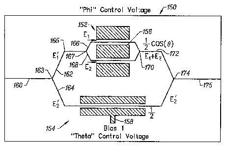
F1G. 3 illustrates an embodiment of a pulse generator 150 according to the
present invention that comprises a high order function waveguide
interferometer.
The pulse generator 150 has a fourth order response in intensity vs.
modulation
Zo signal and thus has a significantly "sharper" transfer function than the
prior art
Mach-Zehnder interferometer of Fig. 2. The pulse generator 150 comprises an
outer or first Mach-Zehnder interferometer 154 and an inner or second Mach-
Zehnder interferometer 152 in a "nested" configuration. That is, the second
interferometric modulator is optically coupled into an arm of the first
2s interferometric modulator. The inner Mach-Zehnder interferometer 152
includes
a Phi control voltage electrode 156 for applying a modulation signal. The
outer
Mach-Zehnder interferometer 154 includes a Theta control voltage electrode or
bias electrode 158 for applying a modulation signal or a bias signal.
CA 02336790 2001-O1-08
WO 00/73848 PCTNS001i4136
11
In one embodiment, metal electrodes are usE~d to provide a means of
controlling the static optical phase of the relative arrns of the inner Mach-
Zehnder
interferometer 152 and the outer Mach-Zehnder interferometer 154. The metal
electrodes 156 and 158 are also used to provide attenuation for balancing the
s light in the respective arms to produce the desired extinction of the light
in the off
state, and the desired fight output in the on state. The electrodes may be
used in
conjunction with 50% "y" branch circuits, which also have good, stable
extinction
and power balance characteristics with a minimum of temperature, wavelength,
or temporal instability.
~o Both the inner Mach-Zehnder interferometer 152 and the outer Mach-
Zehnder interferometer 154 may be formed from X-cut or Z-cut lithium niobate.
Also, both the inner Mach-Zehnder interferometer 152 and the outer Mach-
Zehnder interferometer 154 may be velocity matched or temperature
compensated interferometers. In addition, both interferometers may be narrow
is band interferometers. Using narrow band interferorneters is useful for
optimizing
the efficiency of the pulse generator.
Specifically, the pulse generator 150 includes an input waveguide 160 that
is split into a first 162 and a second waveguide 164 of the outer Mach-Zehnder
interferometer 154 at a first junction 163. The first 4nraveguide 162 is
optically
2o coupled to an input 165 of the inner Mach-Zehnder interferometer 152. The
first
waveguide 162 is split into an inner first 166 and an inner second waveguide
168
at a second junction 167. The inner first 166 and inner second waveguide 168
are then recombined at a third junction 170 to form an output waveguide 172 of
the inner Mach-Zehnder interferometer 152. The output waveguide 172 is
2s combined with the second waveguide 164 at a fourth junction 174 to form an
output waveguide 175 of the outer Mach-Zehnder interferometer 154.
In operation, an input optical signal propagai;es down the input waveguide
160, and then splits into a first and a second optical signal at the first
junction
163. The first and second optical signals propagate in the outer first 162 and
CA 02336790 2001-O1-08
WO 00/73848 PCT/USOOI14136
12
outer second waveguide 164, respectively. In one embodiment, the first and
second optical signals each have an intensity that is approximately one half
the
intensity of the input optical signal.
The first optical signal then propagates through the inner Mach-Zehnder
s interferometer 152. The first optical signal is split ini:o a first inner
and a second
inner optical signal at the second junction 167. The first and second inner
optical
signals propagate in the inner first 166 and inner second waveguide 168,
respectively. The inner Mach-Zehnder interferometer 152 modulates at least one
of the phase or amplitude of the first inner optical signal with a modulation
signal
~o applied to the Phi control voltage electrode 156. The modulation signal may
be a
sinusoid or a predetermined waveform.
The modulated first inner optical signal is combined with the second inner
optical signal at the third junction 170 to produce an inner interferometer
output,
which can be modulated from on to off. The resulting inner interferometer
output
is is combined with the second optical signal at the fourth junction 174 to
produce
an outer interferometer output. The second optical signal is modulated with a
modulation signal applied to the Theta or bias control voltage electrode 158.
The
outer interferometer output signal is a composite signal that can vary in
intensity
from on to off.
2o The transfer function for the embodiment of the pulse generator of FIG. 3
with N=2 can be represented by Equation 1 as follows:
a ae~2 +e-~e~~ '- ~ 8 1 1 e'B +e-~e ~ 1
E=~ 2 ~ -cos ~2~-_2+~~ 2 ~=2+2coslg)
(4)
The inner Mach-Zehnder interferometer 152 is represented by the _ cos(9) term
and the waveguide 164 having the bias electrode 1 ~i8 is represented by the
2s constant _ term. In this embodiment, the bias electrode 158 is used to
align the
phase of waveguide 164 with that of the inner Mach-Zehnder interferometer 152.
CA 02336790 2001-O1-08
WO 00173848 PCTIUS00/14136
13
The output intensity of the pulse generator of FIG. 3 can be described by
the following equation:
I = EZ =[ _ + - cos (8)]2 {5)
s For an embodiment of the N=2 pulse generator where the splitting ratio
between outer first waveguide 162 and outer seconcl waveguide 164 is variable,
the intensity equation has the following form:
Io2c{t~ ,F,e~ ;={F~cos {~8) + ( 1 _ F~~eos {~ ~)2i-F2~sin{8)2 ~6~
where F is the splitting ratio between E1' and E2', Theta is the phase angle
of the
ro E2' leg relative to the "inner" Mach-Zehnder output, and Phi is the phase
angle of
the inner Mach-Zehnder, impressed with the applied voltage.
In one embodiment the splitting ratio is 50%. In another embodiment, the
splitting ratio is chosen to be more than 50%, to produce a second order
maxima
in the transfer function. In this embodiment, the required modulation voltage
is
rs reduced and the width of the intensity off region is increased.
FIG. 4 illustrates a transfer function between i:he applied modulation signal
and the output intensity of the narrow pulse generator of FIG. 3. The narrow
pulse generator has a "redoubled" transfer function between the applied
modulation signal and the output intensity. Domain (points A and B represent
2o points along the transfer function such that the modulator is biased fully
on or
fully off. This corresponds with physically biasing the inner Mach-Zehnder
interferometer 152 and outer Mach-Zehnder interferometer 154 in-phase or out-
of-phase, respectfully. In order to generate a symmetric, well-behaved pulse
train, the modulator should be biased at one of thesf; domain points.
Modulation
2s about either of these domain points will produce welll-behaved non-
symmetric
pulses. Also, the voltage between the two domain points will be twice the
voltage
required to tum the inner Mach-Zehnder interferometer 7 52 on and off. This
CA 02336790 2001-O1-08
WO 00173848 PCT/US00/14136
14
voltage is referred in the art as V-pi and modulator drive voltages are
typically in
units of V-pi.
FIG. 5 illustrates a time domain output of one embodiment of the pulse
generator of the present invention with the generator being biased at an
intensity
s maximum and having an input sinusoidal modulation signal of lOGHz. The
resulting output signal has a pulse width that is approximately 12
picoseconds,
with a repetition rate of approximately 20 GHz.
In one embodiment of the present invention, the transfer function is swept
when the generator is biased at an intensity maximum, thereby doubling the
~o output frequency, as described in connection with FIG. 2c. When the input
optical signal is symmetrical about an intensity maximum, two intensity pulses
are generated for every cycle of the input signal, hence frequency doubling
the
pulse rate of the optical output, with respect to the modulation signal.
For the embodiment illustrated in FIG. 3, the input frequency is 1 OGHz,
~s which when doubled, produces a 20 GHz optical clock frequency. Also, for
the
embodiment shown in FIG. 5, the pulse width facilitates splitting and
recombining, to produce 12.5 picosecond pulses, which can be used for 40 Gb/s
data transmission.
In another embodiment of the invention, the marrow pulse generator
-- ZO comprises a plurality of inner Mach-Zehnder interferometers in a
"nested"
structure. The nested structure can have any number of inner Mach-Zehnder
interferometers in order to achieve
the desired output intensity characteristics: For example, for order N=3,
Equation
1 can be expressed as:
p,~e~~ ~~-P 'girl ~ ; ~ ~ (?''~8~7 .~ p ~'~B» .;( PiB~'' +P-iBf7. ~
F,_-~ 2 ~ =ccx ~'~~4~ 2 ~+QI- 2 ~=4cc~~ 2 +4cr» 2
CA 02336790 2001-O1-08
WO 00173848 PCTlUS00/14136
(7)
FIG. 6 illustrates a pulse generator 200 of the present invention having
order N=3. The first inner Mach-Zehnder interferometer 202 represents the _
cos
(8/2) term and the second inner Mach-Zehnder interferometer 204 represents the
cos (38/2) term in Equation 7. The pulse generator 200 includes the two inner
Mach-Zehnder interferometers 202 and 204, and an outer Mach-Zehnder
interferometer 206. The outer Mach-Zehnder interferometer 206 also includes a
bias electrode 208 for applying a modulation signal.
In one embodiment, electrodes are used to control the static optical phase
ro of the relative arms of the first inner Mach-Zehnder interferometer 202,
the
second inner Mach-Zehnder interferometer 204, and the outer Mach-Zehnder
interferometer 206. The electrodes can change the amplitude of the light in
the
waveguide by causing a predetermined amount of excess optical loss due to
loading of the optical signal by the metal. The loading occurs when the tail
of the
rs optical beam in the waveguide comes in contact with the metal electrode.
This
loading generally occurs when there is no dielectric material (referred to as
a
buffer layer) between the metal and the edges of the waveguide.
In one embodiment, the electrodes 240 and 242 of Mach-Zehnder
interferometers 202 and 204, respectively, and the bias electrode 208, are
biased
2o to balance or change the fraction of the light in the relative arms to
produce the
desired extinction in the off state and the desired light output in the on
state. The
electrodes in this embodiment are used in conjunction with 75% "y" branch
circuits 210, 212 or couplers, which have desired extinction and power balance
properties.
2s Both the inner Mach-Zehnder interferometers 202 and 204 and the outer
Mach-Zehnder interferometer 206 may be formed from X-cut or Z-cut lithium
niobate. Afso, both the inner Mach-Zehnder interferometers 202 and 204 and the
outer Mach-Zehnder interferometer 206 may be velocity matched interferometers
or temperature compensated interferometers. !n addition, both the inner Mach-
CA 02336790 2001-O1-08
WO OOI73848 PCT/US00114136
16
Zehnder interferometers 202 and 204 and the outer (Mach-Zehnder interferometer
206 may be narrow band interferometers. Using narrow band interferometers is
useful for optimizing the efficiency of the poise geneirator.
Specifically, the pulse generator 200 includes an input waveguide 214 that
is split into a first 216 and a second waveguide 218 of the outer Mach-Zehnder
interferometer 206 at a first junction 210. Junction 210, in one embodiment,
is a
75% optical coupler. The first waveguide 2i 6 is optically coupled to a first
input
223 of the first inner Mach-Zehnder interferometer 202. The first input 223 is
split
into a first inner first 224 and a first inner second waveguide 226 at a
second
io junction 225. The first inner first 224 and first inner second waveguide
226 are
then recombined down stream of the first inner Mach-Zehnder interferometer 202
at a third junction 232 to form a first output waveguide 233 of the first
inner Mach-
Zehnder interferometer 202.
The second waveguide 218 is optically coupled to a second input 227 of
is the second inner Mach-Zehnder interferometer 204. The second input 227 is
split into a second inner first 228 and a second inner second waveguide 230 at
a
fourth junction 229. The second inner first 228 and the second inner second
waveguide 230 are then recombined at a fifth junction 234 to form a second
output waveguide 235 of the second inner Mach-Zehnder interferometer 204.
2o The first output waveguide 233 is combined with a :>econd output waveguide
235
at a sixth junction 212 to form an output waveguide 237 of the outer Mach-
Zehnder interferometer 206. Junction 212 in one embodiment is a 75% "y"
branch coupler.
In operation, an input optical signal propagates down the input waveguide
2s 214, and then splits into a first and a second opticall signal at the first
junction
210. The first and second optical signals propagate in the outer first 216 and
outer second waveguide 218, respectively. In one embodiment, the first and
second optical signals have a splitting ratio that is approximately 75%.
CA 02336790 2001-O1-08
WO 00/73848 PCT/US00/14136
77
The first optical signal then propagates through the first inner Mach-
Zehnder interferometer 202. The first optical signal its split into a first
inner and a
second inner optical signal at the second junction 22:5. The first and second
inner optical signals propagate in the first inner first 224 and first inner
second
s waveguide 226, respectively. The first inner Mach-Zehnder interferometer 202
modulates at least one of the phase or amplitude of the first inner optical
signal
with a modulation signal applied to its electrode 240.. The modulation signal
may
be a sinusoid or a predetermined waveform. The modulated first inner optical
signal is combined with the second inner opticai signal at the third junction
232 to
to produce a first inner interferometer output, which can be modulated from
onto
off.
The second optical signal is split into a third and fourth inner optical
signal
at the fourth junction 229. The third and fourth inner optical signals
propagate in
the second inner first 228 and the second inner second waveguide 230,
is respectively. The second inner Mach-Zehnder interiferometer 204 modulates
at
least one of the phase or amplitude of the fourth inner optical signal with a
modulation signal applied to its electrode 242. The modulation signal may be a
sinusoid or a predetermined waveform. The moduia~ted fourth inner optical
signal
is combined with the third inner optical signal at the 'fifth junction 234 to
produce a
20 second inner interferometer output, which can be modulated from on to off.
The resulting first and second inner interferonneter outputs are combined
at the sixth junction 212 to produce an outer interferometer output. The
second
interferometric output signal is modulated with a modulation signal applied to
the
bias control voltage electrode 208. In one embodiment, a signal is applied to
the
2s bias electrode 208 that aligns the phase of the two inner Mach-Zehnder
interferometers, thereby substantially canceling the phase shift across the
couplers. The bias points of the two inner Mach-Zehnder interferometers can
also be controlled relative to one another. The outer interferometer output
signal
is a composite signal that can vary in intensity from ~on to off.
CA 02336790 2001-O1-08
WO 00/73848 PCTlUS00lI4I36
18
FIG. 7 illustrates a pulse generator 250 of the present invention having
order N=4. In this embodiment, Equation 1, can be Expressed as
eiBl2 +e-iA'2 a -t a ~ ~''~B +e ~~B ~ B 'g -~G'
E=~ 2 ~ =,cos ~~~-R( 2 ~+2( 2 -~+~-Rcosl281+2cosf8l+~
(8)
The pulse generator 250 includes three inner Mach-;?ehnder interferometers
280,
282, and 274, and outer Mach-Zehnder interferometer 300. The outer Mach-
Zehnder interferometer 300 also includes an inner bias electrode 276 and an
outer bias electrode 292 for applying bias and modullation signals. The
constant
term (3/8) in Equation 8 represents the inner bias. T'he 118 cos (28) term
represents the first inner modulator 280 and the - cos (8) term represents the
first
~o outer Mach-Zehnder interferometer 282.
In one embodiment, electrodes are used to control the static optical phase
of the relative arms of the first inner Mach-Zehnder interferometer 280, the
second inner Mach-Zehnder interferometer 282, the third inner Mach-Zehnder
interferometer 274, and the outer Mach-Zehnder interferometer 300. The
is electrodes of Mach-Zehnder interferometer 280 and 282 and the two bias
electrodes 276 and 292 are also used to balance or change the fraction of the
light in the relative arms to produce the desired extinction in the off state
and the
desired light output in the on state. The electrodes in this embodiment are
used
in conjunction with 75% "y" branch circuits 258, 298 ~or couplers, which have
2o desired extinction and power balance properties.
The first inner Mach-Zehnder interferometer 2.80, the second inner Mach-
Zehnder interferometer 282, the third inner Mach-Zelhnder interferometer 274,
and the outer Mach-Zehnder interferometer 300 may be formed from X-cut or Z-
cut lithium niobate. Also, the Mach-Zehnder interferometers 280, 282, and 274
2s and the outer Mach-Zehnder interferometer 300 may be velocity matched
interferometers or temperature compensated. The Mach-Zehnder
interferometers 280, 282, and 274 may also be narrow band interferometers.
CA 02336790 2001-O1-08
WO OOI73848 PCT/US00I14136
19
Narrow band interferometers are useful for optimizing the efficiency of the
pulse
generator.
Specifically, the pulse generator 250 includes an input waveguide 252 that
is split into a first 254 and a second waveguide 256 of outer Mach-Zehnder
interferometer 300 at a first junction 255. Junction 255, in one embodiment is
a
balanced optical coupler. The first waveguide 254 is optically coupled to a
second junction 258. In one embodiment, the second junction is a 75% "y"
branch circuit. The second junction 258 comprises an input to the third inner
Mach-Zehnder interferometer 274.
~o The first waveguide 254 is split into a first inner waveguide 262 and a
second inner waveguide 260. The first inner waveguide 262 is optically coupled
to input 264 of first inner Mach-Zehnder interferomelter 280. The first inner
waveguide 264 is split into a first inner first 268 and a first inner second
waveguide 266 at a third junction 267. The first innE~r first 268 and first
inner
is second waveguide 266 are then recombined at a fourth junction 270 to form a
first inner output waveguide 272 of the first inner Mach-Zehnder
interferometer
280. The second inner waveguide 260 and the first inner output waveguide 272
are optically coupled to a fifth junction 298. In one embodiment, the fifth
junction
comprises a 75% "y" branch circuit. First outer output waveguide 278 is
optically
Zo coupled to the output of fifth junction 298.
The second waveguide 256 is optically coupled to input 284 of second
inner Mach-Zehnder interferometer 282. The input ;?84 is split into a second
inner first waveguide 288 and a second inner second waveguide 286 at a sixth
junction 287. The second inner first 288 and the second inner second waveguide
2s 286 are then recombined at a seventh junction 290 'to form a second output
waveguide 294 of the second inner Mach-Zehnder interferometer 282. The first
output waveguide 278 is combined with a second output waveguide 294 at an
eighth junction 296 to form an output waveguide 29'7 of the outer Mach-Zehnder
interferometer 300.
CA 02336790 2001-O1-08
WO 00/"13848 PCTIUS00114136
In operation, an input optical signal propagates down the input waveguide
252, and then splits into a first and a second optical signal at the first
junction
255. The first and second optical signals propagate in the outer first 254 and
outer second waveguide 256, respectively. In one embodiment, the first and
second optical signals each have an intensity that is approximately one half
of
the intensity of the input optical signal.
The first optical signal propagates through junction 258 which splits the
first optical signal into a first inner and a second inner optical signal. The
second
inner optical signal propagates to third junction 267 which splits the second
inner
to optical signal into a third inner optical signal and a fourth inner optical
signal. The
third and fourth inner optical signals propagate in first inner second 266 and
a
first inner first waveguide 268, respectively. The first inner Mach-Zehnder
interferometer 280 modulates at least one of the phase or amplitude of the
third
inner optical signal with a modulation signal applied to its electrode 281.
The
is modulation signal may be a sinusoid or a predetermiined waveform. The
modulated third inner optical signal is combined with the fourth inner optical
signal at the fourth junction 270 to produce a first inner interferometer
output,
which can be modulated from on to off. The first inner optical signal
propagates
through second inner waveguide 260 and is combined with the first inner
2o interferometer output at fifth junction 298 to produce a third inner
interferometer
output signal. The third inner interferometer output ;>ignal is modulated with
a
modulation signal applied to the bias electrode 276. The third inner
interferometer output signal is optically coupled through fifth junction 298
to first
outer output waveguide 278 to produce a first outer iinterferometer output
signal
2s with can be modulated from on to off.
The second optical signal propagates through outer second waveguide
256 to the input 284 of second inner Mach-Zehnder interferometer 282, and
eventually to sixth junction 287. Sixth junction 287 splits the second optical
signal into a fifth inner optical signal and a sixth inner optical signal. The
fifth and
3o sixth inner optical signals propagate in second inner second 286 and a
second
CA 02336790 2001-O1-08
WO 00/73848 PCT/USOOI14136
21
inner first waveguide 288, respectively. The second inner Mach-Zehnder
interferometer 282 modulates at least one of the phase or amplitude of the
fifth
inner optical signal with a modulation signal applied to its electrode 283.
The
modulation signal may be a sinusoid or a predetermiined waveform. The
s modulated fifth inner optical signal is combined with the sixth inner
optical signal
at the seventh junction 290 to produce a second outer interferometer output
signal, which can be modulated from on to off.
The resulting first and second outer interFeronneter output signals are
combined at the eighth junction 296 to produce an outer interferometer output
to signal. The second outer interferometer output signal is modulated with a
modulation signal applied to the bias control voltage electrode 292. The bias
electrode 292 aligns the phase of the inner Mach-Ze~hnder interferometers and
the second inner waveguide 260, thereby canceling the phase shift across the
couplers. The bias points of the inner Mach-Zehnder interferometers can also
be
~s controlled relative to one another. The outer interferometer output signal
is a
composite signal that can vary in intensity from on to off.
FIG. 8 illustrates a pulse generator having N nested interferometric
modulators. Boxes 352 and 354 represent some combination of "y" branch
circuits and couplers or other power dividing structures to achieve the
desired
2o split ratio for each branch. Numerous other passive power splitting
structures
known in the art, such as Multi-Mode Interference (MM!) structures, or even
bulk
optic power splitting arrangements, such as tensing systems can also be used.
Mach-Zehnder interferometers 356, 360, and 364 modulate the various
optical signals propagating in the pulse generator 3;i0. The bias electrodes
358,
2s 362, and 3fi6 align the phase of the various arms of the nested modulator.
For a
given order, not all multiples of /2 show up as drive levels in the
architecture.
For example, order N=3 contains modulation levels 3 /2 and 12, whereas order
N=4 contains levels 2-and - In addition, the constant term representing the
passive waveguide arm appears only for the even orders (i.e. N= 2, 4,...).
CA 02336790 2001-O1-08
WO 00173848 PCT/US00/14136
22
Another discovery of the invention is that higher order transfer functions
can also be achieved by cascading two or more IvwE>r order nested modulators.
The number of cascaded nested modulators will depend on the number of
modulation signals that must be applied; the strength of the required
modulation,
s and the complexity of the bias control, which is typically controlled
actively, using
a feedback loop. For example, cascading two N=2 order modulators creates the
same transfer function as one N=4 modulator, with both arrangements requiring
two modulation signals. However, cascading four N:=1 modulators to produce the
same function is less practical, as four time-synchronized modulation signals
~o must be applied, instead of two.
FIG. 9 illustrates a cascaded configuration of two N=2 order nested
modulators 456 of the present invention. This configuration has the same
transfer function as an N=4 order modulator. Modulator 150 includes an inner
Mach-Zehnder interferometer 152 and an outer Maclh-Zehnder interferometer
is 154 in a nested configuration. Outer Mach-Zehnder interferometer 154 has an
input waveguide 160 and an output waveguide 175. Output waveguide 175 is
optically coupled to an input waveguide 160' of a second modulator 150'.
Modulator 150' is identical in form and function to modulator 150, except that
the
input waveguide 160' of modulator 150' receives the output optical signal of
2o modulator 150, instead of an external optical signal.
In operation, an input optical signal propagates down the input waveguide
160 of Mach-Zehnder interferometer 150. After splitting at the first junction
163,
the signal propagates through Mach-Zehnder interferometer 150. The signal is
then recombined at the fourth junction 174. The connbined signal then enters
2s input waveguide 160' of modulator 150' where it encounters the fifth
junction
163'. After splitting at fifth junction 163', the signal propagates through
MZI 150'
and recombines at the eighth junction 174'. The resulting output signal
corresponds to the output of an N=4 order modulator.
CA 02336790 2001-O1-08
WO 00/73848 PCTIUS00114136
23
In one embodiment of the present invention, the modulators are chirped.
That is, the frequency of the optical signals shift with the applied
modulation. The
equation for the transfer function for chirped operation includes a term
containing
a complex component, which would represent the phase shift with modulation.
/ ie~'-
E-[ a 2e ~ ~,,»e ~zos"~~8~e"'a
s Comlbining Equation 1 with a complex term yields:
where the value of m depends on the strength of the chirp desired.
FIG. 10 illustrates an embodiment of a chirped pulse generator 370 for
order N=4. The chirped generator includes phase modulator 372 positioned in
to the output of outer Mach-Zehnder interferometer 30(). The characteristics
of the
chirp are determined by applying a modulation signal to electrode 374 of phase
modulator 372.
FIG. 11 illustrates a chirped pulse generator 380 for order N=4. FIG. 11
also has a similar architecture to the embodiment shown in FIG. 7, except that
~s phase modulators 382, 386, and 390 have been adcled to waveguides 260',
272',
and 294', respectively. The chirp characteristics can be manipulated by
applying
modulation signals to electrodes 384, 388, and 392. The phase modulators 382,
386, and 390 in one embodiment, can induce equal amounts of phase
modulation into each arm.
2o FIG. 12 illustrates a pulse generator of the present invention that uses an
unbalanced push-pull design in the inner Mach-Zehnder interferometers. This
design integrates the phase modulation function with the amplitude modulation
function. FIG. 12 has a similar architecture to the ernbodiment shown in FIG.
7,
except that phase modulator 382 is added to waveguide 260'.
CA 02336790 2001-O1-08
WO 00/73848 PCT/US00114136
24
The degree of asymmetry is different in the tlAlO inner Mach-Zehnder
interferometers, 280 and 282, since Mach-Zehnder interferometer 280 must be
driven twice as hard as the Mach-Zehnder interferometer 282 because of the
scaling required in the cosQ terms. As a result of this, the waveguide arms of
s Mach-Zehnder interferometer 280 also will be modulated twice as hard as the
arms of Mach-Zehnder interferometer 282. HowevE:r, since the net phase shift
at
the output of Mach-Zehnder interferometers 280and 282 must be matched,
Mach-Zehnder interferometer 280 has less asymmetry in order to compensate for
the doubled drive level. One advantage of this embodiment is that all of the
to modulation structures are in parallel. Such a configuration results in
reduced
space, due to the finite length of the phase modulator electrodes.
FIG. 13 illustrates an Nt" order chirped pulse generator. The phase
modulation and biasing functions are integrated into the electrodes 422, 424,
and
426 as shown. Alternatively, the phase modulation and biasing electrodes can
~s be separate electrodes. In another embodiment, a;>ymmetrical electrodes are
used for integrating phase modulation into the inner Mach-Zehnder
interferometers.
The pulse generator of the present invention is particularly useful for
generating narrow digital logic "RZ" pulses. The pulse generator of the
present
2o invention is also particularly useful for generating signals having a point
of
inflection in a desired output characteristic, such th<~t the output transfer
function
has a broad region of no output intensity with respect to the controlling
signal.
Such signals produce an enhanced output on/off state and are advantageous for
creating optimized onloff extinction.
2s The narrow pulse generator of the present invention may be further
understood by an example of the performance of an embodiment of the present
invention. The narrow pulse generator of the present invention enables the
transmission of data at 40 Gbls. The invention could be used in 1 40Gb/s
(straight-40) system architectures or 2 20Gb/s systems. The pulse generator in
CA 02336790 2001-O1-08
WO 00/73848 PCT/US00/14136
one embodiment is intended to be used in an optical time-domain multiplexed
(OTDM) system architecture.
FIG. 14 illustrates extinction ratio and pulse width versus RMS power for
an embodiment of the present invention. As shown, a stream of 12 ps-wide {40
s Gb/s pulse width) pulses separated by 50 ps (20 Gb.Js pulse period) can be
generated using an embodiment of the nested Mach-Zehnder device. This is
accomplished by modulating around the biased ON state (Point A in FIG. 4) of
the modulator using a frequency of lOGHz and a volltage of four times V-pi.
FIG.
14 illustrates both the extinction ratio 450 and the pulse width 452 as a
function
~o of RF drive power for an embodiment of the invention. The extinction ratio
450 is
maximized at four times V-pi drive voltage (~30dBm), while the pulse width is
approximately 12 ps (which is 24% of the pulse reps~tition period, or
l2ps/50ps).
This embodiment requires a drive voltage of four times V-pi voltage in order
to
extinguish all signal in the OFF state. Inadequate drive voltage will result
in a
~s non-zero signal in the OFF state of the modulator and a broadening of the
pulse
but will not affect the peak optical pulse power.
FIG. 15a and FIG. 15b illustrates a 2 20 Gb/s pulse generator driven with
+30 dBm and +27 dgm. In one embodiment, the nested modulator configuration
of the present invention requires both the inner and outer modulators to be
2o biased ON for optimal operation. The bias of the inner interferometer,
sometimes
referred to as the symmetry bias, affects the spacing of adjacent pulses as
shown in FIG. 16a for a symmetrical bias offset of 0..2 V-pi. The bias of the
outer
interferometer affects the extinction ratio of the pulsf: generator and is
often
called the extinction ratio (ER) bias. FIG. i 6b illustrates the optical
output for a
2s modulator with an offset in ER bias. FIG. 1 fic illustrates the extinction
ratio as a
function of ER bias voltage in units of V-pi. In one embodiment, bias control
is
achievable since optimal biasing is achieved when both the inner and outer
Mach-Zehnder interferometers are biased in the ON state.
CA 02336790 2005-10-18
The 2x20 Gb/s pulse generator can be used to create a 1 x40 Gb/s pulse
stream by biasing the device in the OFF state (Point B in FIG. 4) and
modulating it
with a frequency of 20 GHz. Used in this mode, the effect of decreasing the
drive
power results in an increase in the optical loss of the device and a decrease
in the
optical pulse width while the extinction ratio remains relatively a function
of drive
power. The four times V-pi drive power of one embodiment of the pulse
generator
operated at a 20 GHz drive frequency is +33.6 dBm which is relatively high.
However, normal operation of the device in a 1 x40 Gb/s pulse mode would
require
the modulator to be modulated with a voltage less than four times V-pi.
The pulse width 460 and excess optical loss 462 as a function of drive power
for the 1 X40 Gb/s pulse generator of one embodiment of the present invention
is
illustrated in FIG. 17. Twelve-picosecond-wide pulses can be achieved at a
drive
power of +31.75 dBm. The optical power penalty for this drive power is 0.8 dB.
The
corresponding pulse width and optical power penalty at +27.5 dBm are 10.1 ps
and
6.0 dB, respectively. FIG. 18a and 18b show the optical output for +31.75 dBm
and
+27.5 dBm input powers, respectively.
One advantage of the nested modulator configuration of the present
invention for use as a 1 X40 Gb/s pulse generator is that it can provide
extremely
short pulses of approximately 11 ps-13 ps without sacrificing optical
throughput.
One embodiment of the present invention has less than 2 dB excess optical
loss.
The pulse generators of the present invention can include an
interferometric modulator having a compensation network as described in U.S.
patent number 6,483,953 entitled, "External Optical Modulation Using Non-Co-
Linear
compensation Networks," which is commonly owned by the present assignee. The
compensation network is electrically coupled to the electrical waveguide at a
junction.
The compensation network propagates the electrical signal in a second
direction of
propagation that is substantially non-collinear with the first direction of
propagation.
In one embodiment, the compensation network includes at least
26
CA 02336790 2001-O1-08
WO 00!73848 PCTNSOOI14136
27
one of an all-pass electrical network, an inductor-capacitor "Pi" network,
traveling
wave coupler, filter, and transmission line transformer.
The compensation network is designed to modify at least one of the phase
or the amplitude of the electrical signal at the junction relative to the
phase or the
amplitude of the optical signal at the junction, respectively, and then return
the
modified electrical signal to the electrical waveguide~. The compensation
network
may be a time delay network or a phase delay network.
One advantage of the compensation network; of the present invention is
that the electrical loss per unit length can be designed to be significantly
Power
~o than the electrical loss per unit length of the electrical waveguide to
minimize RF
losses. Another advantage of the compensation network is that it may be
removably attached to the electro-optic device so that it can be replaced by
another compensation network. Another advantagE; of the compensation network
is the temperature dependence of the compensation network can be made to be
~s inversely proportional to the temperature dependence of the electro-optic
material so as to compensate for temperature non-linearities in the electro-
optic
material.
In one embodiment, the compensation network is a phase delay network
that modifies the phase of the electrical signal so that a phase difference
2o between the electrical signal and the optical signal at the junction
relative to the
phase difference between the electrical signal and irhe modulation on the
optical
signal at an input to the optical waveguide is reduced or is substantially
zero. In
another embodiment, the compensation network is a phase delay network that
modifies the phase of the electrical signal at the junction relative to the
phase of
2s the modulation on the optical signal at the junction Iby a predetermined
delay that
is variable over a range from zero to one hundred and eighty degrees. In this
embodiment, the phase of the electrical signal at the junction relative to the
phase of the modulation on the optical signal at the junction may be modified
to
be substantially one hundred and eighty degrees.
CA 02336790 2001-O1-08
WO 00173848 PCT/US00/14136
28
in operation, each of the plurality of compensation networks modifies a
phase of the electrical signal at a respective junction of the plurality of
junctions
relative to a phase of the modulation on the optical signal at the respective
junction by a predetermined delay and then returns 'the modified electrical
signal
to the electrical waveguide. The predetermined delay is variable over a range
from zero to one hundred and eighty degrees and in one embodiment of the
invention, the predetermined delay is substantially one hundred and eighty
degrees. tn another embodiment, each compensation network modifies the
phase of the electrical signal at the respective junction relative to the
phase of the
lo modulation on the optical signal at the respective junction so that the
electrical
signal is substantially in-phase with the modulation on the optical signal at
each
of the plurality of junctions.
Equivalents
While the invention has been particularly shown and described with reference
to
~s specific preferred embodiments, it should be understood by those skilled in
the
art that various changes in form and detail may be made therein without
departing from the spirit and scope of the invention as defined by the
appended
claims.