Note : Les descriptions sont présentées dans la langue officielle dans laquelle elles ont été soumises.
CA 02337659 2001-02-20
CC Byers 33-6-6
BACKPLANE CONFIGURATION WITHOUT COMMON SWITCH FABRIC
FIELD OF THE INVENTION
The present invention generally relates to large electronic systems, and in
particular, to a telecommunications switching system configuration that does
not
require a common switch fabric board.
BACKGkOUND OF THE INVENTION
Large electronic systems, as used in computing, data networking, and
telecommunications elements often use a common backplane to provide high speed
interconnection between several circuit boards, packs or modules that plug
into slots in
1o the backplane. The backplane is typically constructed of a multi-layer
circuit board
with conductive traces selectively routed to provide the high-speed
interconnection.
Connectors are provided on the backplane to couple circuit boards, packs, or
modules
which are held in place using a slotted chasis. The properties of these
backplanes often
have large influence over the capacity, performance, reliability, cost, and
scale
15 properties of electronic systems. Some backplane designs provide high
capacity, while
others provide low cost.
Currently, there are two predominant architectures for providing backplane
transport infrastructures in high-speed telecommunications platforms, the bus
and the
fabric. These architectures both have limitations preventing the creation of a
truly
2o universal platform.
Bus-based backplanes use; a large set of parallel signals, where each signal
typically touches each slot and hence each board. This interconnection scheme
is
versatile and low cost, but imposes practical limits of a few billion bits per
second on
the maximum system throughput and also limits reliability. The total
throughput must
25 also be shared among all boards on the backplane. Buses are typically used
in smaller
systems that do not process large amounts of broadband traffic, or in systems
with
severe cost constraints. In particular, bus-based backplanes have a very low
cost of
CA 02337659 2001-02-20
CC Byers 33-6-6 2
common elements, and therefore permit low system costs, especially where a
system is
not equipped with all of its circunt cards or modules initially.
Fabric based systems use a central high-speed fabric or hub to switch traffic.
between all modules. High-speed point-to-point connections (either parallel or
serial)
are routed over a cable or backplane between each module and the central
fabric, in a
star topology. The central fabric can provide the large bandwidths (over 1
trillion bits
per second) needed to support high-speed computing or broadband
communications.
Unfortunately, because the full central fabric, with support for the maximum
number of
connections, must be installed before any modules can be interconnected, the
cost of
such a system is often quite high; especially for partially equipped systems,
where the
large cost of the fabric is only amortized over a few modules.
Computing and telecomrrmnications needs are increasing tremendously. In
particular, high bandwidth systems are considered a necessity for distributed
computing, networking and telecommunications switching. In light of the
shortcomings of traditional bus-based backplane systems and central fabric-
based
systems, a need exists for a new paradigm in backplane-based systems that has
the low
cost of bus-based interconnect and the high capacity of central fabric-based
interconnect.
SUMMARY OF THE INVENTION
2o An electronic interconnection system in accordance with the present
invention
includes a backplane. The backplane includes a mufti-layer circuit board with
a
plurality of connectorized slots for connecting to traces routed in the
backplane. Using
the connectorized slots, circuit packs are coupled to the backplane and traces
routed
therein. To facilitate communication among the circuit packs coupled to the
backplane,
a hub circuit is provided on each circuit pack. In addition, point-to-point
connections
are provided from one slot in the backplane to each and every other slot in
the
backplane. The point-to-point connections are made using traces in the
backplane. The
hub circuits on each circuit pack couple to the point-to-point connections to
facilitate
CA 02337659 2001-02-20
CC Byers 33-6-6 3
control and routing over the comrnunication links formed by the point-to-point
connections.
The point-to-point connections formed in the backplane can be selectively
routed between the slots, either physically or virtually, using the hub
circuit to provide
:> different connection topologies, capacity, and reliability. In one
configuration, each
slot includes a point-to-point connection to all other slots, creating a full
mesh. For
example, for a backplane with sixteen slots for circuit boards, each board has
fifteen
point-to-point connections, each terminating at a different slot. This
configuration
provides a direct point-to-point connection from any one circuit pack or
module to
io another circuit pack or module. In addition, communication between circuit
packs is
readily facilitated by communication through another circuit pack, if for
example, a
point-to-point connection is faulty or unavailable. A myriad of other
configurations are
contemplated, including a ring configuration, wherein adjacent slots have
point-to-point
connections and slots at opposite ends are joined via point-to-point
connections to
15 complete the ring.
BRIEF DESCRIPTION OF THE DRAWINGS
FIG. 1 is a block diagram of a backplane-based interconnection system in
accordance with the present invention.
FIG. 2 is a block diagram of a circuit board for use in the backplane-based
2o interconnection system shown in FIG. l .
FIG. 3 is a block diagram ~of a backplane-based interconnection system in
accordance with the present invention wherein circuit boards are connected in
a ring
topology.
FIG. 4 is a block diagram .of a backplane-based interconnection system in
25 accordance with the present invention wherein circuit boards, are connected
in a double
star topology.
CA 02337659 2001-02-20
CC Byers 33-6-6 4
FIG. 5 is a block diagram of a backplane based interconnection system in
accordance with the present invention wherein multiple backplanes are
connected using
ext;,nder boards.
BRIEF DESCRIPTION OF THE PREFERRED EMBODIMENTS
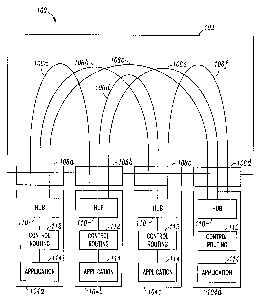
FIG. 1 is a block diagram of a backplane interconnection system 100 in
accordance with the present invention. System 100 includes a backplane 102 and
several circuit boards 104a-d. Backplane 102 provides intercommunication
between
circuit boards 104a-d. In particular, in accordance with the present
invention, circuit
boards 104a-d each have point-to~-point connections 106a-f, which are used to
route
to communications between circuit boards 104x-d.
Backplane 102 has slots 108a-d, which provide the interface for circuit packs
104a-d to couple to point-to-point connections 106a-f. Slots 108a-d are
preferably
connectors. Point-to-point connections 106a-f are formed by conductive traces
formed
in the multiple layers of backplane 102. In the preferred embodiment, the
electrical
properties of point-to-point connections 106a-f are implemented in accordance
with the
InfiniBand standard from the InfiniBand Trade Association, 5440 SW Westgate
Drive,
Suite 217, Portland, OR 97221 (www.sysio.org). In accordance with the
InfiniBand
electrical signaling specification, point-to-point connections 106a-f are 2.5
gigabits per
second bi-directional serial links over metallic conductors. As an alternative
to
2o InfiniBand, any suitable substitute; point-to-point link technology can be
used. Most
preferably, the traces forming point-to-point connections 106a-f are routed as
signal
pairs with the signal pairs routed adjacent to each other on a single layer of
the mufti
layer backplane, or on adjacent layers using identical conductor geometries.
Most
preferably, the layers adjacent to the layers carrying signal pairs are power
or ground
2~ (that is, signal ground).
Each of the circuit boards 104a-d includes a hub circuit 110, a
control/routing
circuit 112 and an application circuit 114. Hub circuit 110 directly
interfaces with
point-to-point connections 106a-f to allow the circuit board to communicate
over the
CA 02337659 2001-02-20
CC Byers 33-6-6 5
point-to-point connections. Control/routing circuit 112 implements the
protocol to
control the routing over hub circuit I 10 to the point-to-point connections
106a-f.
Application circuit 114 includes the circuitry necessary to implement a
particular
application and interface that application to the interconnection system 100.
For
example, application circuit I 14 may implement an access or line interface,
such as
ISDN or a feeder or trunk interface, such as TI, T3 or OC12. Also, application
circuit
114 may implement a processing; resource, a digital signal processor or
another
resource.
Although four circuits boards 104a-d are shown in FIG. 1 only the physical
uo limitations of backplane 102 and point-to-point connections 106a-f limit
the number of
circuit boards in an interconnection system in accordance with the present
invention. In
a preferred embodiment, 16 slots are provided in backplane 102 and 240 point-
to-point
links are provided in backplane 102 to provide a point-to-point, full duplex
connection
between all 16 slots in the backp:lane.
5 FIG. 2 is a block diagram showing circuit board 104a in additional detail.
Circuit board 104a includes a power circuit 116, hub circuit I 10,
control/routing circuit
I 12 and application circuit 114. Power circuit 116 obtains power from
backplane 102
and preferably conditions, converts and distributes that power to the
components of
circuit board 104a. Hub circuit I 10, control/routing circuit 112 and
application circuit
ao 114 implement the functions described above and further below.
Hub circuit 110 preferably includes an NxN hub switch 120 and a routing table
122. Hub circuit 110 serves as a distributed fabric switch element. This is in
contrast
to a central fabric switch used in telecommunications systems in the prior
art. NxN hub
switch 120 couples circuit board 104a to N minus one point-to-point
connections in the
as backplane. For system 100 shown in FIG, l , N equals four. NxN hub switch
120
accepts and routes traffic to N links. Most preferably, one of the N links is
circuit
board 104a. The other links are t:he point to point connections to other hub
circuits on
circuit boards in other slots. NxN hub switch 120 has N minus one external
links to
CA 02337659 2001-02-20
CC Byers 33-6-6 6
point-to-point connections in bac;kplane 102 and one internal link 124 coupled
to
control/routing circuit I 12. Hub circuit 110 accepts traffic from the
external links and
routes it to the internal link. Also, hub circuit 110 receives communications
from
circuit board 104a over internal link 124 and routes the communication to one
or more
appropriate external links. A further function of hub circuit 110 is to accept
traffic
from one of the external links and route that traf~'ic to some other of the
external links
without ever terminating that tra:Ffic on circuit board 104a. Routing table
122 is
preferably a memory element that stores configuration information and other
data
related to the point-to-point connections coupled to hub circuit I 10_
Control/routing circuit I 12 provides some control over the communications
implemented by hub circuit 110 .and also interfaces application circuit 114 to
hub
circuit I 10. Control/routing circuit 112 preferably includes a control
processor 126 and
a buffer 128. Control processor 126 is preferably any microprocessor, memory
and
necessary interface circuits. Control processor 126 preferably implements a
host
adapter function that provides low level control, buffering and priority
management in
an InfiniBand network. Also, control processor 126, which may be a network
processor, preferably provides message and packet processing functions used
for
example in IP routing, asynchronous transfer mode (ATM) switching, and time
slot
interchange and protocol adaptation. Control processor 126 preferably
translates and
2o interfaces traffic from hub circuit I 10 to the buses used on application
circuit 114. For
example, application circuit 114 may include one or more serial links, or
busses,
including an InfiniBand serial link, a PCI bus, the UTOPIA bus (used for
asynchronous
transfer mode cells), and the H. l XO bus (used for synchronous timeslots).
Buffer 128
is preferably a large RAM that stores packets, messages and other payloads
being
a:5 processed by control processor 126.
Application circuit 114 v<~ries depending upon the application to be
implemented. To facilitate flexibility and modularity, application circuit 114
includes
several connectors 130 for receiving circuit board modules with varying
functionality.
CA 02337659 2001-02-20
CC Byers 33-6-6 7
Application circuit 114 includes an application processor 132, RAM 134, and
peripherals 136. Application processor 132 uses RAM 134 and peripherals 136 to
implement an application, for example, an access or trunk interface or a
feeder interface
in a telecommunications network. Application processor 132 is coupled to
control
processor 126 over bus 13 8. The preferred implementation for bus 13 8 is a
standardized bus such as PCI or a serial link such as InfiniBand. Other
standard
interface buses 140, 142 are coupled to connectors 130 for application
circuits utilizing
those buses. Most preferably, connectors 130 are PCI mezzanine card sockets.
In
addition to the other functions listed above, application processor 132
preferably
1~:~ includes functions for bandwidth management, call processing or a general-
purpose
server.
FIG. 3 illustrates a backplane interconnection system 200 in accordance with
the present invention. System 200 is similar in most respects to system 100 of
FIG. 1,
as noted by the reuse of the same reference numerals used to designate
components of
l:i system 100. However, the point-to-point connections 1068 j in backplane
202 are
configured differently from the point-to-point connections 106 a-f in
backplane 102. In
particular, the point-to-point connections 106g j are selectively routed to
form a ring
configuration. In this ring configuration adjacent circuit boards have point-
to-point
connections to each other. For example, circuit board 104b has point-to-point
20 connections 106g, 106h to adjacent circuit boards 104a and 104c. The two
circuit
boards at opposite ends of the system, circuit boards 104a and 104d, are
considered to
be adjacent and have a point-to-point connection 106j between them. Although
illustrated in FIG. 3 as physical point-to-point connections, point-to-point
connections
106g-j are alternatively virtual connections that may, for example, be
implemented with
25 direct or indirect connections, such as point-to-point connections 106a-f
of FIG. 1.
FIG. 4 illustrates a backplane interconnection system 300 in accordance with
the present invention. System 300 is similar in most respects to system 100 of
FIG. 1,
as noted by the reuse of the same reference numerals used to designate
components of
CA 02337659 2001-02-20
CC Byers 33-6-6 8
system 100. However, the point-to-point connections 106k-o in backplane 202
are
routed differently from the point-to-point connections 106a-f in backplane
102. In
particular, the point-to-point connections 106k-o are selectively routed to
form a double
star configuration. In this double star configuration, two of circuit boards
104a-d are
arbitrarily chosen to be central circuit boards. In FIG. 4, circuit boards
104a, 104d are
used as central circuit boards. The circuit boards that are not central
circuit boards, in
this case circuit boards 104 b, 104c, have point-to-point connections 106k,
106n, 1061,
106o to each of the central circuit boards, but no point-to-point connections
to each
other. The central circuit boards 104a, 104d have a point-to-point connection
106m
to between them. The point-to-point connections 106k-o may be virtual
connections. An
alternative to the double star configuration is a single star configuration,
in which one
circuit board is designated a cenl:ral circuit board and every other circuit
board has a
point-to-point connection to the central circuit board, but no point-to-point
connection
to the other circuit boards.
t5 FIG. 5 illustrates a configuration of two backplane interconnection systems
in
accordance with the present invention. One system is designated system 500 and
the
other system is designated 500'. Both systems 500, 500' include circuit boards
104a-c
and backplanes 102 as shown and discussed above with respect to FIG. 1. In
accordance with the present invention, system 500 and system 500' are coupled
together for communication between the circuit boards on each system by
extender
boards 504. Extender boards 504 are coupled to backplanes 102 to extend the
point-to-
point connections in the backplanes 102. Preferably, extender boards 504 are
passive
circuit boards with traces routed therein to electrically extend the traces in
the
backplanes 102. One or more cables or connectors 506 are preferably used to
~5 electrically couple the systems 500, 500' to each other.
A myriad of systems may utilize the backplane interconnection system
disclosed herein. One of many example systems is a universal gateway that
provides
conversions from one network to another network. In a universal gateway
CA 02337659 2001-02-20
CC Byers 33-6-6 9
implemented using a backplane interconnection system in accordance with the
invention, the application circuits may implement access circuits and digital
signal
processing circuits. For example, some application circuits may terminate
access lines
and long haul trunks. The interfaces utilized may include digital subscriber
line (DSL)
interfaces or OC 12 trunk interfaces or other line or trunk interfaces. The
digital signal
processing circuits may be used for compression, decompression, encryption and
decryption.
The present invention provides an interconnection system that includes a
backplane with connectorized slots and a plurality of point-to-point
connections
between the slots. The point-to-point connections are controlled by hub
circuits
coupled to each slot of the backplane. The point-to-point connections and the
distributed switching function provided by the hub circuit eliminate the need
for a
central fabric switching board. 'hhis advantageously reduces costs while not
sacrificing
bandwidth and capacity.
:~5 Whereas the present invention has been described with respect to specific
embodiments thereof, it will be understood that various changes and
modifications will
be suggested to one skilled in thf; art and it is intended that the invention
encompass
such changes and modifications as fall within the scope of the appended
claims.