Note : Les descriptions sont présentées dans la langue officielle dans laquelle elles ont été soumises.
CA 02338539 2001-01-24
WO 00/07301 PCT/US99/17081
HARDWARE-EFFICIENT TRANSCEIVER WITH
DELTA-SIGMA DIGITAL-TO-ANALOG CONVERTER
BACKGROUND OF THE INVENTION
1. Field of the Invention
This invention relates to communications systems. Specifically, the
present invention relates to transceivers used in communications networks.
II. Description of the Related Art
Cellular telecommunications systems are characterized by a plurality
of mobile transceivers in communication with one or more base stations.
Each transceiver includes a transmitter and a receiver.
In a typical transceiver, an analog radio frequency (RF) input signal,
received by an antenna, is downconverted by an RF section to an
intermediate frequency (IF). Signal processing circuits perform noise
filtering and adjust the magnitude of the signal via analog automatic gain
control (AGC) circuitry. An IF section then mixes the signal down to
baseband and converts the analog signal to a digital signal. The digital
signal
is then input to a baseband processor for further signal processing to output
voice or data.
Similarly, the transmitter receives a digital input from the baseband
processor and converts the input to an analog signal. This signal is then
filtered and upconverted by an IF stage to an intermediate frequency. The
gain of the transmit signal is adjusted and the IF signal is upconverted to RF
in preparation for radio transmission.
In both the transmit and receive sections, signal gain adjustment and
mixing is typically performed in the analog domain. This necessitates the
use of a plurality of local oscillators (LOs) for signal downconversion,
upconversion, and mixing. Analog local oscillators tend to be bulky and
require the use of one or more phase-locked loops. As is well known in the
art, phase-locked loops are large, expensive circuits that consume a
CA 02338539 2001-01-24
WO 00/07301 PCTIUS99/17081
2
considerable amount of power. Hence the use of PLLs, drive up the cost,
size and power consumption of analog local oscillators and the transceivers
in which these circuits are employed.
Hence, a need exists in the art for a cost-effective, space-efficient
transceiver with low noise characteristics and minimal power consumption.
SUMMARY OF THE INVENTION
The need in the art is addressed by the transceiver of the present
invention. The inventive transceiver includes a digital circuit for
converting baseband signals to intermediate frequency signals. A signal
source provides a first periodic signal of a first frequency. A direct digital
synthesizer provides a second periodic signal of a second frequency from the
first periodic reference signal. An upconverter circuit digitally upconverts
the baseband signals to digital intermediate frequency signals using the
second periodic signal. A digital-to-analog converter converts the digital
intermediate frequency signals to analog intermediate frequency signals
using the first periodic signal.
In the transceiver implementation, the digital circit upconverts a first
transmit signal from a first frequency to a second frequency in response to
the second periodic signal and provides a digital transmit signal in response
thereto. A second circuit is provided for converting the digital transmit
signal to an analog transmit signal. Transmit and receive circuitry are
provided for transmitting the analog transmit signal and receiving an
analog receive signal, respectively.
In a specific embodiment, the analog receive signal is digitally
downconverted to provide a digital receive signal in response to a second
periodic signal. A significant feature of the invention resides in the
provision of the first and second periodic signals with a single local
oscillator. A direct digital synthesizer is included for generating one of the
reference signals from the output of the local oscillator.
The transmit circuit includes a delta-sigma digital-to-analog converter
having the first periodic signal as an input. The delta-sigma digital-to-
CA 02338539 2009-11-18
74769-317
3
analog converter has a low-bit digital-to-analog converter and a delta-sigma
modulator.
In the illustrative embodiment, the low-bit digital-to-analog converter
is a 1-bit digital-to-analog converter and the delta-sigma modulator is a
sixth order
delta-sigma modulator. The delta-sigma modulator includes amplifiers with
approximately the following gains: 3/2, -3/4, 1/8.
The transmit circuit includes a digital automatic gain control circuit for
adjusting the gain of the first signal. An output of the automatic gain
control circuit
is input to the delta-sigma digital-to-analog converter. Also, a digital
lowpass filter,
a digital mixer, and a digital adder are included in the transmit circuit. An
output of
the digital adder provides an input to the automatic gain control circuit.
The novel design of the present invention is facilitated by the
elimination of a local oscillator via the use of the direct digital
synthesizer and the
delta-sigma digital-to-analog converter. By eliminating a local oscillator,
power
and space savings are achieved.
According to one aspect of the present invention, there is provided a
digital circuit for converting baseband signals to intermediate frequency
signals
comprising: a signal source for providing a first periodic signal of a first
frequency;
frequency synthesizing means for providing a second periodic signal of a
second
frequency from said first periodic signal; upconverting means for digitally
upconverting baseband signals to digital intermediate frequency signals using
said
second periodic signal; and digital-to-analog converter means for converting
said
digital intermediate frequency signals to analog intermediate frequency
signals
using said first periodic signal.
According to another aspect of the present invention, there is
provided a digital circuit for converting intermediate frequency signals to
baseband
signals comprising: a signal source for providing a first periodic signal of a
first
frequency; frequency synthesizing means for providing a second periodic signal
of
a second frequency from said first periodic signal; downconverting means for
CA 02338539 2009-11-18
74769-317
3a
digitally downconverting analog intermediate frequency signals to digital
baseband
signals using said second periodic signal; and analog-to-digital converter
means
for converting said analog intermediate frequency signals to digital
intermediate
frequency signals using said first periodic signal.
According to still another aspect of the present invention, there is
provided a transceiver comprising: a receive circuit; a transmit circuit; a
signal
source for providing a first periodic signal of a first frequency; frequency
synthesizing means for providing a second periodic signal of a second
frequency
from said first periodic signal; a baseband processor connected to said
receive
circuit and said transmit circuit; a digital circuit in said transmit circuit
for converting
baseband signals from said baseband processor to digital intermediate
frequency
signals using the second periodic signal; and a delta-sigma digital-to-analog
converter in said transmit circuit for converting said digital intermediate
frequency
signals to analog intermediate frequency signals using the first periodic
signal.
According to yet another aspect of the present invention, there is
provided a transceiver comprising: first means for digitally upconverting a
first
signal from a first frequency to a second frequency in response to a first
reference
signal and providing a first digital signal in response thereto; second means
for
converting said first digital signal at said second frequency to a first
analog signal;
third means for transmitting said first analog signal; fourth means for
receiving a
second analog signal; fifth means for digitally downconverting said second
analog
signal to a second digital signal in response to a second reference signal;
and a
phase-locked loop for providing said first and said second reference signals.
According to a further aspect of the present invention, there is
provided a transceiver comprising: first means for generating a first periodic
signal
of a first frequency; second means for digitally generating a second signal of
a
second frequency from said first periodic signal; third means for using said
first
periodic signal to perform digital-to-analog conversion or analog-to-digital
conversion of signals in a transmit circuit or a receive circuit of said
transceiver,
said third means including a delta-sigma modulator; and fourth means for
utilizing
said second signal for an additional circuit in said transceiver and/or said
receiver,
CA 02338539 2009-11-18
74769-317
3b
said additional circuit requiring a clock signal or reference frequency
control signal,
said clock signal or said reference frequency control signal provided by said
second signal.
According to yet a further aspect of the present invention, there is
provided a transceiver comprising: means for generating a first periodic
signal of a
first frequency; means for receiving an analog signal, said receiving means
including means for utilizing said first periodic signal to convert said
received
analog signal to a digital signal; means for digitally processing said
received signal
and for providing a first transmit signal; means for transmitting said first
transmit
signal, said means for transmitting including means for utilizing said first
periodic
signal to convert said first transmit signal from digital to analog; and means
for
driving digital circuitry in said means for transmitting and/or said means for
receiving with said first periodic signal.
According to still a further aspect of the present invention, there is
provided a high performance, space-efficient and power-efficient transceiver
comprising: antenna means for receiving and transmitting radio frequency
signals;
first translating means for translating said radio frequency signals to
intermediate
frequency signals and vise versa; second translating means for translating
said
intermediate frequency signals to baseband signals and visa versa, said second
translating means having a single local oscillator; filtering means for
removing
undesirable signals from said baseband signals and said intermediate frequency
signals; gain control means in communication with said filtering means for
adjusting the gain of said baseband signals and said intermediate frequency
signals to facilitate signal processing; and means for processing said
baseband
signals in accordance with predetermined transceiver instructions.
According to another aspect of the present invention, there is
provided a high performance, hardware-efficient transceiver comprising:
antenna
means for receiving receive signals and transmitting transmit signals;
oscillator
means for generating a first periodic signal; a signal processor for
processing
transmitted signals and received signals; a receive circuit having a first
analog-to-
digital converter having said first periodic signal as an input for converting
said
CA 02338539 2009-11-18
74769-317
3c
receive signals to baseband signals, said baseband signals input to said
signal
processor; a transmit circuit having a mixing circuit for mixing transmit
baseband
signals received from said signal processor to intermediate frequency band
signals; a direct digital synthesizer for synthesizing a second periodic
signal from
said first periodic signal for clocking said mixing circuit; a first digital-
to-analog
converter in said transmit circuit having said first periodic signal as an
input for
converting signals of said intermediate frequency band to analog signals; and
a
translating circuit for translating said intermediate frequency band signals
to a
frequency band suitable for broadcast and generating said transmit signals in
response thereto.
According to yet another aspect of the present invention, there is
provided a digital circuit for translating signals between an intermediate
frequency
band and baseband comprising: a local oscillator for providing a first
periodic
signal of a first frequency; a delta-sigma converter for converting analog
signals to
digital signals and/or visa-versa using said first periodic signal; a direct
digital
synthesizer for providing a second periodic signal based on said first
periodic
signal, said second periodic signal having a second frequency; and mixing
means
for translating said digital signals and/or said analog signals between said
intermediate frequency band and said baseband using said second periodic
signal.
According to another aspect of the present invention, there is
provided a method for transmitting and receiving signals including the steps
of:
digitally upconverting a first signal from a first frequency to a second
frequency in
response to a first reference signal and providing a first digital signal in
response
thereto; converting said first digital signal at said second frequency to a
first analog
signal; transmitting said first analog signal; receiving a second analog
signal;
digitally downconverting said second analog signal to a second digital signal
in
response to a second reference signal; and providing said first and said
second
reference signals via a local oscillator.
CA 02338539 2009-11-18
74769-317
3d
BRIEF DESCRIPTION OF THE DRAWINGS
The features, objects, and advantages of the present invention will
become more apparent from the detailed description set forth below when taken
in
conjunction with the drawings in which like reference characters identify
correspondingly throughout and wherein:
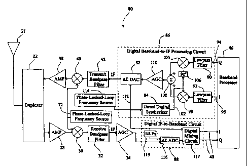
FIG. 1 is a block diagram of a prior art transceiver.
FIG. 2 is a block diagram of a transceiver constructed in accordance
with the teachings of the present invention and employing a delta-sigma (Al)
digital-to-analog converter (DAC) and a direct digital synthesizer (DDS).
FIG. 3 is a block diagram of the DE DAC of FIG. 2.
CA 02338539 2001-01-24
WO 00/07301 PCT/US99/17081
4
DETAILED DESCRIPTION OF THE PREFERRED
EMBODIMENTS
While the present invention is described herein with reference to
illustrative embodiments for particular applications, it should be
understood that the invention is not limited thereto. Those having
ordinary skill in the art and access to the teachings provided herein will
recognize additional modifications, applications, and embodiments within
the scope thereof and additional fields in which the present invention
would be of significant utility.
The following review of a traditional transceiver is intended to
facilitate an understanding of the present invention.
FIG. 1 is a block diagram of a prior art transceiver 20. The transceiver
is a dual conversion telecommunications transceiver and includes an
15 antenna 21 for receiving and transmitting RF signals. A duplexer 22
connected to the antenna 21 facilitates the separation of receive RF signals
24
from transmit RF signals 26.
The receive RF signals 24 enter a receive circuit that includes a
receive RF amplifier 28, an RF-to-IF mixer 30, a receive bandpass filter 32,
an
20 analog receive automatic gain control (AGC) circuit 34, and an analog IF-to-
baseband processing circuit 36. The receive RF signals 24 are amplified by
the receive amplifier 28, mixed to intermediate frequencies via the RF-to-IF
mixer 30, filtered by the receive bandpass filter 32, gain-adjusted by the
receive AGC 34, and then converted to digital baseband signals 48 via the
analog IF-to-baseband processing circuit 36. The digital baseband signals 48
are then input to a digital baseband processor 46.
The RF transmit signals 26 arrive at the duplexer 22 from a transmit
circuit that includes a transmit RF amplifier 38, an IF-to-RF mixer 40, a
transmit bandpass filter 42, and analog baseband-to-IF processing circuit 44.
Digital baseband processor output signals 50 are received by the analog
baseband-to-IF processing circuit 44 where they are converted to analog
signals, mixed to IF signals that are then filtered by the transmit bandpass
filter 42, mixed up to RF by the IF-to-RF mixer 40, amplified by the transmit
amplifier 38 and then transmitted via the duplexer 22 and the antenna 21.
CA 02338539 2001-01-24
WO 00/07301 PCT/US99/17081
Both receive and transmit circuits are connected to the digital
baseband processor 46 that processes the received baseband digital signals 48
and outputs the digital baseband processor output signals 50. The baseband
processor 46 may include such functions as signal to voice conversions
5 and/or vise versa.
The baseband processor output signals 50 are 90 out of phase with
respect to each other and correspond to in-phase (I) and quadrature (Q)
signals. The output signals 50 are input to digital-to-analog converters
(DACs) 52 in the analog baseband-to-IF processing circuit 44 where they are
converted to analog signals that are then filtered by lowpass filters 54 in
preparation for mixing. The signals' phases are adjusted, mixed, and
summed via a 90 shifter 56, baseband-to-IF mixers 58, and adder 60,
respectively. The adder 60 outputs IF signals 62 that are input to an analog
transmit automatic gain control (AGC) circuit 64 where the gain of the
mixed IF signals 62 is adjusted in preparation for filtering via the transmit
bandpass filter 42, mixing up to RF via the IF-to-transmit mixer 40,
amplifying via the transmit amplifier 38, and eventual radio transmission
via the duplexer 22 and the antenna 21.
The DACs 52 in the baseband-to-IF processing circuit 44 are clocked by
a first local oscillator (LO1) 66. The sampling rate of the DACs 52 is
determined by the frequency of the local oscillator 66. The local oscillator
66
also provides the clock signal to the analog IF-to-baseband processing circuit
36, which is used by analog-to-digital converters (ADC) 68 in the analog IF-
to-baseband processing circuit 36.
A second local oscillator (L02) 70 is required by the mixers 58 in the
analog-to-baseband processing circuit 44. The second local oscillator 70
outputs a clock signal having a different frequency than the output of the
first local oscillator 66. Typically, the second local oscillator 70 operates
at a
much higher frequency than the first local oscillator 66.
A third local oscillator 72 is required for the operation of the receive
RF-to-IF mixer 30 and the transmit IF-to-RF mixer 40. Typically the same
local oscillator 72 is used for both mixers 30, 40.
CA 02338539 2001-01-24
WO 00/07301 PCTIUS99/17081
6
A fourth local oscillator 73 is used by an analog mixing circuit 75 in
the analog IF-to-Baseband circuit 36 to facilitate IF-to-baseband processing
functions performed by the analog mixing circuit 75.
All of the local oscillators 66, 70, 72, 73 require one or more phase-
locked loops (PLLs). PLLs are typically large analog circuits that consume
excess power.
Design limitations of the transceiver 20 limit the amount of signal
processing that can be performed in the digital domain, and require the use
of additional large analog power-consuming circuits such as local oscillators
and analog AGCs. For example, the multi-bit DACs 52 are implemented
before the analog signal mixing and filtering performed by the baseband-to-
IF-processing circuit 44. This is partly because the DACs 52 would generate
an extraordinary amount of spurious noise if they were implemented after
mixing. This is because the IF signals 62 are higher frequency signals that
magnify converter glitches thereby increasing spurious noise. The spurious
noise is typically in-band and is difficult to filter via conventional means.
Since the digital-to-analog conversion must take place before
baseband-to-IF conversion by the circuit 44, the baseband-to-IF processing
circuit 44 must be implemented in the analog domain. The analog mixers
58, filters 54, adder 60, and the analog AGC 64 are much larger and consume
more power than their digital counterparts. Furthermore, imbalances due
to low precision of analog circuits causes feedthrough of the oscillator
signal
70, which cannot be filtered by practical means.
In addition, the design of the transceiver 20 necessitates the use of at
least three local oscillators, i.e., the first local oscillator 66, the second
local
oscillator 70 and the third local oscillator 72. The oscillators 66, 70, and
72
include large, power-inefficient analog PLLs.
FIG. 2 is a block diagram of a transceiver 80 constructed in accordance
with the teachings of the present invention. The transceiver 80 employs a
delta-sigma (DE) digital-to-analog converter (DAC) 82 and a direct digital
synthesizer (DDS) 84. In the transceiver 80, the analog baseband-to-IF
processing circuit 44 of FIG. 1 and the analog IF-to-baseband processing
circuit 36 of FIG. 1 are replaced with a re-designed baseband-to-IF processing
CA 02338539 2001-01-24
WO 00/07301 PCT/US99/17081
7
circuit 86, and re-designed IF-to-baseband processing circuit 88,
respectively.
The replacements eliminate the need for the second local oscillator 70 of
FIG. 1, greatly reducing transceiver power consumption and size.
The AE DAC 82 can convert digital IF signals to analog signals
without the spurious noise problems of a multi-bit DAC. By employing the
YEA DAC 82, baseband-to-IF signal processing may be performed in the digital
domain, thus eliminating oscillator feedthrough.
The digital baseband-to-IF processing circuit 86 includes a first digital
lowpass filter 90 and a second digital lowpass filter 92 that filter
undesirable
signals such as noise from quadrature (Q) 94 and in-phase (I) 96 signals
received from the baseband processor 46, respectively. The filtered in-phase
signals are input to a first digital mixer 98, while the filtered quadrature
signals are input to a second digital mixer 100. The first mixer 98 is clocked
by a DDS clock signal 102 from the DDS 84. The DDS clock signal 102 is
shifted in phase by 90 by a digital phase shifter 106, providing a shifted
clock
signal 104 in response thereto. By clocking the mixers 98, 100 with clock
signals that are 90 out of phase, the I and Q signals are brought in phase.
The mixers 98, 100 convert the I and Q signals to IF signals that are
combined via a digital adder 108. The added IF signals are then output to a
digital AGC 110, the construction of which is well known in the art. The
digital AGC 110 adjusts the gain of the IF signals and outputs these signals
to
the Al DAC 82. The DE DAC 82 converts these signals to analog signals in
preparation for more filtering by the bandpass filter 42, mixing up to radio
frequencies by the mixer 40, amplifying by the amplifier 38 and transmitting
via the duplexer 22 and the antenna 21.
The Al DAC 82 utilizes an oscillator signal 112 generated by a single
local oscillator 114 to drive a 1-bit DAC included in the DE DAC 82 (as
discussed more fully below). The oscillator signal 112 is also used as a
frequency control signal to drive the DDS 84 that synthesizes the DDS clock
signal 102. The DDS clock signal 102 has a different frequency than the
oscillator signal 112.
CA 02338539 2009-11-18
74769-317
8
The DDS 84 produces a digitized sinusoidal signal corresponding to
the clock signal 102 from the oscillator signal 112 by accumulating phase
increments of the digitized sinusoidal signal 102 at the higher rate of the
oscillator signal 112. The accumulated phase is converted to the digitized
sinusoidal signal 102 via a look-up table (not shown). The digitized
sinusoidal signal 102 is used as a frequency reference by the mixers 98, 100
to
translate the baseband signals 94, 96 to IF.
Construction of the DDS 84 is known in the art and described in U.S.
Patent No. 4,965,533, entitled DIRECT DIGITAL SYNTHESIZER DRIVEN
PHASE LOCK LOOP FREQUENCY SYNTHESIZER, assigned to the assignee
of the present invention.
Those skilled in the art will appreciate that the DDS 84 may be
implemented as a programmable DDS whose output clock signal 102 is
adjustable in response to transmission or reception errors due to oscillator
frequency drift and/or other related errors. Such error measurements may
be detected by logic in the baseband processor 46 or via additional error
detection circuits (not shown).
Use of the DDS 84 to generate the DDS clock signal 102 eliminates the
need for an additional local oscillator with an additional PLL. The DDS 84 is
much smaller than a local oscillator and PLL and may be readily
implemented in a compact very large scale integration (VLSI) circuit along
with the digital mixers 98, 100, filters 90, 92, adder, 108, AGC 110, and DE
DAC 82. In addition, the DDS 84 consumes relatively small amounts of
power. Also, use of the low noise AZ DAC 82 eliminates the need for an
additional multi-bit DAC as is required in the transceiver 20 of FIG. 1.
With reference to FIGS. 1 and 2, the separate PLL oscillator 70 required
in the conventional transceiver 20 for baseband-to-IF conversion is
replaced, in the transceiver 80 of the present invention by the digital DDS
84.
The performance of the baseband-to-IF processing circuit 44 of FIG. 1 is
improved upon, in the present invention. In the present invention, analog
processing functions are implemented in digital circuits and the spurious
multi-bit DACs 52 are replaced with the 1-bit sigma-delta DAC 82.
CA 02338539 2009-11-18
74769-317
9
processing functions are implemented in digital circuits and the spurious
multi-bit DACs 52 are replaced with the 1-bit sigma-delta DAC 82.
In the present specific embodiment, the oscillator signal 112 is also
used to clock a digital IF-to-baseband processing circuit 88 in the receive
circuit. In the present specific embodiment, the digital IF-to-baseband
processing circuit 88 that includes a high-speed DE analog-to-digital
converter (ADC) 116, a digital mixing circuit 117, and a frequency multiplier
for converting the frequency of the oscillator signal 112 to a second
frequency for use by the AE ADC 116. The construction of AE ADCs, digital
mixing circuits, and frequency multipliers is well known in the art.
In the present embodiment, the frequency multiplier 117 divides the
frequency (Fs) of the oscillator signal 112 by four and provides the resulting
divided oscillator signal as a clock to a 1-bit ADC (not shown) included in
the AE ADC 116.
The oscillator signal 112 provides a reference frequency to the digital
mixing circuit 117 for use by the digital mixing circuit 117 to downconvert
digital IF signals output from the Al ADC 116 to the baseband signals 48.
Those skilled in the art will appreciate that digital downconversion
functions performed in the digital IF-to-baseband processing circuit 88 may
be implemented in a manner similar to up-conversion functions performed
in the digital baseband-to-IF processing circuit 86. Also, the analog AGC 34
may be implemented as a digital AGC after the EO ADC 116 in the digital IF-
to-baseband circuit 88.
Construction of the receive circuit may be implemented in accordance
with the teachings of U.S. Patent Application Serial No. 08/987,306, filed on
December 9, 1997, entitled RECEIVER WITH DELTA-SIGMA ANALOG-TO-
DIGITAL CONVERTER, assigned to the assignee of the present invention.
Those skilled in the art will appreciate that digital IF-to-baseband
processing circuit 86 may be replaced with a different version, such as the
analog IF-to-baseband processing circuit 36 of FIG. 1 without departing from
the scope of the present invention. Also, the DDS 84 of the digital baseband-
CA 02338539 2001-01-24
WO 00/07301 PCTIUS99/17081
to-IF processing circuit 86 may be implemented in the IF-to-baseband
processing circuit 88 in addition to or instead of being implemented in the
digital baseband-to-IF processing circuit 86. That is, the DDS output 102 may
be used by downconversion circuitry and/or ADCs in the IF-to-baseband
5 processing circuit 88. In addition, the AGC circuit 110 may be implemented
in the analog domain after the AE DAC 82 without departing from the scope
of the present invention.
FIG. 3 is a block diagram of the Al DAC 82 of FIG. 2. The AZ DAC 82
includes a 1-bit DAC 120 at the output of a DE modulator 122. The Al
10 modulator 122 is a sixth order AE modulator. The AE modulator 82 has
three basic building blocks 124, also termed second order resonators,
cascaded together. Each basic building block 124 includes a combination of
digital delays (z-') 128, amplifiers 130 having voltage gains a; (where i is
an
integer index ranging from 0 to 5), an adder 132, and a subtractor 134. The
adder 132 receives as parallel inputs, outputs from the amplifiers 130. One
of the amplifiers 130 has an input provided by a digital delay 128 whose
input is also the input of the other amplifier 130. This input is provided by
a digital delay 128 in a subsequent resonator 124, or, in the case of the
output
basic block 124, provided by the noise-shaped output 127 of the DE
modulator 82.
The first basic building block 124 receives the output of the digital
AGC 110 of FIG. 2 as a third input to the adder 132. Subsequent building
blocks 124 receive outputs of the previous basic building blocks 124 as third
inputs to the adders 132.
Those skilled in the art will appreciate that methods for constructing
the basic building blocks 124 are well known in the art and may be
implemented using programmable gate arrays.
The output of the adder 132 provides an input to the subtractor 134.
The output of the adder 132 is sent through a digital delay 128, providing the
output of the resonator 124. The output of the resonator 124 is sent through
another digital delay 128 and provides a second input to the adder 132
forming a feedback loop.
CA 02338539 2001-01-24
WO 00/07301 PCTIUS99/17081
11
Quantization noise is modeled as a linear noise element 126 and
occurs before the noise shaped output 127.
The voltage gains of the amplifiers 130 are picked to provide a noise
transfer function and signal transfer function that enable the AE modulator
82 to meet stability noise shaping requirements for a particular application.
Methods for picking of the gains a for the amplifiers 130 are well known in
the art. In the present specific embodiment, the gains are: a0 = 0, a, = 3/2,
a2
=0,a3=-3/4,a4=0,a5 =1/8.
The 1-bit DAC 120 is clocked by the oscillator signal 112 of FIG. 2.
Those skilled in the art will appreciate that the 1-bit DAC 120 may be
replaced by a low-bit DAC such as a 2 or 3 bit DAC without departing from
the scope of the present invention. The constructions of sigma-delta DACs
and ADCs are well known in the art.
Thus, the present invention has been described herein with reference
to a particular embodiment for a particular application. Those having
ordinary skill in the art and access to the present teachings will recognize
additional modifications, applications and embodiments within the scope
thereof.
It is therefore intended by the appended claims to cover any and all
such applications, modifications and embodiments within the scope of the
present invention.
WHAT IS CLAIMED IS: