Note : Les descriptions sont présentées dans la langue officielle dans laquelle elles ont été soumises.
CA 02338867 2001-O1-29
1
CIRCUIT ARRANGEMENT AND METHOD FOR RECEIVING AND
TRANSMITTING DATA
High level data link controller are employed for data transmission at
network interworkings in communication systems, particularly switching
systems.
These HDLC controllers are arranged at network interworkings such as, for
example,
between a network with a synchronous data transmission and a network with an
asynchronous data transmission. the selection of a data transmission rate or
of a time
slot width in a frame-oriented data transmission is prescribed by the
transmission
speed of the network interworking units. A time slot width was previously pre-
set -
1 o with the assistance of marked fields. This, however, results in the
disadvantage that
the data transmission can only be implemented in the time slots marked
therefor.
United States Letters Patent No. 5,619,500 discloses an HDLG controller
with a frame division with a fixed plurality of channels. This HDLC
controller,
however, exhibits the disadvantage that the plurality of channels as well as
the
channel width thereof within the frame cannot be changed.
The invention is based on the object of specifying a circuit arrangement
and a method that eliminates the aforementioned disadvantage.
Achieving this object derives from the features of patent claims 1, 2 and 6,
7.
2 0 The invention yields the advantage that all time slots of a transmission
frame can be used for the transmission of data.
The invention yields the advantage that the channel number for an HDLC
controller can be modified by modification of configuration parameters.
Further characteristics are recited in the subclaims.
2 5 The circuit arrangement and the method can be seen from the following,
more detailed explanation of exemplary embodiments on the basis of drawings.
Shown are:
Figure 1 a schematic illustration of a transmission link;
Figure 2 a structure of a transmission frame;
3 0 Figure 3 a schematic structure of an HDLC controller;
CA 02338867 2001-O1-29
la
Figure a block circuit diagram of an HDLC reception
4 unit;
Figure a block circuit diagram of an HDLC transmission
unit;
Figure a more detailed illustration of an FiDLC
6 reception unit; and
5 Figure a more detailed illustration of an HDLC
7 transmission unit.
CA 02338867 2001-O1-29
2
Figure 1 shows a network configuration of a data transmission link. This
network configuration is composed of a data network AD for asynchronous data
transmission and of at least one data network SD for synchronous data
transmission.
The data network AD for asynchronous data transmission can, for example, be an
ATM network, an integer network, a Datex-P network or an Ethernet. For
example,
PCM systems or a synchronous transfer mode STM can be employed for the
synchronous data transmission in the data networks SD. Respective high level
data
link controllers HDLC are arranged at the interfaces between the synchronously
and
asynchronously operating data network SD or, respectively, AD. A plurality of
data
terminal devices TL can be connected to a network termination point NT of the
synchronously operating data network SD. One or more time slots or,
respectively,
time channels are allocated to a data terminal device TL for data transmission
between
the network termination point NT and the interface between the data networks
AD,
SD.
Figure 2 reproduces a transmission frame of a PCM transmission system
as employed in the data network SD with synchronous data transmission. This
PCM
transmission frame is, for example, 16 bits long and can be subdivided into a
maximum of 16 time slots or, respectively, channels. The smallest possible
time slot
can cover one bit and the largest time slot can cover 16 bits. The bits of the
2 0 transmission frame are consecutively numbered from 0 to 15. The first time
slot TS
having the time slot width TSB of 3 bits comprises the time slots TS or,
respectively,
channels 0, 1 and 2 combined to form a data transmission channel. The
designation
of the respective time slot TS ensues with the number of the first channel at
the
beginning of the time slot TS. The first time slot is assigned the number of
the first
2 5 bit. In the following, second time slot TS, which covers the channels 3,
4, 5 and 6, the
second time slot TS has the time slot number corresponding to the number of
the first
bit of the second time slot TS. The third and fourth time slot is referenced
TS7 and
TSB.
Figure 3 shows the structure of a high level data link controller HDLG
3 0 This HDLC controller essentially comprises an HDLC receiver unit HDLC-E,
an
HDLC transmitter unit HDLC-S, an HDLC processor HDLC-P as well as a frame
CA 02338867 2001-O1-29
buffer FB. The HDLC receiver unit HDLC-E as well as the HDLC transmitter unit
HDLC-S are respectively connected to lines of the synchronously working data
network SD. The frame buffer FB is connected to an asynchronous controller AC
of
the asynchronously operated data network AD.
s The illustrated HDLC controller is subdivided into essentially three
processing units. Among other things, each of the processing units is
constructed
such that it reduces the speed demands of the next stage.
In the first processing unit WSPE, WPSS, data are converted serial-to-
parallel or parallel-to-serial, the processing of the current time slot is
implemented on
1 o the basis of state parameters, and the state parameters are loaded for a
time slot
following the current time slot. The state parameters are, for example, the
time slot
length, status, bit counter, shift register content, etc. At the end of a
current time slot,
the state parameters of the current time slot are intermediately stored in a
first
memory unit and the state parameters of the future time slot intermediately
stored
15 until then are conducted to the HDLC processor HDLC-P. During the
processing of a
time slot, the complete data words are output or read in at a data port.
The HDLC processor HDLC-P can be divided into two halves at the
reception and transmission side. Each half thereby comprises a second
processing
unit BV, BVS and a third processing unit FV, FVS.
2 0 In the second processing unit BV, BVS, a byte processing unit, state
parameters belonging to time slots are administered in a second memory unit
ST,
STS, and the data words are read from or reloaded in a part of the first
memory unit
SE, SS, the data hold DH, DHS register (see Figures 6, 7). Further, an
allocation of
the state parameters ensues into the first memory unit SE, SS. The data are
forwarded
2 5 to a third processing unit FV, FVS or received therefrom via separate data
paths.
In the third processing unit FV, FVS, a frame processing unit (see Figures
6, 7), the data words belonging to a data frame are combined. An address
recognition,
block protection and fiu~ther protocol fimctions is [sic] also additionally in
the third
processing unit FV, FVS.
3 0 Figure 4 shows a block circuit diagram of the HDLC receiver unit HDLC-
E. The critical units are a serial-to-parallel converter S/P, an HDLC
processor HDLC-
CA 02338867 2001-O1-29
4
P as well as the data hold registers DH to be allocated either to the first
processing
unit WSPE or to the HDLC processor HDLC-P as well as a state parameter
register
SP. The data transported on a serial databus DB of the synchronous data
network SD
are serially read in a serial-to-parallel converter S/P that can also be
referred to as a
shift register. When the pre-settable time slot width is reached, the data of
the
receiver unit HDLC-E and the content of the serial-to-parallel converter S/P
are
reloaded into the register SP provided for the state parameters (see Figure
6). When
the data within the time slots are complete, these are transferred into the
data hold
register DH. At the same time, the data of a following time slot are loaded
into the
l0 register SP and the receiver unit HDLC-E with the intermediately stored
data is pre-
set for the following time slot of the preceding PCM frame.
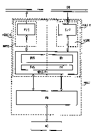
Figure 5 shows a block circuit diagram of the HDLC transmitter unit
HDLC-S. The data to be sent are inserted into a databus DB with this via the
parallel-
to-serial converter P/S. Whenever a data word has been output on the databus
DB, a
new data word is loaded into the parallel-to-serial converter P/S from the
data hold
register DHS. At the beginning of a new time slot, all data and states of the
HDLC
processor HDLC-P that were intermediately stored in the data hold register DHS
and
in the state parameter register SPS are exchanged by the HDLC processor HDLC-
P.
Figure 6 shows the HDLC receiver unit HDLC-E in detail. The critical
2 o elements of the HDLC receiver unit HDLC-E are thereby the serial-to-
parallel
converter S/P, the register data hold DH, a state parameter register SP, a
unit for byte
processing BV, a unit for frame processing FV as well as a frame buffer FB.
The data intermediately stored in the state parameter register SP for a
respective time slot are deposited in a state table ST of the byte processing
unit BV
2 5 after the current time slot. The state table ST is organized such in the
byte processing
unit BV that the data of a future time slot are loaded into the state
parameter register
SP every time given a time slot change. The data fetched from the data hold
register
DH are arranged in an event queue EQ, a link element between the byte
processing
unit BV and the frame processing unit FV, and are further-processed.
3 0 The data are read from the databus DB with the serial-to-parallel
converter
S/P of the first processing unit (WSPE). The data are deposited in the data
hold
CA 02338867 2001-O1-29
register DH. At the end of a length of a time slot that can be pre-set via a
counter, all
data and appertaining states are exchanged between the serial-to-parallel
converter S/P
and the state parameter register SP. The time slot width, the register content
and the
status thereof as well as further parameters are intermediately stored in the
state
5 parameter register SP. The state parameters that were read into the state
parameter
register SP are intermediately stored in the state table ST. The size of the
state table
ST corresponds to the maximum plurality of possible time slots of a
transmission link
in the synchronously operating data network SD. A beginning of a time slot
following a current time slot is calculated from the state data of the current
time slot.
The event queue EQ, which is arranged between the byte processing unit BV and
the
frame processing unit FV, is organized such that a prioritization
corresponding to the
transmission speed of a time slot or channel is possible. Among other things,
the data
of all HDLC channels are stored in the frame buffer FB following the frame
processing unit FV.
Figure 7 shows the HDLC transmitter unit HDLC-S. The data to be
transported in time slots or, respectively, channels are read from the frame
buffer FB
according to the arrow direction shown in the schematic drawing.
When data are read from the frame buffer FB or, respectively, from the
frame processing unit FVS in order to arrange these within a specific time
slot of the
2 0 PCM frame, the appertaining time slot numbers TS-Nr are assigned to the
data words
and are supplied via a data table DTS to a data hold register DHS in order to
be
intermediately stored there. Simultaneously with the intermediate storing of
the data
words to be inserted into the time slots of the PCM frames, the initialization
data STS
needed for the HDLC processor HDLC-P are stored [sic) from a state table of a
2 5 second memory unit STS arranged in the byte processing unit BVS by an
allocation
unit ZU in the second memory unit STS. Due to the initialization of the high
level
data link controller processor HDLC-P, the data words intermediately stored in
the
data hold register DHS are inserted into the time slots provided therefor in
conformity
with their purpose. At the end of a time slot, the part of the data word that
has not yet
3 0 been processed is transferred from the state parameter register SPS into
the second
memory unit STS together with the momentary status values of the high data
link
CA 02338867 2001-O1-29
6
control processor HDLC-P. Simultaneously during the transfer, the state
parameters
for the following time slot Tsn+x of the PCM frame proceed into the state
parameter
register SPS and the data words therefor proceed into the data hold register
DHS.
Corresponding to the pre-settings of the high level data link control
processor HDLC-
P, the data intermediately stored in the data hold register DHS are inserted
into the
time slots of the PCM frame. Given a renewed time slot change, the state
parameters
of the high level data link control processor HDLC-P as well as the data are
loaded
into the data hold register DHS or, respectively, the state parameters are
loaded into
the state parameter register SPS and are intermediately stored in the state
table STS.
New data and settings for the high level data link control processor HDLC-P
required
for the coming time slot are defined by the allocation unit ZU.
The data for the data table DTS are forwarded in the frame processing unit
FVS with the assistance of the event queue EQS. The data of all possible time
slots
are intermediately stored in the data table DTS in a transmission frame for
the data
hold register DHS. As a result thereof, it is possible to also implement a
frame
processing outside the time slot. A data processing corresponding to the
respective
transmission rate is possible with the assistance of the event queue EQS. The
time
slot numbers TS-numbers of the last, current and following time slot are
calculated in
the byte processing unit BVS from the position of the time slot and from the
time slot
2 o length in the transmission frame. The state parameters SPS of all time
slots to be
processed are stored in the state table STS. The size of the state table STS
always
corresponds to the maximally possible plurality of time slots. The state
parameters
that are entered in the state parameter register SPS contain the following
information:
time slot width, bit number in the data word as well as shift register content
and
2 5 further state information.