Note : Les descriptions sont présentées dans la langue officielle dans laquelle elles ont été soumises.
CA 02339943 2001-02-07
WO 08/08730 PCT/IlS99/17283
-1-
ELECTRO-OPTICAL SEMICONDUCTOR DEVICE WTfH A POLYIMIDE/SILICON OXIDE BI-LAYER
BENEATH A
METAL CONTACT LAYER
BACKGROUND OF TI-IE INVENTION
As device speed:. increase, parasitic capacitance increasingly becomes a
design
factor. This is especially true more recently in semiconductor electro-optical
devices.
As the optical qualities continue to be incrementally refined, parasitic
capacitances in
these already small devices become the criticality in the speed of operation.
In electro-optical devices, the metal contact layers and wire bond pads give
rise
to a large proportion of total device capacitance. For example, considering
the example
of ridge-waveguide arclutectures, ridge structures function as waveguides in
optically-
active epitaxial layers (e:pilayers) to produce lasers and modulators, or even
passive
waveguides. In most configurations, the ridge is etched into the epilayers,
and a wire
bond pad is constructed adjacent to the ridge. A p-metal contact layer, below
the pad,
conducts current between the pad and the top of the ridge structure so that
current is
injected down through the ridge and the underlying active layer to the
substrate.
Current is controlled to be injected only through the ridge by a
passivation/insulation
layer that is located bet,,veen the semiconductor and metal contact layer in
all places but
the ridge top. The current is injected to create light generation at the
active layer in the
case of a laser. It also can apply the reverse bias voltage to control the
absorption
properties in the case o1' a modulator. Other cases include an optical switch,
optical
detector, optical amplifier, or integrated waveguide device in which at least
two of the
mentioned devices are integrated. In these devices, the largest structures are
the bond
pads adjacent to the ridge, which are capacitively coupled to the typically
grounded
substrate of the device.
CA 02339943 2001-02-07
WO 00/08730 PCT/US99/17283
-2
In the past, silicon oxide, i.e., silicon dioxide, has been used under the
metal
contact layer and bond pad as the passivation layer and to facilitate
planarization, if
necessary. There are cer>:ain advantages associated with this material system.
Silicon
oxide deposition processes are well-known and integrated into existing
fabrication lines,
5 and it further adheres well to gallium arsenide- and silicon-based
substrates. Moreover,
good adhesion can be obtained between the metal contact layers and the silicon
oxide,
reducing the risk of wire pull-off after wire bonding processes to the wire:
bond pad.
Silicon oxide, however, has drawbacks that are related to the device's
electrical
properties. Silicon oxide's dielectric properties create intrinsic
limitations. Moreover,
capacitance is proportional to the size of conductors and inversely
proportional to the
distance between conductors. Assuming that the size of the bond pad ca~i not
be made
smaller due to the mechanics of wire bonding to the pad, the only way to
decrease
capacitance is to increase the distance between the contact layer and
substrate, but
stress-free silicon oxide layers of a micron or thicker are difficult to
produce. Thus, a
different material system is needed to further reduce capacitance.
Accordingly, some have replaced silicon oxide with polyimide passivation
layers. Polyimide has considerably more favorable dielectric properties, can
be
similarly integrated into the existing device fabrication production lines,
and has well
characterized performance in electronic devices through its ubiquitous use in
electronic
circuit boards. This has occurred because of polyimide's attractive bala~lce
of thermal,
mechanical, and electrical properties.
SUMMARY OF THE INVENTION
Experimentation has exposed a problem associated with the use of polyimide as
an insulation layer. Poor adhesion at the polyimide layer in semiconductor
systems can
raise performance issues in commercial-grade devices.
Adhesion of the polyimide to the semiconductor layer, such as a silicon oxide
coverage layer, can be controlled. Recent developments in adhesion promoters
CA 02339943 2001-02-07
WO 00/08730 PCTNS99/17283
-3
facilitate the chemical preparation of silicon oxide passivation layers, for
example, to
receive the polyimide.
The problems instead arise when the metal contact layers are deposited on the
polyimide. Good adhesion is required because wire bonding processes, such as
5 ultrasonic wire bonding, create substantial mechanical stress at the
polyimide/contact
layer junction. This can cause substantial failures at the time of wire
bonding or later
during deployment at the; junction. In most cases, such uncertainties are
unacceptable in
a commercial device.
The present invention is directed to an electro-optical device and method for
its
10 fabrication. The invention utilizes a polymeric dielectric layer, which
preferably
polyimide. Consequently, capacitance is minimized because of polyimides
favorable
dielectric properties and the thickness to which it can be deposited to
facilitate the high
speed operation of the device. According to the invention, however, a silicon
oxide
interlayer is used between the metal contact layer and the polyimide. This bi-
layer of
15 silicon oxide and polyirnide facilitates the ultimate adhesion between the
metal contact
layer and the underlying, device since good adhesion can be obtained between
the silicon
oxide layer and the polyimide layer with the invention and between the metal
layer and
silicon oxide layer.
Preferably, the polyimide is roughened to increase the surface area contact
20 between the polyimide layer and silicon oxide layer to further increase
adhesion and
thus the pull-off force required to separate the metal contact layer from the
device.
While such roughening can be achieved through plasma etching, in a preferred
embodiment, the polyimide layer is roughened by patterned etching.
Specifically, a
patterned photoresist is used as a etch-protection layer to form a series of
wells in the
25 polyimide layer. Preferably, the pitch between successive wells is I to 2 0
microns.
CA 02339943 2001-02-07
WO 00/08730 PCTNS99/17283
-4
This approach is also useful in reverse-ridge configurations where, with
conventional processes, it is additionally difficult to obtain good silicon
oxide coverage
underneath the ridge overhang and thus planarization.
The above and other features of the invention including various novel details
of
5 construction and combinations of parts, and other advantages, will now be
more
particularly described with reference to the accompanying drawings and pointed
out in
the claims. It will be understood that the particular method and device
embodying the
invention are shown by way of illustration and not as a limitation of the
invention. The
principles and features of this invention may be employed in various and
numerous
embodiments without departing from the scope of the invention.
BRIEF DESCRIPTION OF THE DRAWINGS
In the drawings, like reference characters refer to the same parts throughout
the
different views. The drawings are not necessarily to scale, emphasis instead
being
placed upon illustrating 'the principles of the invention. Of the drawings.
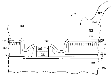
Fig. 1 is a cross-sectional view of an electro-optical ridge-waveguide
modulator
according to the present invention;
Fig. 2 is a top plan view of the electro-optical ridge-waveguide modulator
showing the extent of the metal contact layer and wire bond pads prior to chip
separation, according to the present invention;
Fig. 3 is a cross-sectional view of the inventive modulator during
fabrication,
before the ridge etch;
Fig. 4 is a cross-sectional view of the inventive modulator during
fabrication,
after the ridge etch;
Fig. 5 is a cross-sectional view of the modulator after the deposition of the
polyimide layer on the silicon oxide passivation layer;
Fig. 6 shows the etching of the extent of the polyimide layer;
Fig. 7 shows the developed photoresist layer for patterning the polyimide
layer;
Fig. 8 shows the: patterning etching of the polyimide layer;
CA 02339943 2001-02-07
WO 00/08730 PCTNS99I17283
-5
Fig. 9 shows the deposition of the silicon oxide interlayer and etched-back
photoresist layer, exposing the ridge structure;
Fig. 10 shows thf: formation of the p-metal contact layer and bond pad;
Fig. 11 is a top plan view of another embodiment of the inventive modulator in
which the extent of the metal contact layer is reduced to further decrease
capacitance;
Fig. 12 is a cross-sectional view showing the application of the present
invention to a reverse-ridge laser diode structure according to the invention;
Fig. 13 shows another embodiment in which two different semiconductor
electro-optical devices are integrated together, according to the present
invention; and
Fig. 14 is a graph showing the distribution of inventive devices as a function
of
pull force in grams required to separate the ultrasonically bonded wire.
DETAILED DESCRIP'1CION OF THE INVENTION
Fig. 1 is a cross-sectional view of a ridge-waveguide modulator 10, which has
been constructed according to the principles of the present invention.
15 The substrate material 100 is preferably indium phosphide InP. .An
epitaxial
InGaAsP layer 104, used as an etch stop layer during processing, covers the
substrate.
A preferably indium aluminum gallium arsenide InAIGaAs or indium gallium
arsenide
phosphide InGaAsP epitaxial active layer 110, which is confined within a ridge
112,
provides the electro-optical characteristics of the device. The active layer
110 is
bounded above and below by cladding layers 106, 108, which are preferably InP.
A silicon oxide passivation layer 114 is deposited on the etch stop layer 104
and
on the side walls of the ridge 112. In a preferred embodiment, the silicon
oxide
passivation layer can bf; relatively thin, 2000-5000 Angstroms (/~) thick,
since a
polyimide layer 116A,I3 is used for capacitance reduction through the
separation of p-
metal layer 122 from the usually grounded substrate 100. A silicon oxide
interlayer 118
is deposited on the polymeric dielectric layer 116, which is polyimide.
CA 02339943 2001-02-07
WO 00/08730 PCT/US99/17283
-6-
The polyimide layer 116A,B is roughened prior to the application of the
silicon
oxide interlayer 118. This is performed to increase the surface area of the
interface
between the interlayer 1 lu 8 and polyimide layer 116. While the roughening is
performed
through plasma etching, for example in some embodiments, in the preferred
5 embodiment, the surface area of the polyimide is increased by forming a
series of etched
wells 120 in the top surface of the polyimide layer 116. The pitch of these
wells, i.e.,
the distance between the centers of successive wells is preferably 1 to 20
microns. A
pitch of 8 microns is used in the preferred embodiment. The depth of the wells
is
approximately 0.3-2.0 microns, preferably 0.7 microns.
10 The p-metal contact layer 122 is deposited on the silicon oxide interlayer
118
with an ohmic contact to the top of ridge 112. In a preferred embodiment, the
contact
layer is a tri-metal of tit~~rzium, platinum, and gold . A large bond pad 124,
128 of gold
is then formed on the contact layer 122, adjacent to the ridge, to receive a
wire 126, with
a wire ball 126A formed; on the pad 124, preferably by ultrasonic wire
bonding. A ridge
15 injection current from wire 126 is conducted down through the ridge 112
through the
active layer 110 by the p-metal contact layer 122.
Fig. 2 is a top plan view showing three A, B, C ridge-waveguide modulators of
a
wafer prior to scribing/cleaving separation into individual devices. Each has
the ridge
112 and the metal contact layer 122 running the length of the ridge. The metal
contact
20 layer 122 also underlies the bond pad 124. Also shown are the square wells
120, which
have been formed in the: underlying polyimide layer 116 to facilitate the
adhesion of the
silicon oxide interlayer 118, covering all areas on the semiconductor except
the tops of
the ridges 112, and thus the adhesion of the metal bond pad 124 to the device.
Figs. 3 through 10 illustrate the process for manufacturing the inventive
ridge-
25 waveguide modulator 10.
As shown in Fib;. 3, a silicon oxide layer 122 is deposited over substrate 100
and
on epitaxial layers 104, 106, 108, 110. The preferred thickness of oxide layer
122 is
CA 02339943 2001-02-07
WO 00/08730 PCT/US99/17283
_'7_
2200A. A first photoresist layer 130 is deposited on the silicon oxide layer
122. Using
lithography processes, all of the first photoresist 130 is removed except for
that over
region 1 I2. Oxide layer 122 is then removed in a dry, plasma etch, except for
that
portion of the oxide layer 122 under the remaining photoresist. A wet etch is
then
performed down to InGaAsP etch stop layer 104. This process produces the ridge
structure 112 shown in Fig. 4.
in alternative emlbodiments, when diode lasers are being manufactured, the
etch
is typically not performed down to the depth of active layer 110.
Fig. 5 shows the deposition of the polyimide layer 116. Specifically, the
remainder of the oxide layer 122 is removed from the top of the ridge 112. A
silicon
oxide passivation layer 1.14 is then coated over the surface of the device
using
preferably chemical vapor disposition. The thickness of the passivation layer
114 is
approximately B=S,OUO A. Then, a thick polyimide layer, between 2 and 5
microns, is
spun on over the silicon oxide passivation layer 114. In the preferred
embodiment, the
thickness is C=2.5 microns. Other polymeric dielectric materials may be used;
the key
feature is the compatibility with the semiconductor manufacturing process.
The surface of'the passivation layer 114 is prepared prior to the polyimide
deposition using an adhesion promoter. Presently, DuPont's Pyralin~ brand
organosilane is being used.
20 A second photoresist layer 152 is then coated over the polyimide layer 116
to
facilitate its patterning. The second photoresist layer 152 in the region 154
surrounding
the ridge 112 is first removed by photolithography processes. The polyimide is
then
etched using oxygen plasma etching in the preferred embodiment.
As shown in Fig;. 6, after the photoresist layer 152 is completely removed,
portions of the polyimide layer 116A and 116B are left on either side of the
ridge 112.
CA 02339943 2001-02-07
WO 00/08730 PCT/IJS99/17283
_g_
The portion 116A of the polyimide layer 116A extends under the entire region
where
the bond pad is to be formed.
Fig. 7 shows the ateps associated with patterning the polyimide layer 116.
Specifically, a third photoresist layer is deposited and then etched in the
desired pattern
5 for the polyimide layer 116. In the preferred embodiment, a series of wells
120 are
formed at even spacings in the third photoresist layer 154. In the preferred
embodiment,
the thickness of the third photoresist layer 154 is approximately 1.5 microns.
Thus, the
photoresist layer is patterned in a grid, in the present embodiment.
As shown in Fig. 8, the photoresist layer 154 and polyimide layer 116 are
10 exposed to an oxygen plasma etch. This etch attacks both the remaining
portions of the
third photoresist 154 and exposed portions of the polyimide layer 116. There
is
approximately a 1:1 ratio in the etching efficiency of the photoresist
relative to the
polyimide. As a result, the wells 120 are etched into the polyimide layer 116A
while
the time of the etch is controlled such that the third photoresist 154 is not
entirely
15 removed from the top of the polyimide layer 116A. The oxygen plasma etch,
however,
does not attack the oxide: layer 112 protecting the ridge 120. The remaining
portions of
the portions of the third photoresist layer 154 are then removed and the
silicon oxide
interlayer 118 is deposited as shown in Fig. 9. The silicon oxide layer fills
into the
wells 120 in the polyimi.de layer 116A to increase the surface area adhesion
between the
20 silicon oxide interlayer 118 and polyimide layer 116A. The formed wells 120
in the
polyimide layer 116 increase the contact area between the polyimide and
silicon oxide
to provide a good net adhesion between the silicon oxide and polyimide of the
bilayer,
even though generally tl:re adhesion of silicon oxide on polyimide is poor.
As also shown in Fig. 9, a fourth, hard-baked, photoresist layer 156 and a
sixth,
25 soft-baked photoresist layer 157 are next deposited, and then using
lithography
processes is removed in the regions surrounding the ridge 112. This is
accomplished
using a photoresist pullback technique in which oxygen plasma etching is first
used
CA 02339943 2001-02-07
WO 00/08730 PCT/US99/17283
-9
followed by CHF3 to etch, the portions of oxide passivation layer 114 and
interlayer 118
on top of the ridge 112.
Finally, as shown in Fig. 10, the photoresist layers 156 and 157 are removed.
This exposes the ridge peak allowing the p-contact layer 122 to form an ohmic
contact
to the ridge. The gold bond pad 124, 128 is then formed on the polyimide pad
116A,
116B at both sides of the ridge 112..
Fig. 11 shows another embodiment of the present invention. This is a top view
of a device similar to that shown in Fig. 2. The area 140 of the contact layer
122
between the pad 124 and the ridge 112 has been reduced. This further reduces
parasitic
capacitance.
Another approach is simply to reduce the size of the bond pad 124. There are
limitations, however, in t:he minimum size for this bond pad due to the
alignment
accuracy of and wire ball size (126A) used in existing wire bonding
technology.
Fig. 12 is a cross-section of another embodiment of the present invention in
which similar features have been assigned the same reference numerals. This
architecture uses a reverse ridge structure 112 in which the ridge etch is not
performed
to the depth of active layer 110. An advantage associated with using the
polyimide
layer 116 in this configuration is the fact that it coats well in the regions
'under the ridge
overhangs 142 to provide planarization.
20 Fig. 13 shows another embodiment of the present invention. It integrates
two
different semiconductor electro-optical devices, both of which utilize the
present
invention to form wire bond pads 124 (shown in phantom) in order to reduce
parasitic
capacitance. One device 161 is preferably a laser with a ridge etch stopped
above the
active layer 110. The other device 162 is preferably an optical modulator, an
amplifier,
or a detector, which has the ridge 112 etched through the active layer 110, or
staying at
CA 02339943 2001-02-07
WO 00/08730 PCT,NS99/17283
-10
the same level as the laser 161. In both cases p-metal contact layer 122
connects the
pads 124 to the device ridge 112.
Fig. 14 is a graph showing the distribution of devices utilizing the invention
as a
function of pull force in grams, i.e., the amount of force required to
separate the wire
5 (126) from the device (10). As demonstrated, the devices sustained pull
forces of
greater that 7 grams with many devices sustaining pull forces of 11 grams or
higher.
This compares favorably with existing commercial and military specifications
requiring
pull forces of only greater than 3 grams.
While this invention has been particularly shown and described with references
10 to preferred embodiments thereof, it will be understood by those skilled in
the art that
various changes in form and details may be made therein without departing from
the
spirit and scope of the invention as defined by the appended claims. Those
skilled in
the art will recognize or be able to ascertain using no more than routine
experimentation, many equivalents to the specific embodiments of the invention
15 described specifically herein. Such equivalents are intended to be
encompassed in the
scope of the claims.