Note : Les descriptions sont présentées dans la langue officielle dans laquelle elles ont été soumises.
CA 02340312 2001-07-11
- 1 -
TIThE OF THE INVENTION
Electric Power system
BACKGROUND OF THE INVENTION
The present invention relates to an electric power
system.
A conventional battery protective circuit for
secondary batteries connected in series is disclosed in
Japanese laid-open Patent Publication Hei 8-78060.
Fig. 11 is a view showing the conventional battery
protective circuit. In Fig. 11, reference numerals 1101
indicate secondary batteries, 1102 voltage detection
circuits, 1103 resistors, 1104 comparators, and 1105 an
FET .
The two secondary batteries 1101 are connected in
series and the voltage detection circuits 1102 are
connected across the respective secondary batteries1101.
To each input of the comparators 1104, a reference voltage
divided by the voltage of the resistors 1103 connected in
series and the output of the voltage detection circuits
1102 are connected respectively.
Both outputs of the comparators 1104 are connected to
the gate of the FET 1105, inserted in series with the
secondary batteries 1101.
The voltage detection circuits 1102 detect the
s a
CA 02340312 2001-07-11
- 2 -
voltages of the secondary batteries 1101 respectively and
the comparators 1104 compare the detected value with the
reference voltage divided by the voltage of the resistors.
Tn~hen any of the secondary batteries 1101 is fully charged and
the detected value of any of the voltage detection circuits
1102 is more than the reference voltage, the output of any
of the comparators 1104 becomes low, the FET 1105 is
turned off, and charging is stopped.
The conventional battery protective circuit requires
the exclusive voltage detection circuits 1102
for the two secondary batteries 1101 connected in series..
The reason is that the potential levels of the detected
values of the voltage detection circuits 1102 are different
from each other on the basis of: the .lowest negative terminal
of the secondary batteries 1101.
The voltage divis~.on.resistors 1103 must be also
installed exclusively for the secondary batteries 1101.
The values of the resistors 1103 are always varied
from the nominal value within a certain range in the
production process so that the reference value for
specifying full charging is also varied and the precision
of the reference voltage is lowered.
Further, to make the different potential levels of
detected values of the voltage detection circuits 1102
Z
CA 02340312 2001-07-11
- 3 -
equal by level-shifting, the comparators 1104 rnus~ be
installed exclusively for the secondary batteries 1101.
Moreover, the withstand voltages of the
comparators 1104 must be equal to the total voltage of the
batteries connected in series.
Even if a circuit fulfills the same function for each
of the secondary batteries like this, a circuit fit to each
potential level is required for each of the secondary
batteries. Accordingly, assuming that a plurality of
batteries 1101 are additionally connected in series, the
number of circuits increases and the cost, size, and power
consumption also increase. Parts of the comparators 1104
having a withstand voltage meeting the total voltage of
the batteries connected in series do not actually exist
and it is difficult to realize this circuit.
Summary of the Invention
The electric power system of the present invention has
a plurality of capacitors connected in series, a plurality
of DC-AC conversion circuits for converting and outputting
each DC voltage of the plurality of capacitors to an AC
signal, having an AC component equivalent to the inter-
terminal DC voltage of each of the capacitors
superimposed on each DC voltage, a plurality of
condenser couplers for breaking each DC voltage from
CA 02340312 2001-07-11
- 4 -
each output of the plurality of AC-DC conversion circuits
and outputting the AC components respectively, and a
processing circuit for selecting each output of the
plurality of condenser couplers and detecting the
inter-terminal DC voltage of the corresponding capacitor
from the selected AC component.
The electric power system of the present invention has
a plurality of capacitors connected in series, a plurality
of DC-AC conversion circuits for converting and outputting
each DC voltage of the plurality of capacitors to an AC
signal having an AC component equivalent to the inter-
terminal DC voltage of each of the capacitors
superimposed on each DC voltage, a plurality of
condenser couplers for breaking each DC voltage from
each output of the plurality of DC-AC conversion circuits
and outputting the AC components respectively, a
processing circuit for selecting each output of the
plurality of condenser couplers, converting the selected
AC component to a digital signal, and detecting the
inter-terminal DC voltage of the corresponding capacitor
from the digital signal, wherein the processing circuit
has a selection circuit for selecting output from the
plurality of condenser couplers, an A-D conversion circuit
for converting the selected AC component to a digital
signal, and a microcomputer for detecting the inter-
CA 02340312 2001-07-11
terminal DC voltage of the corresponding capacitor from
the digital signal.
The present invention is an electric power system,
wherein the processing circuit has an AC-DC conversion
circuit for converting the AC component selected by the
selection circuit to a DC voltage that is full-wave
rectified and supplies the converted DC voltage to an
A-D conversion circuit.
The present invention is an electric power system,
wherein each circuit of at least a part of the DC-AC
conversion circuit, condenser coupler, and control
circuit is enclosed by an insulating trench formed on the
substrate.
Brief Description of the Drawings
Fig. 1 is a circuit diagram showing the first
embodiment of the electric power system of the present
invention;
Fig. 2 is a circuit diagram showing the second
embodiment of the present invention;
Figs. 3a and 3d are waveforms showing the operations
of Figs. 1 and 2;
Fig. 4 is a circuit diagram showing the third
embodiment of the present invention;
Fig. 5 is a circuit diagram showing the fourth
embodiment of the present invention;
Fig. 6 is a circuit diagram showing the fifth
embodiment of the present invention;
P F
CA 02340312 2001-07-11
- 6 -
Fig. 7 is a view showing a substrate an IC of the
sixth embodiment of the present invention;
Fig. 8 is a sectional view of Fig. 7;
Fig. 9 is a circuit diagram showing an seventh
embodiment of a sunlight power converter to which the
present invention is applied:
Fig. 10 is a circuit diagram showing an embodiment of
a part of an automobile to which the present invention is
applied:
Fig. 11 is a circuit diagram showing a conventional
battery protective circuit.
Description of the Preferred Embodiments
Embodiments of the invention are explained using
drawings in detail. Zike reference numerals designate
like parts throughout the drawings.
(Embodiment 1)
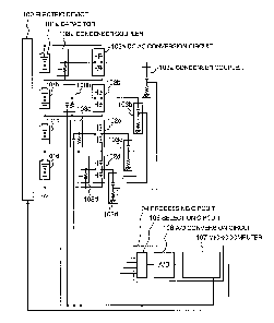
Fig. I is a circuit diagram showing the first
embodiment of the electric power system of the present
invention. In Fig. 1, reference numeral 100 indicates an
electric device, 101a, 101b, 101c, and 101d capacitors,
102a, 102b, 102c, and 102d DC-AC conversion circuits, 103a,
103b, 103c, and 103d condenser couplers, and 104 a
processing circuit. Reference numeral 105 indicates a
selection circuit, 106 an A-D conversion circuit, 107 a
microcomputer, and 108a, 108b, 108c, and 108d condenser
couplers.
In the present embodiment, the plurality of capacitors
E
CA 02340312 2001-07-11
101a, 101b, 101c, and 101d are connected in series and the
DC-AC conversion circuits 102a, 102b, 102c, and 102d are
respectively connected to the capacitors 101a, 101b, 101c,
and 101d in parallel. The DC-AC conversion circuits 102a,
102b, 102c, and 102d are respectively connected to the
selection circuit 105 of the processing circuit 104 via
the condenser couplers 103a, 103b, 103c, and 103d. The
selection circuit 105 is connected to the A-D conversion
circuit 106 and the A-D conversion circuit 106 is connected
to the microcomputer 107. A control signal output from
the microcomputer 107 controls the conversion operation
of the DC-AC conversion circuits 102a, 102b, 102c, and 102d
through the condenser couplers 108a, 108b, 108c, and 208d.
Also, the control signal is capable of arranging a
selection circuit to reduce the power consumption at the
output side of the microcomputer 107.
Both ends of the capacitors 101a, 101b, 101c, and 101d
connected in series are connected to the electric device
100 and transmit and receive power. The output of the
microcomputer 107 of the processing circuit 104 is
connected to the electric device 100 and transmits the DC
voltage condition of the capacitors 101a, 101b, 101c, and
101d to the electric device 100. Upon receipt of the DC
voltage condition information, the electric device 100
controls transmission and reception of power.
a
CA 02340312 2001-07-11
In this case, the electric device 100 is a second power
system (different power system , a motor system for an
elevator or an automobile, and a general electrical
apparatus.
The capacitors 101a, 101b, 101c, and 101d are an
electric energy storage device such as a nickel hydrogen
battery, a lead storage battery, a lithium secondary
battery, or an electric double layer capacitor or a
generating device such as a fuel battery.
The DC-AC conversion circuits 102a, 102b, 102c, and
102d are switches for alternately changing a.nd connecting
both ends of each of the capacitors 101a, 101b, 101c, and
101d to its output, and convert and output DC voltage of
the capacitors 101a, 101b, 101c, and lOld to an AC voltage.
The DC-AC conversion circuits 102a, 102b, 102c, and
102d are respectively composed of, for example, the
inverter circuit of P-MOS and N-MOS connected in series
shown in Fig. 1 and a control signal is supplied to both
gates of P-MOS and N-MOS which are input terminals from
the microcomputer 107 via the condenser couplers 108a, 108b,
108c, and 108d.
A control signal, for example, as shown in Fig. 3a,
is changed to an AC voltage having an AC component
superimposed on a DC voltage through the condenser couplers
108a, 108b, 108c, and 108d. The control signal is supplied
a P
CA 02340312 2001-07-11
- 9 -
to both gates of P-MOS and N-MOS, and P-MOS and N-MOS are
alternately turned on and off. For example, as shown
in Fig. 3b, the AC component is superimposed on the
inter-terminal DC voltage of each of the capacitors 101a,
101b, 101c, and lOld as output of the DC-AC conversion
circuits 102a, 102b, 102c, and 102d.
The condenser couplers 103a, 103b, 103c, and 103d are
respectively composed of a condenser and a resistance
connected in series and the common contact thereof is an
output terminal. In this case, each condenser breaks a DC
voltage and transmit the AC component and, for example,
transmits the output waveform to the inverter circuit as
shown in Fig. 3c.
The processing circuit 104 receives the output of the
DC-AC conversion circuits 102a, 102b, 102c, and 102d by
the selection circuit 105 and selects one output AC
component among them by a control signal from the
microcomputer 107. It may manually switch select the
output of the DC-AC conversion circuits.
One output AC component of the selection circuit 105
is converted to a digital signal by the A-D conversion
circuit 106, input to the microcomputer 107. The
microcomputer 107 detects the inter-terminal voltage of
the capacitors 101a, 101b, 101c, and 101d, infers the
charging condition, decides an error, decides voltage
CA 02340312 2001-07-11
- 10 -
unbalance between the capacitors , and monitor and manage
the capacitors.
Therefore, according to this embodiment, the DC-AC
conversion circuits 102a, 102b, and 102d can detect on
basis of the lowest negative terminal of the plurality of
capacitors lOla, lOlb, 101c, and lOld when the potential
level of each capacitor lOla, lOlb, lOlc and lOld is
different. The DC-AC conversion circuits 102a, 102b,
102c, and 102d functionally connected to the processing
circuit 104 via the condenser couplers 103a, 103b, 103c,
and 103d and a power unit for detecting the inter-
terminal voltage of each of the capacitors lOla, lOlb,
lOlc, and lOld. Thus, monitoring and managing the
condition of all capacitors can be realized.
Further, the. DC-AC conversion circuits 102a, 102b,
102c, and 102d are electrically insulated by the condenser
couplers 103a, 103b, 103c, and 103d and operate at the
voltage between the terminals of each capacitors i0la, 101b,
101c, and 101d. Therefore, the DC-AC conversion circuits
can be realized at a minimum withstand voltage to the
inter-terminal DC voltage of each of the capacitors.
Accordingly, it is possible to realize common use of
the processing circuit 104 including voltage detection for
the capacitors 101a, 101b, 101c, and lOld. This allows a
reduction in the number of circuits, the number of parts,
CA 02340312 2001-07-11
-11-
and power consumption, miniaturization, and cost.
(Embodiment 2)
Fig. 2 is a circuit diagram showing the second
embodiment of the power system of the present invention.
In Fig. 2, the difference from the first embodiment shown
in Fig. 1 is that an AC-DC conversion circuit 203 is newly
installed between the selection circuit 105 and the A-D
conversion circuit 106. The AC-DC conversion circuit 203
is composed of an inversion circuit 204, a switch 205, and
a CR filter 206.
The inversion circuit 204 inverts one output AC
component of the selection circuit 105 positive and
negative. The switch 205 selects the inverted value and
non-inverted value alternately and for example, as shown
in Fig. 3d, rectifies the full-wave. The CR filter 206
smoothes the oscillating component of the full-wave. In
this way, the AC-DC conversion circuit 203 restores one
output AC component of the condenser coupler 103 to a direct
current.
Therefore, according to this embodiment of the present
invention, a more precise inter-terminal voltage of the
capacitors 101a, 101b, 101c, and 101d can be detected.
(Embodiment 3)
Fig. 4 is a circuit diagram showing the third
embodiment of the electric~power system of the present
CA 02340312 2001-07-11
- 12 -
invention. In Fig. 4, reference numeral 401a indicates a
power circuit and 402a indicates a control power source.
The power circuit 401a is composed of a boot strap
circuit including the condenser coupler 108a and outputs
a voltage higher than the inter-terminal voltage of the
capacitor 101a.
In this case, the DC-AC conversion.circuit 102a is
composed of a multiplexes circuit and has the control power
source 402a. The control power source 402a is connected
to the power circuit 401a.
The input-output voltage of the multiplexes circuit
is generally lower than the voltage of the control power
source. When the control power source is changed, the
input-output characteristics (voltage transfer
characteristics such as rise time and breaking time) are
changed.
Meanwhile, the AC-DC conversion circuit 203 selects
the inverted value and non-inverted value of the condenser
coupler 103a alternately and rectifies the full-wave, so
that when the voltage transfer characteristics of the DC-AC
conversion circuit 102 are changed, an error is caused at
the time of conversion to a DC voltage.
Therefore, in this case, even when another power
circuit 401a is installed, and a voltage is supplied to
the control power source 402a, and the voltage of the
CA 02340312 2001-07-11
- 13 -
capacitor 101a is changed, the voltage transfer
characteristics of the DC-AC conversion circuit 102 are
kept unchanged. Therefore, the AC-DC conversion
operation of the AC-DC conversion circuit 203 is stabilized.
According to this, the DC-AC conversion circuit 102a can
convert the inter-terminal voltage information of the
capacitor 101a stably and precisely.
In Fig. 4, the power circuit 401a is composed of a boot
strap circuit. However, it may be composed of a switching
power source using an insulating transformer.
In Fig. 4, only the capacitor 101a is shown as a
representative. However, as shown in Figs. 1 and 2, the
capacitors are composed of four capacitors of 101a, 101b,
101c, and 101d connected in series, and the other
capacitors 101b, 101c, and 101d also have the same power
circuit and control power source as those shown in Fig.
4.
(Embodiment 4y
Fig. 5 is a circuit diagram showing the fourth
embodiment of the power unit of the present invention. In
Fig. 5, reference numeral 501a indicates a voltage control
voltage source and 502a indicates an AC-DC conversion
circuit power source.
The control circuit 104 includes the voltage control
voltage source 501a. In Fig. 5, the voltage control
CA 02340312 2001-07-11
- 14 -
voltage source 501a is shown as a switching power source
using an insulating transformer. However, it may be
realized by an insulating amplifier. The primary side at
one end is connected to the capacitor 101a. However, it
may be connected between both terminals of the train of
capacitors 101 connected in series.
The voltage control voltage source 501a outputs a
voltage corresponding to the inter-terminal voltage of the
capacitor 101a. The output thereof is supplied to the
AC-DC conversion circuit power source 502a of the AC-DC
conversion circuit 203.
The switch 205 of the AC-DC conversion circuit 203 is
composed of the same multiplexer as that of the DC-AC
conversion circuit 102a and the control power source
thereof is supplied from the voltage control voltage source
501a.
Here, the control power source 402 of the DC-AC
conversion circuit 102a is connected to the capacitor lOla.
Therefore, when the inter-terminal voltage of the
capacitor 101a is changed,~the voltage transfer
characteristics of the DC-AC conversion circuit 102a are
changed and the AC-DC conversion operation of the AC-DC
conversion circuit 203 is unstabilized.
A voltage cooperated to the power source of the DC-AC
conversion circuit 102a is also supplied to the AC-DC
CA 02340312 2001-07-11
- 15 -
conversion circuit 203 so as to make the voltage transfer
characteristics of the two coincide with each other,
thereby stabilization of the AC-DC conversion operation
is realized.
In the case, the power source in proportional to that
of the DC-AC conversion circuit 102a supplied to the
AC-DC conversion circuit 203, for example. Additionally,
it is possible to install the same number of the voltage
control voltage source as the number of the capacitor 101a
and arrange a sector between the AC-DC conversion circuit
power source 502a and a voltage control voltage source 501a
and arrange a sector between the output of microcomputer
107 and each condenser coupler 201a.
(Embodiment 5)
Fig. 6 is a circuit diagram showing the fifth
embodiment of the present invention. In Fig. 6, reference
numeral 602 indicates a storage circuit. The voltage
detection circuit 107 and the storage circuit 602 are
connected to the microcomputer 107.
The storage circuit 602 stores a voltage transfer error
and an error correction formula of the path from the DC-AC
conversion circuit 102a to the A-D conversion circuit 106
beforehand. The microcomputer 107 carries out correction
operations on the value of a digital signal of the A-D
conversion circuit 106 on the basis of the storage contents
CA 02340312 2001-07-11
- 16 -
of the storage circuit 602.
According to this, the inter-terminal voltage of the
capacitor 101a can be accurately detected and the
reliability of the electric power system can be improved.
The storage circuit 602 may be any of a mask ROM, EPROM,
flash memory and battery-back-up SRAM. It may be a separate
semiconductor chip other than the microcomputer 107 or may
be formed on a same semiconductor chip.
(Embodiment 6)
Fig. 7 is a view showing a substrate of a sixth
embodiment with the respective circuits of the first to
fifth embodiments of the electric power system of the
present invention being integrated. In Fig. 7, reference
numeral 701 indicates an SOI (silicon on insulator)
substrate, 702 an insulating trench, and 703 a bonding pad.
The insulating trench 702 is formed by filling a groove
formed inside the SOI substrate 701 with an insulator such
as Si02. The DC-AC conversion circuits 102a, the condenser
couplers 103a and 201a, and the control circuit 104
integrated on the same~SOI substrate 701 are enclosed by
the insulating trench 702.
According to this embodiment, each circuit can be
electrically insulated by the condenser coupler 103.
Therefore, each circuit can be low and withstand voltage and
the embodiment is suitable for the constitution to insulate
CA 02340312 2001-07-11
- 17 -
the circuits from each other by the insulating trench 702.
Fig. 8 is a sectional view indicated by an arrow A in
Fig. 7. In Fig. 8, reference numeral 801 indicates an
insulating layer, 802 a semiconductor layer, and 803 a
protective layer. The semiconductor layer 802 is divided
by a plurality of insulating trenches 702 and the area of
the DC-AC conversion circuit 102, the area of the condenser
couplers 103 and 201, and the area of the control circuit
104 are arranged from the left.
In this structure, the SOI substrate 701 having the
insulating layer 801 of Si02 with a width of about 2 microns
as an inner layer is prepared and each area is prepared
on it using the thin film process using a photomask.
The SOI substrate has a constitution that a multiple
insulating layer 801 of one layer of Si02 or additionally
a polysilicon layer having an oxidized surface overlaid
is overlaid on a single-crystal silicon substrate and
furthermore a single-crystal silicon semiconductor layer
is overlaid. Lamination uses a method for mirror-
polishing and overlaying the surface of a silicon oxide
film on the polysilicon surface and then bonding them by
heat-treating at a specific temperature.
The insulating trench 702 is formed by a method for
cutting a trench once and filling it with Si02 or
BPSG(Boro-Phospho Siicate Glass), a method for oxidizing
CA 02340312 2001-07-11
- 18 -
the trench wall thinly and filling the trench with
polysilicon, a method for coating polyimide resin or
SOG ( Spin-On Glass ) , or a method for irradiating oxygen ions
from the top and changing the semiconductor layer to an
insulating material.
The protective layer 803 is an insulator of Si02,
HZD(High Temperature how pressure ecomposition Films), or
SiN and includes a wiring layer of polysilicon or aluminum.
When folding the trench with 1.5 microms width and 15
microms depth and arranging in a square of about 160 microms,
this embodiment can obtain an insulating property of about
2 pF per a square of about 160 microns and a withstand
voltage of about 750 V per~one insulating trench 702 in
the DC withstand voltage test . When forming a pattern of
the insulating trench 702, to prevent an acute-angled
pattern, a circular arc pattern ( a radius of 2 to 5 microns )
as far as possible is used at a folding part or corner.
By doing this, the withstand voltage by electric field
concentration can be prevented from reduction.
In the embodiment, a plurality of circuits are
physically insulated from the SOI substrate 701 by the
insulating trench 702 and the insulating layer 801, so that
it is possible to directly bond the semiconductor chip to
the frame at the time of package mounting and dissipate
heat satisfactorily. Further, although an IC having a
CA 02340312 2001-07-11
- 19 -
multi-layer structure is warped a little, the thickness
of each layer can be adjusted by using an insulating
multi-layer, thereby an effect of dispersion of stress and
reducing in warp can be produced.
Here, assuming that the capacitors 101 are a module
battery that 10 nickel-hydrogen batteries are connected
to in series and the nominal electromotive voltage is 12 V,
the withstand voltage of DC-AC conversion circuit 102 is
set to about 18 V with a margin . The withstand voltage of
the control circuit 104 is about 5 V. The voltage when 25
module batteries mentioned above are connected in series
is 300 V, which is sufficiently lower than the insulating
property of the insulating trench 702. Therefore, the
condenser couplers 103 and 201 and the other circuits can
be integrated on the SOI substrate 701.
Since the aforementioned units can be integrated on
the SOI substrate 701, a reliable power unit which is
characterized in few parts, low cost, small size, low power
consumption, high control precision, and high noise margin
can be. realized.
(Embodiment 7)
Fig. 9 is a circuit diagram showing an seventh
embodiment of the present invention . In Fig . 9, reference
numeral 901 indicates a commercial power source, 902 a
sunlight generating set, 903 a load device, 904 a control
CA 02340312 2001-07-11
- 20 -
converter, and 905 a change-over device.
In Fig. 9, the electric power system is the same
structure as the embodiment 1 to 6. The plurality of
capacitors 101 are connected in series, and the DC-AC
conversion circuits 102 are respectively connected to
both ends of each of the capacitor 101. The output of
the DC-AC conversion circuits 102 is connected to the
selection circuit 105 of the control circuit 104, and AC-
DC conversion circuit 203, the voltage detection circuit
106, the microcomputer 107, and the storage circuit 602
via the condenser couplers 103.
The control converter 904 is connected to both ends
of the train of the capacitors 101. The microcomputer
601 in the control circuit 104 and the MCU in the control
converter 904 are connected.
Furthermore, the sunlight generating set 902, the load
device 903, and the control converter 904 are respectively
connected to the common commercial power source 901 via
the change-over device 905. At the same time, the sunlight
generating set 902, the load device 903, the control
converter 904, the change-over device 905, and the control
circuit 104 are connected via two-way communication.
The sunlight generating set 902 is a device for
converting the sunlight to DC power by a solar battery and
outputting AC power by an inverter device.
The load device 903 is a household electric appliance
CA 02340312 2001-07-11
- 21 -
such as an air conditioner, refrigerator, microwave oven,
or lighting fixture, an electrical appliance such as a
motor, elevator, computer, or medical appliance, or a
second power unit. The control converter 904 is a
charger-discharger for converting AC power to DC power or
converting DC power to AC power. It serves as a controller
for controlling charge and discharge and controlling the
sunlight generating set 902 and the load device 903
mentioned above.
Each of these devices may have the change-over device
905 in the own device. The power unit of the present
invention can be connected to the control converter 904
having a different constitution from that shown in the
drawing and the other devices.
According to this embodiment, when the power required
by the load device 903 cannot be supplied by the commercial
power source 901 or the sunlight generating set 902, power
is supplied from the capacitor 101 via the control
converter 904. When power supplyfrom the commercial power
source 9d1 or the sunlight generating set 902 is excessive,
unnecessary power is stored in the capacitor 101 via the
control converter 904.
During the aforementioned operation, when the
inter-terminal voltage of the capacitor 101 reaches the
discharge stop level or charge stop level, the control
CA 02340312 2001-07-11
- 22 -
circuit 104 transmits a signal indicating it to the control
converter 904 and the control converter 904 controls
charging or discharging.
In the aforementioned embodiments, the contract demand
and power consumption of the commercial power source 901
and the power generation rating of the sunlight generating
set 9f2 can be lowered and the equipment cost and running
cost can be reduced.
When power consumption is concentrated in a certain
time zone, the capacitor 101 supplies power to the
commercial power source 901 and when power consumption is
little, the power unit stores power, thus concentration
of the power consumption is moderated and the power
consumption can be averaged.
Furthermore, the control converter 904 monitors the
power consumption of the Load device 903 and controls the
load device 903, so that energy conservation and effective
utilization of power can be realized.
Fig. 10 is a circuit diagram showing an embodiment of
a part of an automobile to which an embodiment of the power
unit of the present invention is applied. In Fig. 10,
reference numeral 1001 indicates an alternator and 1002
indicates a DC load device . Fig . 10 is an extract of a part
of the constitution.
The alternator 1001 is connected to the train.of the
CA 02340312 2001-07-11
- 23 -
Capacitors lOla via the control converter 904.
The alternator 1001 executes engine start, assistance
of the.drive force (motoring), and power generation
(generation). During motoring, the train of the
capacitors 101 supplies power to the alternator 1001 via
the control converter 904. During generation, the
alternator 1001 inversely supplies power to the train of
the capacitors 101 via the control converter 904.
The DC load device 1002 is an electric load such as
a solenoid valve or audio unit or a second power unit such
as a lead battery. The DC load device 1002 is connected
to the train of the capacitors 101 via the change-over
device 905.
By doing this, an automobile for assisting the engine
torque at the time of departure and converting and storing
the kinetic energy to power at the time of application of
the break can be realized.