Note : Les descriptions sont présentées dans la langue officielle dans laquelle elles ont été soumises.
l a
CA 02341052 2001-03-15
ELECTR;O-OPTIC WAVEGUIDE DEVICES
BACKGROUND OF INVENTION
Field of Invention
The present invention relates, in general, to the design of optical waveguide
devices and specifically to the
design of the electrodes of such devices. The electrodes are intended to
change the characteristics of
electro-optic materials used for forming the planar channel-waveguides in
optical devices such as switches,
couplers, intensity madulators, phase shifters, and so forth.
Prior Art of the Invention
Optical switches and modulators made of electro-optic materials are the key
building blocks in the design
of high-speed optical communications networks. As migration continues to all-
optical devices utilizing a
large number of these building blocks within a single optical device or
circuit, their performance is
essential in achieving the design objectives in terms of a smaller overall
volume for a device or circuit,
Lower required voltage and power, less dissipated power, wider information
bandwidth and less inter-
channel cross-talk.
Electro-optic devices utilizing materials such as Lithium Niobate rely on the
controlled change of the
refraction index of the eiectro-optic material through applicatian of an
external electric f eld. The electric
field is set up by the application of a voltage source (constant voltage or
time varying signal) to a series of
electrodes (conductors) placed near the electro-optic material forming the
optical channel-waveguide(s).
The change in the refraction index results in changing the phase of the light
propagating in the optical
channel relative to a reference state (such as a component of the same light
propagating in a parallel
channel). Such relative changes can be productively utilized to design optical
switches, optical modulators
and optical phase shifters; just to natrxe a few.
1
l r
CA 02341052 2001-03-15
For a given level of desired relative phase shift, the efficiency with which
this external electric field is set
up controls the required voltage and the length of the optical channel and,
hence, the figure-of merit of
such optical devices in terms of the Voltage-Length product (V~ x L). This
efficiency is related to the
geometry and configuration of the electrodes relative to the light carrying
channels. For high-speed
applications, another important factor in the design of the electrodes is the
propagation speed of the
modulating (microwave) signal relative to the optical mode along the guiding-
channel(s). The differential
propagation speed will ultimately dictate the amount of information that can
be transmitted through the
channels (bandwidth). As a result, lm such applications, the design motivation
is not only to strive to
minimize Vet x L but also to ensure that the highest bandwidth is achieved.
Yet another factor controlling
the performance of the high-speed optical device is the attenuation of the
composite signal along the
optical channel(s). Such attenuation not only adversely affects the device's
insertion loss, the required
prime power and dissipated power, but also lowers the channel cutoff
frequency.
A more efficient electrode design will result in a lower Vet x L, which in
turn can be used productively to
reduce channel-length. This in turn reduces physical size, microwave and
optical losses, the required
prime power and dissipated power, aJnd increases the transmission bandwidth.
Alternatively, it can be used
to lower the voltage, which in turn reduces the required prime power and
dissipated power. Usually a
combination of these two options is exercised in a practical design tradeoff.
Electrode design for excitation of the electro-optic material has taken many
forms in the past two decades.
It started by using very thin surface-mount electrodes configured on either
side of the guiding channels or
located on top . To maximize the eiectro-optic effects, in the case of
channels made of LiNb03 as electro-
optic material, horizontal field excitation of the channel-waveguide is mostly
suited for x-cut crystals and
vertical field excitation is mostly suited for z-cut crystals.
The electric field generated by such a thin structure is fairly non-uniform
and highly localized around the
edges of the electrodes, with the magnitude of the field rapidly decaying as
one moves away from the
electrode edges. For a given voltage applied between an electrode pair (DC or
time varying voltage), field
intensity increases as the separation distance between the edges of the two
electrodes diminishes.
However, the field remains highly non-uniform and mostly concentrated in the
dielectric-air interface and
around the edges. As the edges of thc~ electrodes become closer, the electric
charges (fc~I a static field) or
electric currents (for time varying fields) interact, increasing conductor
losses and making impedance
2
i a
CA 02341052 2001-03-15
matching difficult (edge effects). Furthermore, for time-varying fields, the
cutoff frequency is relatively
low due to a combination of the skin-effect (higher conductance loss at higher
frequencies) and the
propagation speed differences along the guiding channels between the
modulating signal and the optical
mode.
For high-speed applications, single, double or multilayered thick electrode
designs have been proposed
(prior art) to reduce the skin-effect conductor losses and the differential
propagation speed as experienced
by the modulating signal. The favored configuration for this type of
arrangement is vertical field
excitation (principally vertical) by ph~cing the electrodes on top of the
guiding channels at the dielectric-air
interface plane. This type of arrangement still suffers from the defficiencies
resulting from non-uniform
excitation of the electro-optic materi~3 forming the guiding channels. More
importantly, as the guiding
channels possess a weak lateral confinement due to the small differential
refraction index existing between
the guiding channels and the surrounding dielectric medium, the electrode-
spacing (and as a consequence,
the spacing of the guiding channels) cannot be reduced to generate a larger
electric field for a given level
of applied voltage, since reduced spacing increases the optical coupling and
cross-talk between the guiding
channels. In all electrode configurations in the prior art, the electrodes are
always placed at the dielectric-
air interface. This is the case even fo:r the slightly-ridged waveguide, which
has the electrodes positioned
on top of the guiding channels.
~UPvIMARY OF THE INVENTION
Embodiments of the invention include devices for performing optical signal
switching, other optical
routing functions, and/or light inter ity modulation for high-speed external
modulator applications or in
optical phase-shifters while substantu~lly improving the figure-of merit of
such optical devices in terms of
reduction in the required Voltage-Length product (V~ x L). Preferred
applications include optical
switches, couplers, intensity modulators and phase shifters based on Lithium
Niobate Oxide (LiNb03),
although the present invention is applicable to any optical device requiring
efficient application of external
voltage to setup an electric field for changing the electro-optic
characteristics (index of refraction) of
optical waveguide channels and branches.
3O
In the present invention, the externally induced electric field is set up via
a plurality of electrodes, which
are strategically embedded, with. appropriate shape/thickness and penetration
level depending upon design
3
l a
CA 02341052 2001-03-15
or complete straddling of the channel(s); as opposed to surface-mount
electrodes of the prior art, which
rely on penetration of the external electric field in the crystal or
dielectric material. This enhanced
proximity, for a given level of applied voltage, allows the excitation of much
stronger electric field in the
vicinity of the light carrying wavegui<le channel(s). Furthermore, this
stronger field is, to a large extent,
spatially uniform over the waveguide channel(s), resulting in an overall
larger effective change in the
refractive index experienced by the optical fields. Such embedded electrode
geometry, if desired, can be
used to advantage toward substantially reducing the inter-channel coupling
(cross-talk) for a given level of
inter-channel spacing where such isolation is required for device performance
or reduction of inter-channel
spacing to reduce the overall size of the optical device, which may use a
multitude of optical switches
andlor modulators.
The improved physical confinement of the optical waveguide channels and
branches by the embedded
electrodes will make it possible to significantly reduce the possibility of
light attenuation and escape at
channel discontinuities and curved sections. Consequently, the required
channel discontinuities and
cuaved sections called for by the design of an optical device can be
configured with larger angles and
smaller radii of curvature to reduce the overall size of the optical device.
Furthermore, the proximity
configuration and the resulting efficiency of the embedded electrodes
facilitate impedance and phase
matching in a traveling-wave electrode configuration for external optical
modulators. This in turn permits
higher modulation speeds.
Accordingly, the present invention provides a novel design of electrodes and
methods of excitation of the
electro-optic material. Vertical field .configurations can be assumed by one
electrode placed on top of the
guiding channel at the dielectric-air interface and one embedded in the
dielectric below the channel.
However, for ease of manufacturing and also in order not to preclude the
option for partial confinment of
the channel, the electrodes are most convenient to be placed in a horizontal
field arrangement.
According to the present invention, after formation of the guiding channels)
in the dielectric by known
manufacturing methods (for instance in-diffusion or annealed proton exchange
APE for LiNb03,
rib/ridged waveguides or other methods of creation of buried waveguides), the
surface of the
crystal/dielectric is etched with the desired pattern for width, length and
penetration depth of the electrodes
by known techniques (for LiNb43, for instance, dry-etching using electron
cyclotron resonance etching or
wet etching or ion milling techniques). The electrodes (for instance, the
signal electrode in the center and
the ground electrades on the sides for a push-pull arrangement) are then
deposited as a single or multi~
4
l a
CA 02341052 2001-03-15
layered configuration using known manufacturing techniques. A thin layer of
optically transparent
insulating material (buffer layer} such as Si02 can be placed on the surface
of the etched dielectric before
deposition of a set of single or mufti-:layered electrodes towards controlling
conductor losses and
conductor/optical mode interaction and thermal and DC bias stability.
Furthermore, a thin adhesion layer
for electrods such as Ti can be deposited before placement of the electrods.
The electric field so set up is
highly uniform around the guiding channels}. As the optical channels are now
well isolated from each
other, the separation distance of the signal and ground electrodes is no
longer dictated by the inter-channel
isolation considerations of the guiding channels and the channels can now be
placed closer to each other.
The electrode separation distance for a guiding channel may now be decided
based upon the design
considerations for electric field inten<.~ity, impedance matching and other
design tradeoff parameters rather
than optical coupling considerations.
BRIEF DESCRIPTION OF THE DRAWINGS
The Preferred embodiments of the present invention will now be described in
detail in conjunction with the
annexed drawings, in which:
Figure la illustrates field excitation of waveguides with surface-mounted thin
electrodes, electric field
being prior art horizontal over the channel-waveguides;
Figure lb illustrates field excitation of waveguides with surface-mounted thin
electrodes, electric field
being prior art vertical over the channel-waveguides;
Figure 1e illustrates field excitation ofwaveguides with surface-mounted thick
electrodes, electric field
being prior art horizontal over the chmnel-waveguides;
Figure ld illustrates field excitation of slightly-ridged waveguides with
surface-mounted thick electrodes,
electric field being prior art vertical over the channel-waveguides;
Figure le illustrates field excitation of slightly-ridged waveguides with
surface-mounted rnulti-layered
thick electrodes, electric field being prior art vertical over the channel-
waveguides;
5
i v
CA 02341052 2001-03-15
Figure if illustrates field excitation of slightly-ridged waveguides with
surface-mounted mufti-layered
thick electrodes, electric field being prior art vertical over the channel-
waveguides;
Figure 2 illustrates the electrode design of the present invention embracing
the channel-waveguides on the
two sides, the electric field being horizontal across the channel-waveguides;
Figure 3 illustrates the electrode design of the present invention embracing
the channel-waveguides and
the buffer layer on the two sides, the electric field being horizontal across
the channel-waveguides;
Figure 4 illustrates the electrode design of the present invention embracing
the channel-waveguides and
the buffer layer on the two sides, with the electrodes partially protruding
above the dielectric-air interface,
the electric field being horizontal over the channel-waveguides;
Figure ~ illustrates the electrode design of the present invention embracing
the channel-waveguides and
the buffer layer on the two sides, with tapered electrodes partially
protruding above the dielectric-air
interface, the electric field being principally horizontal over the channel-
waveguides;
Figure 6 illustrates an application of the present invention to provide an
optical intensity modulator; and
Figure 7 illustrates an application of the present invention to provide an
optical switch.
DETAILED DESCRIPTION OF TIIE PREFERRED EMBODIMENTS
Figures 1 a to 1 d illustrate the electrode designs of the prior art. In these
figures, the channel waveguides
are represented by ellipses located within the dielectric region but in close
proximity with the dielectric-air
interface. The electrode configuration in these figures is co-planar symmetric
(Figure la) an asymmetric
(Figures Ib to lfj microstrip design. The electrodes (thin layers in Figures
is and lb, and thick layers in
Figures 1 c and 1 d) are placed at the air-dielectric interface surface on the
dielectric substrate. The external
6
l a
CA 02341052 2001-03-15
electric field set up by the application of a constant (DC) or time-varying
voltage across the electrodes
possesses a non-uniform spatial characteristic in terms of magnitude (maximum
field for time varying
case) and direction. As schematically represented by arrows, the electric
field so set up is principally
vertical under the electrodes and away from the edges (normal to the electrode
surface). As one
approaches the dielectric-air interface within the two edges of the adJacent
electrodes, the electric field is
principally horizontal.
Figure 1 a represents a configuration that places the channel-waveguides,
relative to the electrodes, in a
fashion that are excited principally by horizontally directed electric field.
Figure 1b represents a
configuration that the channel waveguides are excited principally by
vertically directed electric field.
Figure lc is the same as Figure 1b but with thicker electrodes. Figure 1d is
similar to Figure lc but the
channel waveguides are slightly ridged. Figure 1 a shows a mufti-layered
structure for the electrodes and
Figure 1 f depicts a configuration with a slight taper angle in the vertical
direction.
In all of the electrode configurations iin the prior art (Figures 1 a to 1 f),
the electrodes are always placed at
the dielectric-air interface. This is also the case for the slightly-ridged
waveguide, which has the
electrodes positioned on top of the guiding channels.
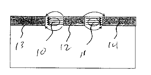
Figures 2-7 illustrate some of the embodiments and applications of this
invention. Figure 2 depicts an
embedded thick electrode structure in; the crystal/dielectric material on
either side of the channel-
waveguides. As shown, there are two channel-waveguides 10 and 11 with one
embedded electrode 12 in
between and two outer electrodes 13 and 14. The external electric field so set
up is highly uniform in
terms of its spatial distribution and polarization. The channel-waveguides
experience a strong uniform and
horizontally directed field. Figure 3 illustrates a similar configuration but
with a thin layer 15 of insulating
material (buffer layer) such as Si42 sandwitched between the surface of the
etched dielectric and the
electrodes for the purpose of reducing conductor .losses and controlling
conductor/optical mode interaction
and thermal and DC bias stabilization of the substrate material.
Figure 4 is a variation of the structure; in Figure 3. Here the electrodes 12,
13 and 14 protrude above the
dielectric-air interface in the direction of the latter. Such protrusion can
be beneficial in optimizing certain
design parameters given a defined level of device performance. Figure 5 is a
variation of the Figure 4
structure. In this geometry, the electrodes 12, 13, and 14 possess a small
angular taper in the vertical
7
i ~
CA 02341052 2001-03-15
direction to yet offer further flexibility in the design and optimization of
the overall device performance.
The fundamental character of the configurations presented by Figures 2-5 is
that the waveguide chatmels
are completeley embraced by the par dally or fully embedded electrodes, hence
experiencing a strong and
spatially uniform external field with prinicipally pure electric field
polarization. A further variation of
these configurations is the partial confinement of the channel waveguide if
certain levels of coupling
between the channels are mandated b;y the specific design at hand. The level
of interchannel isolation
(cross-talk) depends on the level of penetration of the electrodes and the
separation distance of the guiding
channels.
Figure 6 depicts an isometric view of an application of this invention in
devising an optical external
modulator. The channel-waveguides la and 1 Land the eiectrudes I2, I3 and 14
are embedded in the
crystal/dielectric substrate. The light entering from the input y junction is
split in two equal parts
(symmetric y junction). For a coplanar symmetric electrode arrangement such as
Figure 6, if a push-pull
excitation strategy is adopted, the center electrode is hot-electrode and the
two side electrodes will be
connected to each other and used as common (or reference) electrodes. The
voltage source will be
connected between the hot electrode and the common electrodes. This
arrangement will set up an external
electric field, which possesses opposite polarization in the two parallel
channel waveguides {see Figure 3
which depicts an x-z plane cut of Figvure 6 half way through the structure).
The change in the refraction
index, and hence the phase of the optical wave, is a function of the peak
magnitude of the applied voltage,
the separation distance of the hot versus common electrodes, the length of the
electrodes in the y direction
(active region) and the spatial unifornnity of the field in the guiding
channels. The higher the magnitude
and spatial uniformity of the electric field and the longer active region, the
larger is the relative phase
difference experienced by the two components of the light passing through the
channel waveguides. In the
absence of externally applied field, the two components of the optical wave
will add coherently in the
output y junction. If the active region is selected in such a way that, for a
given level of externally applied
voltage, the differential phase is 180 degrees, the coherent addition of the
two components of the optical
wave arriving at the output y junction would result in creation of a second-
order optical mode that cannot
be supported by the single-mode output y junction. Hence, light is radiated
into the substrate and the
transmitted light is minimum. For a t me varying external voltage source, this
results in intensity
modulation of the input light at the output port.
Figure 7 depicts an isometric view of an application of this invention in
devising an optical switch. The
channel-waveguides IO and I I and the electrodes 12, I3 and 14 are embedded in
the crystal/dielectric
8
l a
CA 02341052 2001-03-15
substrate. The light entering from input port 1, is split into two equal parts
at the input 3dB coupler. The
two components travel along the parallel waveguide channels. In the absence of
any externally applied
electric field, the light components combine back through the ouput 3-dB
coupler, resulting in maximum
light in output port minimum light in output port 1. With an external field
and for 180 degrees relative
phase shift between the channel-waveguides, the light completely swiches over
from line 1 to line 2.
The effectiveness of the electrode configuration of the present invention in
terms of a high degree of
spatial uniformity of the external electric field, guiding channel isolation
and larger field magnitude, the
length of the active region can be reduced substantially (to one half and
more) for a given level of
externally applied voltage. Alternatively, for the same length for the active
region, the voltage can be
reduced by the same factor.
The resulting savings in channel lengi:h has the added advantage that now the
aggregate deleterious effects
of a mismatch between the traveling-wave microwave modulating signal and the
optical wave in a high-
speed optical modulator is less pronounced. For the same reason, the
conductance losses of the electrodes
and dielectric losses of the substrate acre smaller. This results in a higher
cutoff frequency for the
modulating signal in an optical switch or intensity modulator and lower
attenuation for lower speed
applications.
In the design of optical y-junctions and 3-dB couplers in the prior art, the
branches of the y junctions or 3-
dB couplers generally have a very slow flare angle. 'This is in order to
ensure that the optical wave passing
through will not experience a sudden discontinuity, which is generally
accompanied by severe optical
mode attenuation and escape. In most applications, these branches have to be
connected to two parallel
guiding channels (such as interferornetric modulators considered here as
examples), which by themselves
will have to be largely separated to control inter-channel cross-talk caused
by evanescent mode coupling.
In the prior art designs, the branches of the small flare y junctions and 3-dB
couplers would have to be
inconveniently long to make such mating possible.
In the present invention, the embedded electrodes already isolate the optical
channel-waveguides. By
extending the hot and common electrodes in the proximity of input and output y-
juncrions and the 3-dB
couplers, the coupling between the branches can also be controlled. This
design flexibility can be
productively used in two ways. If a smaller physical size in the lateral
direction is desired, the branches of
9
i a
CA 02341052 2001-03-15
y junctions and 3-d8 couplers can asscume a very gradual flaring angle. But
now, the length of the
branches can be significantly reduced relative to prior art as the parallel
channel-waveguides may now be
positioned much closer to each other :due to the isolation offered by the
embedded electrodes. The
reduction in lateral dimension, coupled with a much shorter active region
required for a given level of
differential phase, substantially reduces the physical size of the optical
intensity modulator or switch. This
volumetric saving is a key performance parameter in the design of optical
devices, which integrate a large
number of switches and/or modulators.
Alternatively, for optical devices for which the longitudinal dimension is a
design driver, the branches of
the y junctions and 3-dB couplers can assume a relatively large flare angle
with less concern for light
attenuation and escape at such rapid transitions. This substantially reduces
the lateral size of the y-
junctions or 3-dB couplers. For large- cross-co~ect optical integrated
circuits utilizing cascaded switches,
such savings are benef cial.
For optical devices and integrated circuits for which low voltage, power
dissipation and/or power
consumption are the key performance: parameters (such as dense optical
integrated circuits), the electrode
design provided by this invention ma,y be beneficially used to substantially
reduce the level of the external
voltage source, the dissipated power ;end the required prime power.
to