Note : Les descriptions sont présentées dans la langue officielle dans laquelle elles ont été soumises.
CA 02341102 2001-02-19
WO 00/11677 PCT/US99/18894
Electrically Erasable Nonyolatile Memory
Background
This invention relates generally to nonvolatile memories and particularly to
electrically erasable nonvolatile memories.
Nonvolatile memory cells are advantageous siaco they retain recorded
information
even when the powrer to the memory is turned off: There are several different
types of
nonvolatile memories including erasable programmable road only memories
(EPROMs),
elec'aicslly erasable and proble read only memories (EEPROMs) and flash EPROM
memories, EPROMs are erasable through light exposure but are electrically
programmable
by chattnei hot electron injection onto a floating gate. Conventional P.EPROMs
have the
l0 same programming functionality, but instead of being light erasable they
can be erased and
programmed by electron tunneling. Thus, information may be stored in these
memories,
retained when the power is off, and the memories rosy be erased for
reprogramming, as
necessary, using appropriate techniques. Flash B>;PROMs may be block era$ed,
typically
giving them better read access times than regular EEPROMs.
Curzet'ttly, flash memories have gained cot~sidarable popularity. For example,
flash
memories are often utilized to provide on-chip memory for micmcontarollcrs,
modem and
SMART cards and the like where it is desirable to store codes that may need
fast updating.
While flash memories and EEpROMr ere closely related, is many instances flash
memories arse preferred because their smaller cell size means that they can be
made more
eeenomica~lly. However, flash memories and BEPROMs often have very similar
cell
attributes.
When BEPROMs era erased, orie or.more of cells are erased in one operation, A
high
positive potential is applied to tire cell eotuces andlor drain while the
control electrode and
the substzste are grounded. As a result, negative charges on the floating gate
are drawn to the
source andlor drain region by Fowlez Nordheim turuseling. This techniaue is
cH'ectivc urhere
the dielectric between the floating gate olecGrode and the source and/or dress
regions ie very
thin.
A number of disadvantages arise from the conventions) Gracing t~htlique,
including
the fact that it creates the possibility of a reverse voltage breakdown
between the source
nndlor drain and substrate juncticms which would cause hot hole trapping in
oxide and
CA 02341102 2001-02-19
WO 00/11677 PCTNS99/18894
-2-
reliability problems. Chi Chang, et al. "Drain Avalanche and lkiole Trapping
Induced Gate
Leakage in Thin Oxide MOS Devices," IHEE Electron Device Letters, Vol. 9,
1988, pp. 58:3-
90. To overcome this, some designers have used a so-called double difi''used
junction to
enhance the junction avbetrate breakdown voltage. However, the doubly diffused
junction
has certain disadvantages, including (1) the fact chat it may require
additional cell size,
reducing the potential cell density and (2) it still has Gate Induced Drain
Leakage (GIRL)
current. Another potential solution is the use of relatively high negative
poteptials on the
control gate and bents less voltage is applied to the source. Sameer S. Haddad
et ai. TJ.S.
patent No. 5,077,691 titled, "Flash EBPROM Atray with Negative Gate Voltage
Erase
Operation.° This in turn would reduce the field across the source to
substrata junction.
However, as channel lengths become small this hole trapping becomes channel
length
dependent. This effect has been described as a possible "fundamental
limitation to the
scalisag of flash memory cells". :flan Chen, et al., "Short Channel hrttreaced
Degradation
During Diacltarge of Flash EEPlIOM Memory Cell", iFpM 1995 - 331, 13.6.1-
13.6.4. That
article indicates that during the discharge stress, the holes generated from
hand-to-band
tunneling travel through the silicon-to-silicon dioxide interface, ere
accelerated by the strong
lateral electric Geld, and gain au~cient energy to become energetic hot holes.
The actiele
explains that a negative gate voltage pulls these energetic hot holes to the
gate causing thorn
to bombard the surface, get trapped and create interface states. As channel
length decreases,
the lateral field increases, exacerbating the effect.
The article suggcats that the problem may be avoided by iacceasing the ehaanel
ledgth. Since this solution is counter to the longstanding industry fiend of
scaling devices to
increasingly smaller and smaller sizes neaulting in lower cost products is
smaller dimensions,
this solution is not particularly desirable. Chan, et al. auggesta that mother
solution to the
;Z5 problem is to apply a paeitive bias to the drain while discharging the
cell from the source
node. While the results diACUSaod in the arflicle indicate that this does
improve the ptablem to
a certain degree, some of the degradation appears to remain, even what this
approach is used.
It hoe also been suggested that using channel erase with a large negative
voltage
applied to the control gate and g voltage of five volka applied to a P-well
and an N-well could
3i0 improve gate distutb tolmaneo and reliability due to the decrease in hot
hole generation near
the soun:e region. See, T. ,linbo, et al., "A S-V-Only 16-Mb Flash Memory with
Sector Era9e
Mode", 1992 IEEE Jounn8l of Solid-State Circuits, Vol. 27, No. 11, November
1992 at pages
CA 02341102 2001-02-19
WO 00/11677 PCT/US99/18894
-3-
1547-1554. This requires a negative gate voltage that is about 113 higher than
that in the
drain erasure situation (the Haddad, et al. Patent 5,077,691). See, Hsing jen
Wan, et at.,
"Suppressi:ag Flash EEPROM Erase Leakage with Negative Gate Hiss and LDD
firase
Junction," Proc. ofIE~E VLSI Technology Symposium (lapan) May 1993, p. 81-2.
The inventor of the present invention believes that none of these approaches
is fuhy
satisfactory sad that there is a continuing need for an ef~iciant, scalable
erase mechanism.
Thus, while those skilled in this art have appreciated a number of advantages
that could
accrue from the use of a negative control gate potential in conne~tian with
EEPROM erase
cycles, a variety of defieiepcies have discouraged those of skill in this art
fmm pursuing those
'l0 advantages.
In accordance with one aspect of the present invention, a nonvolatile memory
cell is
formed in a P-type region. The memory cell also includes a transistor having a
floating gate
'.15 acrd a cont:ol gate and a pair of doped regions acting as a source and a
drain formed in the P-
typo region. The floating gate is erasable by tunneling of electrons from the
floating gate to
one of the doped regions. The P-type region and one of the doped repons are
biased
separately by positive potonEials. The difforonee between the doped region
bias and the P-
type mgion potential is less than Wcc and greater than zero. The control gate
is negatively
;t0 biased.
In accordance with yet anafher aspect of the present invention, 4 method for
easing a
metaory cell having a conhol gale, a floating gate, a channel, and a pair of
dpped regions
acting ss a source sad drain fanned in a P-well iri turn formed in an N-wall,
includes the step
of negatively biasing the control l;ate. The P-well arid one of the doped
regions are p~itivoly
;t5 biased ouch that the doped region biee minus the P-well bias is Less than
Vcc a»d more than
zero.
Beef Desctip 'ott Of The Drawing
Figure 1 is a schematic depiction of a ceh configuration far one embodiment;
and
Figure 2 ie a~schamatic depiction of s cell configuration for another
embodiment.
CA 02341102 2001-02-19
WO 00/11677 PCT/US99/18894
-4-
Detailed De~criptiotr
Referring to the drawing v~herein like reference charactets are used for like
parts
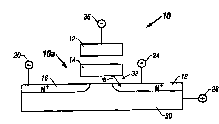
throughout the several views, a memory cell 10. shown in Fig. 1, includes a
control gate 12
and a floating gate t4. This structure is advasstageously implemented on a
semiconductor
layer 30 having situated thereon an electrically isolated floating gate 14.
However, the
particular cell structure ie not critical and the present invention could be
implemented using a
variety of memory cell structures, including, far example, split gate and
stacked gate cell
structures.
The substrate 30, which may be a p-type semiconductor, includes a heavily
doped
source region lb and a heavily doped dram region 18. The regions 16 and 18
could also
include lightly doped drain (LDD;! extensions (not shown). The drain bias
potential 24, the
substrate bias potential 26, the source potential 20 and gate bias potential
36 may be teiloted
to maximize the porfonmaace of the Boll.
The cell 10 may be road and pro~amlned using any known technique. The bias
potentials illustrated in Figure 1 ana for implementing a Fowiec Nardheim
tunneling of
electrons from the flaatirtg gate 14 primarily to the drain 18, as indicatotl
by the arrow "e".
During era~uro, the control gate 12 is foreod to a negative voltage of from -7
to -t4
volts, with the source bias potential 20 equal to or greater than the P~well
potential, By
keeping the coatral gate bias ruore positive than -11 volts, the process for
forming the cell can
2,0 be reads more compatible with standard logic pmceASes. By making the
source 20 potential
equal to or greater than the P-well potential the lateral electric field is
reduced, reducing band
to band tunneling induced hole trapping. Advents-geously, the source bier
potential is
between tire P-well sad drain bias potentials. Alternatively, the source may
float.
As for the drain difFution '18, and the substrate 30, they are biased to a
positive
2.5 potential close to Vcc or higher. Vcc i~ determitrod by the particular
technology utilized. For
example, it could be 5.0 to 1.8 volts with present technologies. This reduce
the electric field
acmse the juncti4a betweart the N+ diffusion 1 B sad the vubstrate 30. The
reduced GIRL
currcttt and the lateral electric held prevents acceleration of hot bolt
trsppiutg in the gate
oxide under the floating gate 14.
3.0 The dress 18 is preferably not biased to a voltage hfgher than the
substrate 30 to each
an oxunt th$t gate induced drain leakage (GIRL) becomes a problem. With
current
tcchnalogies, this means that the chair 18 bias i: advantageously not higher
than the substrate
CA 02341102 2001-02-19
WO 00/11677 PCT/US99/18894
-5-
30 bias by more than about one to two jolts. See S. Parks, at al., "Design for
Suppression of
Gate-induced Drain Leakage in hDD MOSFETs using a Quasi-two-dimensional
Analytical
Model; ' IEEE Transactions on Electron Devices, vol. 39, p. 1694-1703, 1992,
hereby
expressly incorporated by reference herein. In addition, if the drain 18 bias
aigni6cantly
S exceeds the substrate 30 bias, hot hole trapping may occur due to the
lateral junction field
acceleration. 1n general, it ie preferred that the drain IB bias minus the
substrate 30 bias be
greater than zero and less than Vc:c.
The ability to apply a positive voltage to tho substrate 30 is facilitated by
using a P-
well 30 embedded in sn N-well 32, as shown in Figure 2. The P-well voltage 26
is preferably
'l0 equal to or lea' than 1~1-well potential 28 to avoid P-weh/N-well forward
biasing. Thus,
applying a positive voltage of Vcc ar higher to the P-well 30, N-well 32 attd
the drain 18 can
eliminate hot hole trapping induced by GIRL while allowing the drain 1B
voltage to be raised
to Vcc or higher. Preferably, the drain bias minus the P-well bias is greater
than taro and lees
than Vce 4r at least greater than zero and equal to or less that Vcc.
15 The voltago across the capacitor 33 is the difference belwoen the floating
gate 1~
potential on the ~e hand and the difl-usion 18 and P-well 30 potentials, When
the differenec
exceeds B to 10 volts,'aufficient tunneling current is generated and the
floating gate 14 can be
erased w a negative potential in the time frame of a few milliseconds to a few
seconds,
depepding on the tunneling oxide 42 thickness.
:!0 Electrons tunnel to the drain region 1 B (drain era~te), The htnnelittg
current depande an
the voltage from the !loafing gate l4 to the drain 1 >;. However, by biasing
tho eoutee 16 in
the fashion illustrated for the drain 18, a source erase mechanism may be
provided instead of
the drain orsee moehanism. During source erase, the drain potential would be
controlled in
the same feahion as the sourcepotential in the drain eteae case.
:!5 The calls 10 and l0a may be funned using conventional piss technologies
such ae
a double poly, single metal CMOS process. The illustrative pararnotets set
fa!tth herein
contemplate a .35pm or lower feature size with Vcc potontiala of 1.8 volts. Aa
tho
technology permits lowering voltages and smaller featuro sizes, the parsmotete
herein would
seals aceot~diagly.
.jp The starting aubsttxte material is typically P~type (100) siliean, for
examplt having a
resistivity in the tango of 10.20 ohm-cm. The P-weh 30 is embedded in an N
well 32 in the
so-sailed triple well process. The P-well 30 has a typical well depth of, for
example, 2 to 4
CA 02341102 2001-02-19
WO 00/11677 PCT/US99/18894
-6~
um with an average doping eonceatratian, for example, in the r~ngc of 1 x l0"
to 5 x 10"
atoms per cubic centimeter.
The N-well 30 has a typical well depth of, for example, 4-8 urn. The doping
cozscentration may be from 4 x 10~s to 1 x 10'4 atoms per cubic centimeter.
The triple well is
.'s formed by the P-well 30 cotftttet~dopiag the N-well 32.
The formation of the olements in the triple wall is sa follows. An N-well
implant is
done, for example, with phosphorous P31 with a typical dose of 1 to 1.5 x 10"
atoms per
square centimeter and an energy from about 1 b0 to 100Kev. The N-well implant
is driven
using a high temperature step which may typically be b to 12 hours at 1125 to
I 150°C. The
117 N-well 32 ie then counterdoped with a P-well implant. Typical dosages for
the P-well
implant could be 1.5 to 2.5 x 10" atoms per square centimeter with an energy
of 30Kev to
1 BOKev using a species such as boron 811. The N-wall 32 and P-well 30 are
rhea driven,
typically 6 to I O hours at 1125 to 1150°C. Thin sets the wells to the
desired doping
conceatiatioas sad depths.
1:5 ARer the well formation, formation of field oxide and field isolation
follows acing a standard
logic field process. The hold oxide thiclatess and hold doping taay be
slightly adjusted to
satisfy the cell pmgramming raquiremeats. Aftor this, a memory cat! implant
may be
performed. For example, a B 11 icaplaut at 30 to 50Kev with a dose o f 1.0 to
3.5 x 10" atoms
per equate centimeter may be done through a eacrifieial oxide. The gate is
then formed. For
2~D axamplo, an 85 to 100 Angatram dry oxide tray be gmwa across the wafer. A
dry oxide is
grown, for example, at 900°C in partial oxygen followed by a 975 to
1050°C anneal.
The floating gate 14 may than be fattned of polysilicon, silicide or metals.
If
polysilicod is used, it can be 1b00 Angsh~ns thick, and POCL3 doped at B74 to
1000°C.
The interpoly dielectric is fanned of an oxide-nitride-oxide sandwich (ONO)
with the lower
25 oxide being tom 60 to 80 Angstroms, the ttittido layer having a thickness
of from 90 to 180
Aagstrotns sad the upper oxide being from 30 to 40 Angstrama. The polycilicon
(poly 2) for
the control Bata 12 may than be depoetted sad ailicidcd if dccircd. The gates
are patterned
and deftted using ttat~datd calf aligned gate etching tochaiques,
With tho cotaplotioa of these capacitor acrd transistor structures, all
subaoquent
30 processing for contacts and i>ztercoanect layers follows standard logic
rear and processing.
The present invention is particularly desirable with technologies barring
.35~,m feature
sizes or less with a Vcc of 3.3 volts or loss. At those sizes, GIRL croates a
hole trapping
CA 02341102 2001-02-19
WO 00/11677 PCT/US99/18894
pmblern which adversely $tleets reliability and causes drain leakage which
$dversoly affects
the power supply. Thus, it is desirable under these conditions to minirrtize
GIDI. to reach the
smallest feattu~e sizes, This can be: done by making the P-well and drain bias
voltages the
same. However, this panallzes the erase current. Hy m$king it possible that
the P well
voltage and drain voltago are ditferettt voltages, the GIRL leakage cut~rent
can be made
tolerable, while optitttizing the P-well potential for tunneling erasure.
Thus, the P-well
potential can be selected to allow a less negative control gate voltage while
achieving
excellelit GIRL and erase conditions. The lower control gate potrntial makes
the technology
mole compatible with standard logic procedures.
At a Vec of greater than 2.5 volts, it is advantageous to maintain the
difference
between the drain bias and the
p-well bias apt 2.5 volts to about Vac. At a Vcc of less than 2.5 volts, the
difference betv~reen
the drain bias attd the P-weD bias is advantageously maintained in the range
from 0 to Vcc.
While a number of parameters and levels were provided in the foregpizig
description,
those skiilod in the alt will appreciate that these parameters and levels are
merely for
illustration purposes. It is intended that the appended claims cover a!1
modifications and
variations as fall within the true spirit and scope of the present invention.
What ie claimed is;