Note : Les descriptions sont présentées dans la langue officielle dans laquelle elles ont été soumises.
CA 02342516 2001-03-30
-1-
DUAL STORAGE MODE DRAM ARCHITECTURE
FIELD OF THE INVENTION
The present invention relates to semiconductor memories. More particularly the
invention relates to DRAM storage modes in which the user can select between
single cell
per bit or dual cell per bit storage on the fly.
BACKGROUND OF THE INVENTION
Conventional DRAM memories consist of a singlf; transistor and storage
capacitor.
Data is read out through single ended sensing, in which the voltage of one
bitline, changed
due to the addition or removal of charge by an accessed memory cell connected
to the bitline,
is compared to a reference voltage on its complementary bitline.
DRAM memories require constant refreshing of its data in order to maintain its
stored
data due to inherent charge leakage of its storage capacitor. Therefore, the
power consumed
due to refresh operations is relatively high.
Conventional DRAM memories are unreliable when subjected to alpha particle
bombardment because they cause sensing of the data to be disturbed, resulting
in erroneous
read-out of data.
Therefore, there is a need for a DRAM memory cell that retains data for longer
periods of time to reduce refresh power consumption and is less susceptible to
alpha particle
disturbance.
SUMMARY OF THE INVENTION
The object of the present invention is to mitigate or obviate at least one
disadvantage
with previous memory addressing systems. The present: invention provides a
memory
addressing system. The memory addressing system comprisf;s of a memory block,
with sense
amplifiers coupled to the bitlines of the memory block. Y-decoders are coupled
to the sense
amplifiers and row decoders selectively activate between one wordline or two
wordlines
simultaneously in the memory block, in response to a dual ce l mode control
signal.
BRIEF DESCRIPTION OF THE DRAWINGS
Embodiments of the present invention will now be described, by way of examples
CA 02342516 2001-03-30
-2-
only, with reference to the attached Figures, wherein
Figure 1 is a block diagram showing circuit blocks for one memory block
according
to the present invention;
Figure 2 is a schematic of the master decoder addressing circuit shown in
Figure l;
Figure 3 is a circuit schematic of a portion of the memory block of Figure 1;
and,
Figure 4 is a graph showing 0.18um test chip measurements for 1 T 1 C and
differential
operating modes.
DETAILED DESCRIPTION
A dual mode memory architecture is disclosed in which an additional address or
mode
pin is used to rearrange the architecture to increase refresh tine and achieve
an improved Soft
Error Rate. The DRAM is selectively operable in a single DRAM cell per bit
mode or a dual
DRAM cell per bit mode. In the dual DRAM cell per bit mode, the reference
dummy cells
are disabled and two wordlines are simultaneously activated to access one
single transistor
and storage capacitor memory cell connected to each bitLine of a pair of
complementary
bitlines. Therefore, both memory cells form a single dual :DRAM cell. By
accessing both
memory cells of a pair of complementary bitlines, complementary data can be
written to the
dual DRAM cell. Due to complementary data storage of the: dual cell, the
refresh period can
be increased to reduce refresh power consumption, and the cell is less
susceptible to alpha
particle disturbances. The SER (soft error rate) is also improved.
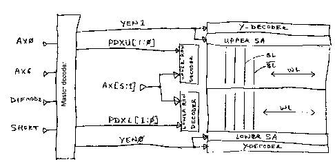
Figure 1 shows a block diagram of the addressing system of the present
invention
employed with a memory block having a folded bitline configuration. The memory
block
includes conventional single transistor and storage capacitor cells (not
shown). Each memory
block is divided into two sub-blocks, each having its own s;et of bitlines,
associated bitline
sense amplifiers and y-decoders. In the dual DRAM cell mode, two wordlines for
each dual
cell connected to a complementary pair of bitlines are activated for read and
write operations.
The conventional bitline sense amplifiers perform differential sensing to read
data from its
associated complementary pair of bitlines. Differential sensing due to the
complementary
data storage of the dual DRAM cell provides improved sensing margins. In
addition, by using
two cells per bit, the retention time is improved. As a result smaller
capacitors can be used
CA 02342516 2001-03-30
-3-
compared with a 1T1C cell. In planar CMOS process, the overall 2T2C cell size
can be made
comparable with 1 T 1 C cell size with still improved retention and SER
characteristics.
Figure 2 shows a more detailed circuit schematic of the Master decoder block
shown
in Figure 1. Row address signals AX[0] and AX[6] axe received by respective D-
type flip
flop circuits, with a common enable input connected to an address enable
signal ADR_EN.
A pair of flip flops receives a differential mode control signal DIF MODE
(DIFMODE port
from Figure 1), a reset signal RESET, a mode enable signal MODE EN, a page
mode
enable signal SHORT PG (SHORT port from Figure 1) and a clock signal CLK.
Signal
DIFMb enables differential mode and SPGb enables short page mode. The D-flip
flop and
flip flop circuits function as registers for the input signals. The remainder
of the circuit
includes standard logic gates such as NAND gates and inverters. The Master
decoder block
controls the upper and lower row decoders such that they each activate two
wordlines
simultaneously in the dual DRAM cell mode, or only on~~ wordline in the normal
single
DRAM cell mode, in response to the DIF MODE control si;~nal.
Figure 3 illustrates a conventional folded bitline DRAM configuration for a
single
transistor and storage capacitor memory cell. In the dual DRAM cell mode, both
wordlines
WLi and Wli+1 are simultaneously activated to enable access to two single
transistor and
storage capacitor memory cells for storing or reading complementary data. For
example,
CELL1 and CELL2 can store logic levels of"1" and "0", or "0" and "1"
respectively.
By using two cells per bit, smaller capacitors can be used to obtain the same
bitline
split as one cell per bit in an ideal situation using 2xC/2, should result in
the same split.
However, there is increased bitline capacitance when using the 2 cell; 2
transistor (2C2T)
cell, and the 2xC/2 rule may not hold true in practical implementation.
A 0.18 micron test chip was measured in both the :L T 1 C and differential
operating
modes, and the results are plotted in Figure 4.
In an alternative embodiment, the dual DRAM cell can store mufti-bit data. For
example, CELL1 and CELL2 can store logic levels of "1" and "1" and "0" and "0"
to store
four possible logic states (two bits per cell) instead of just one.
In yet another alternative embodiment, the dual DRAM cell can store an analog
voltage.
The Master decoder block also receives an additional address or mode bit for
selecting between a long page and a short page mode access in each memory
block within a
CA 02342516 2001-03-30
-4-
memory array. The operation is done on the fly, allowing the user to
dynamically choose
between the addressing modes. In the short page mode access, only one of
either the upper or
lower row decoders is activated. In the long page mode access, both the upper
and lower row
decoders are activated. This feature of the Master decoder block is combined
with the dual
DRAM cell selection feature. More specifically, the dual DRAM or single DRAM
cell
modes can be selected in either the short page mode acce~;s or the long page
mode access.
Therefore, twice the number of bits can be accessed in the long page mode
access over the
short page mode access. The addressing circuit also generates the necessary
enable signals to
ensure that the bitline sense amplifiers and y-decoders of both sub-blocks are
enabled during
the long page access mode.
With reference to the block diagram of Figure 1 both long and short page
access
modes are realised by having the bitlines extending within half of the block,
as shown in
Figure 1. The column decoder is controlled by the decoded local RAS signal
(not shown),
which disables column access if there is no selected column. in the
corresponding part of the
block. As previously discussed, one wordline can be activated in the block, or
both wordlines
can be activated in the block simultaneously, depending o:n the state of the
control signal
SHORT. Therefore, the user can select wide page versus short page addressing
modes on
the fly.
As shown in Figure l, the Master decoder block. receives addresses AX[0) and
AX[6], and control signals DIFMODE and SHORT. The Master decoder block
receives
other signals required for general operation of the circuit, which are not
shown in Figure 1.
These additional signals are shown in Figure 2. Y-decoder enable signals YENl
and YEN2,
predecoded upper and lower row address signals PDXU(1:0) and PDXL[1:0]
respectively
are generated by the Master decoder block. The block diagram of Figure 1 only
depicts one
block out of a plurality of blocks within the entire memory device or embedded
memory
macro, however, one skilled in the art would understand that the other blocks
are similarly
configured to the one shown in Figure 1. The Master decoder block, the upper
row decoder
and lower row decoder are part of the row decoder circuitry for the memory
block.
Additional row decoder circuits can include timing control circuits which are
not shown in
Figure 1.
Address AX[0) is suppressed when the differential mode is enabled. Address
AX[6)
is enabled if the short page mode selected. Upper and lower sense amplifier
enable signals
CA 02342516 2001-03-30
- 5 -
are decoded in the short page access mode. In the short page access mode, the
unaccessed
sub-array of the block remains in stand-by, or low power made to reduce power
consumption.
Although not shown, the data bus circuitry is also configurable depending on
the
selected access mode.
The Master decoder circuit of the present invention has been implemented in a
0.13
micron SoC-RAM PL test chip.
The addressing system of the present invention is not limited to use in DRAM
memories. The present invention can be used with any type of memory such as
Flash,
SRAM, FRAM and EEPROM circuits, for example.
Dual DRAM cell memory according to the present invention is useful for harsh
conditions, mission critical data, or any circumstances in vvhich the user
decides that high
data reliability is required. Alternatively, the system can automatically
select the dual cell
mode when small amounts of data are to be stored, to reduce refresh power
consumption.
The present invention does not require any change in the core memory
architecture or
column decoder circuits. Only row decoding circuits are adjusted to
accommodate the two
different cell storage modes.
This technique can be used in Flash, EEPROM, single-ended SRAM cells, or any
memory that typically employs single-ended sensing using re:E'erence voltages.
The above-described embodiments of the invention are intended to be examples
of the
present invention. Alterations, modifications and variations may be effected
the particular
embodiments by those of skill in the art, without departing ~Crom the scope of
the invention
which is defined solely by the claims appended hereto.