Note : Les descriptions sont présentées dans la langue officielle dans laquelle elles ont été soumises.
CA 02344408 2001-03-14
WO 00/16594 PCT/US99121183
BALLAST CIRCUIT FOR HIGH INTENSITY DISCHARGE LAMPS
FIELD OF INVENTION
This invention relates to high intensity discharge lamps, and more particular,
to a
ballast circuit for a high intensity discharge lamp which is more efficient
and requires
fewer components than previous ballast circuits.
BACKGROUND OF INVENTION
High intensity discharge (HID) lamps provide light by producing an arc between
an anode and a cathode, rather than energizing a filament. These lamps include
do metal
halide lamps and high pressure Xenon lamps which combine high luminance and
good
color retention. Applications include low do input, portable light fixtures
and ac powered
fiber-optic illuminators used for industrial and medical lighting.
Typical ballast circuits take a low input, ac or dc, and amplify the input
over
several stages producing high currents and thus requiring circuits which can
control the
current to provide a more steady current thereby providing a more steady light
output,
i.e. no flickering of the light. However, because these circuits operate at
higher currents,
the circuits must include heavy duty components specially designed to carry
such high
currents which further adds to the expense of producing these circuits.
Moreover,
because the ac voltages include high frequencies, the circuits must protect
against acoustic
arc resonance induced by the high frequencies which further causes the light
to flicker.
By requiring numerous and complex circuits to accommodate the above
requirements, there is a high power loss in the form of heat due to the high
current
CA 02344408 2001-03-14
WO 00/16594 PCT/US99/2I183
2
through so many different circuits. This further requires a means for cooling
the circuit
by a cooling interval before relighting the lamp as well as the need for
actively cooling
the circuits by including fans, further adding to the current consumed by the
circuit to
operate the fans and further increasing the power losses.
As a result, these lamps are neither energy efficient nor inexpensive to
produce
and operate.
SUMMARY OF INVENTION
It is therefore an object of this invention to provide a ballast circuit for a
high
intensity discharge lamp which is more efficient than prior ballast circuits.
It is a further object of the present invention to provide such a circuit
which is
cost effective to implement.
It is a further object of the present invention to provide such a ballast
circuit
which may be produced using standard, inexpensive components.
It is a further object of the present invention to provide such a ballast
circuit
which has much fewer components than prior art ballast circuits.
It is a further object of the present invention to provide such a ballast
circuit
which operates at a lower current than prior art ballast circuits.
It is a further object of the present invention to provide such a ballast
circuit
which produces less heat than prior art ballast circuits.
It is a further object of the present invention to provide such a ballast
circuit
which eliminates flickering induced by high frequencies.
CA 02344408 2001-03-14
WO 00/16594 PCT/US99/21183
3
It is a further object of the present invention to provide such a ballast
circuit
which produces a steady output to eliminate flickering.
The invention results from the realization that a smaller, more compact and
more
efficient ballast circuit for a high intensity discharge lamp can be achieved
by initialling
boosting the input voltage to a higher level, thereby reducing the current to
a
proportionally lower level then further tailoring the voltage for the
transition to the steady
state mode of operation of the discharge lamp to minimize current levels being
manipulated, to reduce power losses to heat, and reduce the number of
components
required and their complexity, and then bucking the voltage back down to the
lower
voltage and proportionally higher current required for operating the lamp.
This invention features a ballast circuit for a high intensity discharge lamp.
There
is a boost converter, responsive to a do input voltage, for providing a
boosted do output
voltage. A boost controller, responsive to the boosted do output voltage,
drives the boost
convener to maintain the boosted output voltage at a predetermined level.
There is a
buck convener, responsive to the boosted do output voltage, for providing a
reduced do
output voltage. A buck controller, responsive to the reduced output voltage,
drives the
buck converter to operate the discharge lamp in a transition mode and maintain
the
reduced do output voltage at a preselected level for operating the discharge
lamp in a
steady state mode.
In a preferred embodiment, the boost converter may include an inverter,
responsive to the do input, for producing an ac output. The boost converter
may include
a step-up transformer, responsive to the ac output, for producing a boosted,
alternating
CA 02344408 2001-03-14
WO 00/16594 PCTNS99/21183
4
output. The boost converter may include a rectifier, responsive to the
boosted,
alternating output, for producing the boosted do output voltage. The buck
controller may
include a variable pulse width generator, responsive to the boosted do output
voltage, for
providing a pulsed, reduced voltage output. The boost converter may include a
resonant
voltage divider, responsive to the reduced, pulsed output, for producing the
reduced
output voltage. The buck converter may include an output filter, responsive to
the
reduced output voltage, for eliminating ripple current, limiting
electromagnetic
interference, and reducing flicker of the discharge lamp. The output filter
may be
incorporated into the resonant voltage divider. There may be an voltage over
protection
circuit, responsive to a voltage differential between the reduced do output
voltage and the
voltage at the lamp, for preventing the variable pulse width generator from
producing the
high voltage, pulsed output. There may be an ignitor, responsive to said
boosted output,
for igniting a high intensity discharge lamp. There may be an input filter,
responsive to
the do input voltage for eliminating noise from the do input voltage.
The invention also features a ballast circuit for a high intensity discharge
lamp
having a boost converter, responsive to a do input voltage, for providing a
boosted do
output voltage, a buck converter, responsive to the boosted do output voltage,
for
providing a reduced do output voltage and a controi circuit, responsive to the
boosted do
output voltage and the reduced do output voltage, for driving, respectively,
the boost
converter to maintain the boosted do output voltage at a predetermined level
and the buck
converter to decrease the boosted output voltage to the reduced output voltage
and
maintain the reduced output voltage at preselected, steady state level.
CA 02344408 2001-03-14
WO 00/16594 PCTNS99/21183
5
DISCLOSURE OF PREFERRED EMBODIMENT
Other objects, features and advantages will occur to those skilled in the art
from
the following description of a preferred embodiment and the accompanying
drawings, in
which:
Fig. 1 is a schematic block diagram of a high intensity discharge lamp system
including the ballast circuit of the present invention comprising a boost
converter circuit,
a buck converter circuit and a controller circuit;
Fig. 2 is a more detailed schematic block diagram of Fig. 1 in which the boost
converter, buck convener and controller circuits are further broken down into
respective
component circuits;
Fig. 3 is a schematic diagram of a boost converter and a portion of the
controller
circuit according to the present invention;
Fig. 4A is a schematic diagram of a trigger circuit used to ignite a high
intensity
discharge lamp having an ignition voltage of less than 10 KV;
Fig. 4B is a schematic diagram of a trigger circuit, similar to Fig. 4A, used
to
ignite a high intensity discharge lamp having an ignition voltage greater than
10 KV;
Fig. 5 is a schematic diagram of a buck converter and the remaining portion of
the controller circuit according to the present invention;
Fig. 6 is a block diagram, similar to Fig. l, in which the input voltage to
the
circuit is ac; and
Fig. 7 is a schematic diagram, similar to Fig. 3, including an electromagnetic
interference (EMI) filter and rectifier for an ac input voltage to produce a
do input.
CA 02344408 2001-03-14
WO 00/16594 PCT/US99/21 t83
6
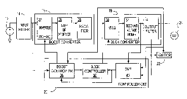
Generally, ballast circuit 10, Fig. 1, includes a boost converter 16, buck
converter 18 and control circuit 20, responsive to both boost convener 16 and
buck
converter 18. Input filter 14 receives do input 12 which may be, for example,
12-24
volts, and filters out noise and ripple which may affect the remainder of
circuit I0. Boost
converter 16 boosts the smoothed do input from filter 14 to a much higher
level, for
example one hundred volts above the operating voltage of high intensity
discharge lamp
24, but typically 160 Vdc which is beyond the EMI threshold in order to avoid
harmonics
which would cause the light to flicker. The EMI threshold is the level of
electromagnetic
interference that would start to cause the arc to move about the electrode
surfaces. The
exact value is dependent on the lamp design.
However, this is not a necessary limitation of the invention, as the novelty
of the
present invention lies in the initial boosting of the input voltage to reduce
current. By
initially boosting the voltage to a much higher level, the current throughout
the circuit is
necessarily and significantly reduced: typical prior art ballast circuits
operate at 10 amps
or higher while with the present invention operation can occur at 2 amps.
Reducing the
current avoids the need for heavy duty, costly components as well as the need
for
additional current controlling circuits and thus not only allows the use of
common, "off
the shelf" components, but also reduces the actual number of components
required. This
also eliminates the need for cooling means such as fan or large heat sinks,
further
reducing the number of components and thus the cost. Moreover, reducing the
current
and the components needed to accommodate higher currents makes the circuit
much more
efficient by reducing I'-R losses.
CA 02344408 2001-03-14
WO 00/16594 PCT/US99/21183
7
The boosted voltage from boost converter 16 is provided to high intensity
discharge (HID) lamp 24 and ignitor 22 which uses the voltage to ignite lamp
24. Once
HID lamp 24 is lit, buck converter 18 transitions the boosted voltage to a
reduced level,
typically the operating voltage of HID lamp 24. Control circuit 20 is
responsive to both
boost converter 16 and buck converter 18 to ensure that proper voltages are
maintained
by controlling the current in the respective converters.
Boost converter 16, Fig. 2, may include inverter 25 which converts the
smoothed
do input from filter 14 to an alternating voltage. This alternating voltage is
thereafter
provided to step-up transformer 26 which boosts the voltage to the
predetermined level,
e.g. 160 volts. The boosted, alternating voltage is then rectified by
rectifier 28 such that
the output of boost converter 16 is a boosted do voltage. As discussed above
with
reference to Fig. 1, this voltage is used to ignite HID lamp 24.
Control circuit 20 may include boost controller 36 which is responsive to the
boosted do output that controls the current in boost converter 16 to maintain
a constant,
boosted do output.
Once lamp 24 has been lighted, the voltage supplied to lamp 24 must be reduced
to the operating voltage of lamp 24. Lighting lamp 24 enables buck converter
18 which
may include variable pulse width generator (VPWG) 30 which initially produces
boosted
pulses to resonant voltage divider 32, but transitions the voltage such that
the voltage
across lamp 24 approaches a steady state voltage, typically the operating
voltage of the
lamp. Resonant voltage divider 32 provides a constant voltage without
harmonics which
would otherwise cause lamp 24 to flicker.
CA 02344408 2001-03-14
WO 00/16594 PCT/US99/21183
8
Output filter 34 controls ripple current to lamp 24 and further limits
electromagnetic interference to provide a constant output from lamp 24 and
also eliminate
flickering of lamp 24. This provides not only constant light but also
increases the life of
lamp 24 and improves its efficiency by improving lamp stability. Lamp
instability
accelerates electrode erosion. The eroded material migrates to the lamp walls,
reducing
light output. A second effect of lamp instability is to cause the control
circuit to
constantly adjust the boost circuit in an attempt to maintain stable
operation. This is
costly in terms of power loss.
Control circuit 20 may also include buck controller 38, which controls the
current
to buck converter 18, and thus lamp 24, to control the reduction of the output
voltage
during the transition from igniting lamp 24 to steady state operation of lamp
24. Buck
controller 38 also provides the signal that enables ignitor circuit 22.
Over voltage protection (OVP) circuit 40 may also be included in control
circuit
20. OVP 40 shuts down the high voltage trigger pulse to ignitor 22 after a
predetermined
period of time in order to protect lamp 24 by sensing the voltage differential
between the
boosted output at the cathode of lamp 24 and the reduced voltage at the anode
of lamp 24.
Once the lamp has ignited, the signal ceases because there is no longer a
differential at
the lamp. If lamp 24 does not ignite, OVP 40 shuts down boost controller 36
which in
turn shuts down buck controller 38 to prevent continuous striking of the lamp.
Input filter I4, Fig. 3, may include for example an LC network, well known in
the art, for smoothing the input to remove any ripple which rnay adversely
affect the
CA 02344408 2001-03-14
WO 00/16594 PCT/US99/21183
9
remainder of circuit 10 and thus lamp 24. Inverter 25 converts the do input to
an
alternating current. Inverter 25 may include transistor Q3 and diode D6 which
form an
oscillator that, in response to the do input, produces an alternating output
at node 42.
The alternating output at node 42 is submitted to step-up transformer 26 which
may include transformer T 1 to produce a boosted, pulsed output at node 44,
typically
boosted to 160 volts to minimize EMI harmonics as discussed above. This 160
volt,
pulsed output is provided to diodes D2 and D3 of rectifier 28 to produce a
boosted (160
volt) do output at node 46.
Series capacitors C 14 and C 15 provide additional filtering to smooth the
boosted
do output at node 46 while resistors R7 and R8 provide a voltage divider to
ensure a
constant voltage across C 14 and C 15 and thus a constant output voltage.
Boost controller 36 of control circuit 20 monitors the current of boost
converter
16 to ensure that boost converter 16 maintains a constant output voltage.
First controller
48, such as a UC3845 pulse width modulation controller available from Unitrode
Integrated Circuits, Merrimack, New Hampshire, drives paired transistors Q1
and Q2
which in turn drive Q3 of inverter 25 discussed above. Controller 48 senses
current on
line 50, which is proportional to the current across the primary windings of
step-up
transformer 26, to maintain a constant voltage level at node 42 and thus
ultimately a
constant boosted do output at node 46. In response to the current sensed on
line 50, first
controller 48 sends a control signal on line 51 to transistors Q 1 and Q2
which drive Q3
thereby adjusting the output voltage accordingly.
At start up, the boosted output voltage generated by boost convener 16 appears
at
CA 02344408 2001-03-14
WO 00/16594 PCT/US99/21183
10
node 46, Fig.4A, of trigger circuit 58 which represents a trigger circuit
requiring a
trigger voltage less than 10,000 volts, for example, where lamp 24 is a metal
halide
lamp. Transistor Q7 directly drives transformer T2 to develop sufficient
voltage across
lamp 24 to create an arc and thus light the lamp.
For applications which require a higher trigger voltage, e.g. greater than 10
KV
such as a high pressure Xenon lamp, trigger circuit S8', Fig. 4B, may include
SIDAC Q7
which charges capacitor C32 to discharge across the gap of transformer T2 into
the
primary winding to ignite lamp 24.
In order to protect the remainder of the circuit if ignition does not occur
and lamp
24 does not light, OVP 40 of control circuit 20 shuts off trigger S8 after a
predetermined
period of time as discussed above. OVP 40, in response to a differential
across lamp 24,
forces first controller 48, Fig. 3, of boost controller 36 to send a control
signal to second
controller S6, Fig. S, to shut down buck controller 38 to prevent continuous
restriking of
lamp 24. If lamp 24 does not ignite, the voltage at node S3, between output
filter 34 and
resistor R14, is high frequency ac voltage. A portion of this voltage is
rectified by Zener
diode D and diode D10. Capacitor C21 and resistor R19 control the amount of
time
required to reach the predetermined voltage provided to optocoupler SS, for
example a
Model 4N3S available from Motorolla, in order to turn on optocoupier SS. Once
turned
on, optocoupler SS generates a high signal trigger to SCR Q6, via Zener diode
D 11. As
SCR Q6 turns on, Vcc pin 7 of second controller S6, which may be a UC3842
pulse
width modulation controller available from Unitrode Integrated Circuits,
Merrimack,
New Hampshire, is pulled to ground via diode D12. In this way, buck controller
38 is
CA 02344408 2001-03-14
WO 00/16594 PCT/US99/21183
11
shut-down which in turn shuts-down boost controller 36.
If, however, lamp 24 ignites, the voltage at node 53 is a do voltage which is
thus
blocked by capacitor C6, preventing current from charging capacitor C21 which
would
otherwise turn on optocoupler 55.
Initially, there is no output at node 52, because lamp 24 is not on and thus
not
conducting. Accordingly, there is no current provided to VPWG 30. Once lamp 24
is
fired, however, second controller 56 of buck controller 38 is enabled by first
controller
48. Second controller 56 thereafter drives transistor Q5 which in turn drives
transistor Q4
of VPWG 30. VPWG 30 turns on, an output appears at node 52 and trigger 58 is
disabled. When the lamp turns on, the voltage between E1 and E2 drops to a
value
below the SIDAC firing voltage and the trigger circuit is disabled.
Buck controller 38 monitors the current on line 55 and controls the voltage
across
resonant voltage divider 32 by sending a control signal from second controller
56 to drive
transistor Q5 which in turn drives Q4 of VPWG 30. The invention uniquely
incorporates
inductor L3 of output filter 34 into resonant voltage divider 32. However,
this is not a
necessary limitation of the invention as individual voltage divider and
filtering circuits
may be implemented as shown in Fig. 2. VPWG 30 transitions the output at node
52 to
reduce the lamp voltage. The pulse width is adjusted in order to provide a
voltage across
C27 which is the voltage lamp 24 requires. Note that the voltage across lamp
24 is the
difference between the voltage at node 46 and node 52. Thus, buck controller
38
monitors the voltage generated at node 52 and transitions the voltage output
at node 52 to
gradually increase the voltage such that the voltage across lamp 24 decreases
and
CA 02344408 2001-03-14
WO 00/16594 PCT/US99/2i 183
12
approaches the preselected operating voltage of the lamp, typically 24 volts.
Once the
operating voltage is achieved, buck controller 38 monitors the current of Q4
as discussed
above to drive QS so that a constant operating voltage appears across lamp 24.
The foregoing has been directed to a do source. However, this is not a
necessary
limitation of the invention as an ac source may also be used. Alternating
current source
12', Fig. 6, such as a typical 110 volt, 10 amp service, may be used to light
lamp 24.
Source 12' provides an alternating input to input filter 14' which rectifies
the ac input and
filters it to reduce electromagnetic interference to the boost converter. The
remainder of
ballast circuit 10 is essentially the same as the circuit discussed above.
Input ac source i 2' provides an alternating voltage to EMI filter and
rectifier 14'.
Input EMI filter and rectifier 14', Fig. 7, may include common mode filter 62
which
further reduces high frequency noise. Filtering is accomplished by EMI filter
62 which
includes capacitor Cl, resistor R2 and windings L1. The signal is rectified by
rectifier 64
which provides a high ripple do output. Rectifier 64 may include, for example
wheatstone
bridge 66 and capacitor C2.
Boost converter 16' includes step up transformer 26' which in this case
includes
boost inductor L2, to boost the do output to the predetermined level as
discussed above with
respect the do circuit of Fig. 3. Because the input voltage is already at 120
volts, the
rectified do voltage need only be slightly boosted to reach the desired 160
volts as discussed
above.
Power is provided to boost controller 36' which includes first controller 48',
for
CA 02344408 2001-03-14
WO 00/16594 PCT/US99/21183
13
example an L6561 power factor controller available from St-Microelectronic,
Phoenix, AZ.
Switch 56 biases controller 48' via biasing circuit 68 which includes
resistors R11 and R12,
capacitors C6, C7 and C10 and diodes D9 and D7.
The input voltage is sensed by input sensing circuit 70 comprised of resistors
R8,
R9 and R10 and capacitor C8. Controller 48', in response to the voltage
sensed, controls
the output voltage with output voltage sensing circuit 72 comprising resistors
R15, R16,
R17 and capacitor C12. To provide a regulated do voltage at capacitor C3 which
in tum
feeds buck converter 18, Fig. 5. The operation of the remainder of the circuit
is the same
as the do portion discussed above.
Although specific features of this invention are shown in some drawings and
not
others, this is for convenience only as each feature may be combined with any
or all of
the other features in accordance with the invention.
Other embodiments will occur to those skilled in the art and are within the
following claims:
What is claimed is: