Note : Les descriptions sont présentées dans la langue officielle dans laquelle elles ont été soumises.
CA 02345390 2001-03-23
WO 00/17863 PCT/US99/22266
MAGNETORESISTIV1~ DEVICES, GIANT MAGNETORESISTIYB
DEVICES AISTD METHODS g'OR MAKING SAME
~ACI~R_OUND OF THF INVEN'rTnu
Field of Invention
The present invention relates to magnetoresistive and
giant magnetoresistive devices, and more particularly to
magnetoresistive (MR) a:nd giant magnetoresistive (GMR) devices
and sensors fabricated using electrochemistry to deposit
resistive material onto a conductive or partially conductive
substrate and to methods for fabricating same.
Descr?pt~on of Related i
Magnetoresistive sensors are traditionally used to read
data (memory) and when used in conjunction with a magnet., to
monitor the position of moving objects. These sensors
15 generally find use in a wide variety of applications,
including navigational, ferromagnetic metal detection and
location, position and proximity sensing, etc. Resistiwe
elements may also be used as switches or relays integrated as
part of, for example, tunable antennas and bipolar MOS type
20 transistors to reduce source to drain current leakage and in
other microelectronic applications requiring resistance
variation.
A magnetoresistive or magnetoresistance (~~MR~~) sensor is
generally made up of electrically connected (or ~~bridged")
25 regions of active material (resistors) that can detect changes
in an applied magnetic field. These regions of active
material have an electrical resistivity that changes as a
function of both the magnitude and the direction of the
magnetic field. In other words, the region of active material
30 acts as a variable resistor when placed in a changing external
magnetic field. The source of this magnetic field can be for
example internal, origin,~ting from a region in close proximity
on the same integrated circuit or external as for example,
from the earth's magnetic field.
1
CA 02345390 2001-03-23
WO 00/17863 PCT/IJS99/22266
The "sensitivity" o:E such resistors is measured as the
ratio of the change in resistivity (OR) to the change in the
magnetic field (DH). Specifically, the magnetic field rotates
the internal magnetization vector in the film, and the varying
angle of this vector with the current flow affects the
resistance. The sensitivity of a particular resistor depends
on both the structural amd chemical composition of the active
material and, in the care of magnetoresistive devices, the
value of the applied field. The region of active material can
comprise several different layers, which are generally
deposited using any numb>er of different deposition techniques.
A typical material for use as the active layers) in MR
devices is an alloy such as one containing, e.g., cobalt,
nickel, copper, or iron. An example of such an appropriate
alloy is one containing 78.5 nickel and 21.5 iron known
generically and sold as PERMALLOY. The alloy PERMALLOY is
useful for MR sensors because it has high magnetic
permeability and electrical resistivity.
In sensor fabrication, a region (or regions) of active
material is formed by depositing thin films of the various
layers onto a substrate, Traditionally these thin films have
been deposited by relat~_vely expensive methods such as vacuum-
based deposition, i.e., sputtering and molecular beam epitaxy
and in some instances by electron beam (E-beam) or chemical
vapor deposition (CVD). Current commercially available MR
sensors are fabricated by using electron beam, or sputtering
techniques to deposit Perrmalloy as an active material on
silicon chips. As a specific example, a prototypical
commercial sensor is manufactured by sputtering to deposit
layers of PERMALLOY (Nil?e) onto a silicon substrate. II1
addition to their expen:~e, resistors manufactured by CVI~,
sputtering, and MBE are difficult to manufacture in high
volume because of the limits on the size of the substrate.
Attempts in the past ha,Te been made at manufacturing resistors
2
CA 02345390 2001-03-23
WO 00/17863 PCT/US99/22266
by other means. These have however resulted in sensors that
are not sensitive nor reliable enough for modern applications.
There are some commerci~~lly used less expensive deposition
techniques, such as mell~-spinning and ball-milling. However,
these techniques are usually restricted to the production of
heterogeneous alloys.
Giant Magnetoresit:ive ("GMR") sensors are made up of
regions of active material and are less sensitive than MR
sensors even though the~~ exhibit larger total changes in
resistance. Some GMR scsnsors are made up of magnetic layers
separated by layers of diamagnetic or non-magnetic material
while others are made o:E granular metals. The change in
resistivity of these materials is attributed in part to
conduction electrons moving across the non-magnetic layers and
the accompanying spin-do=pendent scattering at or near the
layer interfaces. It i;s believed that the in-plane resistance
between two magnetic la:~rers varies approximately as the cosine
of the angle between th~= magnetization in the two layers.
U.S. Patent No. 5,277,991 to Satomi et al. is directed to an
example of such a GMR type material. In Satomi et al.
magnetic and non-magnetic layers are deposited using a
sputtering apparatus onto glass. This fabrication method has
the advantage of using .a large area substrate such as glass
for producing high quantities of sensors, but is nonetheless
still disadvantageous because it requires the use of an
expensive manufacturing technique Csputtering). Daughton, et
al. describe a sensor made up of GMR Material in "Magnetic
Field Sensors Using GMR Multilayer". The Daughton et al.
sensor is fabricated on silicon wafers by using conventional
integrated circuit processing (i.e. doping, masking,
sputtering, etc.). Hence, these sensors are also manufactured
using an expensive technique. Moreover, the manufacturing
process is further limited, in that the relatively small area
of the silicon wafer substrate, limits large-scale production.
3
CA 02345390 2001-03-23
WO 00/17863 PCT/US99/22266
The article by W. Schwarzacher and D.S. Lashmore, _iant
Maanetoresistance in Ele~ctrodPCpQsited Films, IEEE Transactions
on Magnetics, Vo1.32, No. 4, July 1996, suggests that the use
of electrochemical depo.~ition (electrodeposition) would be
considerably simpler and less expensive than other deposition
techniques for laying down thin films. This article, which is
herein incorporated by reference in its entirety, explains
various techniques for electroplating thin metallic films.
In general, electrochemical deposition involves providing
i0 metal ions in a solution. The~ions receive electrons from one
of two electrodes (the cathode) and are thereby reduced to a
solid form that deposits onto some type of substrate material.
An example of a typical electrodeposition half reaction is
shown below:
Cu2-'~aq~ + 2 e- -~ Cu
If more than one species of metal ions is present in the
solution (electrolyte), it is possible to electrodeposit~
alloys as well as pure metals. Schwarzacher et al. produced
GMR materials by electroplating thin metallic films onto
copper plates. However., since the highly conducting copper
substrates short-circuii~ed the GMR materials during electrical
transport measurements, it was necessary to include a
relatively time consuming and impractical step of dissolving
away the copper substral:e before meaningful measurement could
be made. In another ari:icle, M. Alper et al., Gian
Maanetoresistance in ElE~ctrodeposited Sut~erlattices, Appl.
Phys. Lett. 63 (15), 11 October 1993, the use of
Electrodeposited GMR films as sensors for magnetic data
storage is suggested bulgy is also limited by the requirement of
electrodepositing the thin films onto a copper substrate and
the accompanying need t« dissolve the copper substrate to
avoid short circuiting the resistor.
Hence, despite its cost advantages, electrodeposit:ion has
not heretofore been used to fabricate MR or GMR sensors. As
4
CA 02345390 2001-03-23
WO 00/17863 PCT/US99/22266
set forth above, the problems inherent in using this method to
fabricate sensors have in the past been numbered and varied.
In particular, as described above, the technique of
electrodeposition requires that the material be deposited onto
a conductive or partial7.y conductive substrate, such as for
example copper. Since t:he substrate must be conductive, it
has heretofore been comnnercially impractical to form regions
of active material thereon (resistors) without requiring the
step of dissolving away the copper to avoid short circuiting
the active resistive element.
Electroplating methods, as well as electrochemical
treatments and plating apparatus for the electrodeposition of
thin film alloys on a substrate, are well known. For example,
Castellani et al, in U.S. Patent No. 4,103,756, issued ~Tuly
25, 1978, teaches methods and apparatus for electroplating
Permalloy (NiFe) on a substrate. Electrodeposition has also
been used to fabricate magnetic thin films, as for example,
magnetic recording head:. Such recording heads are fabricated
in U.S. Patent No. 4,75ti,816 to Liao et al. The CoFe thin
2o films deposited in Liao et al. have acceptable permeability
for recording purposes. However, these films are not
magnetorestrictive and therefore cannot be used for sensor
manufacture.
The use of electrodeposition in MR or GMR device or
sensor fabrication to dE~posit active resistive material could
enable the relatively inexpensive, rapid production of .Large
quantities of devices o:r sensors on large area substrates such
as glass. However, the necessity of having an appropriately
conductive substrate versus the tendency for such a substrate
to short circuit the resistive material has kept this
technology from being commercially implemented. Additionally,
the inability to deposi~~ and permanently affix appropriate
materials on otherwise auitable substrates has heretofore also
prevented their use. S~~ecifically, it has heretofore been
5
CA 02345390 2001-03-23
WO 00/17863 PCT/US99/22266
virtually impossible to adhere thin films of electrodeposited
metals such as copper onto large scale substrates such as
planar glass that has been appropriately coated with a layer
of conductive or partially conductive material to facilitate
electrodeposition.
Furthermore, because both MR and GMR sensors must readily
determine changes in the magnitude and direction of an applied
magnetic field, it is advantageous to maximize the sensitivity
of the regions of active material that are electrically
interconnected to create the sensor. Such maximization has
heretofore been difficult or impossible to obtain.
In sum, there is a. need for magnetoresistors and
giantmagnetoresistors a.nd devices such as sensors made
therefrom that: (1) can be fabricated in high volume arid at
low cost using electrodeposition techniques and (2) are:
sensitive and reliable enough for the demands of modern
applications.
SUMI~iARY OF THE INVENTION
The aforementioned and other drawbacks, problems, and
limitations associated with the manufacture of conventional
thin film resistors and sensors are overcome according to
exemplary embodiments of the present invention. The present
invention is based, in part, on using electrodeposition
techniques to deposit regions of active (resistive) material
onto a large area conductive (or partially conductive)
substrate to produce reliable as well as low cost MR arid GMR
devices such as sensors.
The present invention also provides thin film
magnetoresistive sensoa=(s) comprised of resistors having a
line pattern wherein tile width of the lines of
magnetorestrictive material making up the resistors is
maximized so as to enhance the sensitivity of the resulting
sensor.
6
CA 02345390 2001-03-23
WO 00/17863 PC'.T/US99/22266
In an exemplary embodiment, an insulated substrate is
covered with a conductive coating. At least one region of
magnetically active material is deposited on the substrate or
conductive coating using electrodeposition. The region of
active material is patterned, using photofabrication to form
variable resistors having a line pattern. These resistors can
detect changes in a magnetic field either resulting from an
external source such as a remote magnet or internal source
such as an adjacent magnetic source on the IC. The resistance
l0 of each resistor changes as a function of the applied field
and its direction.
In another exemplary embodiment, high permeability
material is electroche~r~ically deposited to concentrate the
magnetic flux delivered. to a region of active material. Such
pole pieces or magnetic' flux concentrators are deposited as
either part of the electrodeposition sequence or added at a
later stage.
In another exemplary embodiment, magnetic layers
separated by non-magnetic layers are alternately deposited
onto a conductive substrate using electrochemical deposition
techniques. The magnet:ic/non-magnetic layers are patterned to
form a GMR resistor ha~~ing increased magnitude of resistive
change. For GMR sensors, the layer structures can be
assembled in such a way to produce spin valve behavior.
In some embodiments, the regions of active material are
electrically connected to additional circuits (e. g., voltage
sources, current sources, resistors, and capacitors) or even
directly to a preampli:Eier chip to make up a MR or GMR device
or sensor.
3o The present invenl:.ion also provides a process whereby
magnetically active material is adherently electrodeposited
onto a conductive substrate without electrically short
circuiting the active material. Suitable substrates for use in
the present invention include, but are not limited to indium
7
CA 02345390 2001-03-23
WO 00/17863 PCT/US99/22266
tin oxide (ITO] coated ~3lass, doped silicon, gallium-arsenide,
germanium, or doped diamond.
BRIEF DE;~CRIPTION OF THE DRAWINGS
The foregoing and other objects, features, and advantages
of the present invention will be more readily understood upon
reading the following detailed description in conjunction with
the drawings in which:
Fig. 1 is a cross section of a magnetoresistive layer
[MR] on ITO coated glass,
Fig. 2 is an isolated MR~resistor situated on a ITO
coated glass substrate.
Fig. 3 is a block diagram illustrating the steps for
deposition of magnetically active material [both MR and GMR]
onto ITO coated glass.
Fig. 4 is a cross section of a giant magnetoresistive
(GMR] material electroplated onto ITO coated glass.
Fig. 5 is an isolated GMR resistor sitting on a planar
ITO coated glass substrate.
Fig. 6 is a schem~~tic top view of a complete
2o magnetoresistive (MR) sensor made up of four (4) resistors and
four (4) pole pieces.
Fig. 7 is an optical micrograph (17x magnification) of a
sensor according to the present invention.
Fig. 8 is a schematic of a typical mask for photomasking
the present invention sensors.
DETAILED DESCRIPTION OF PREFERRED EMBODIMENTS
In a preferred embodiment a magnetoresistive device for
detecting a change in a magnetic field in accordance with the
present invention comprises an insulated substrate having at
least one region of lEas than about 2000 A thickness of a
conductive or partial7.y conductive coating disposed thereon.
It is preferable to limit the thickness of the conductive
coating in order to prevent short circuiting problems
8,
CA 02345390 2001-03-23
WO 00/17863 PCT/US99/22266
associated with the app:Lication of resistive material onto
conductive material.
The insulated substrate is preferably planar glass.
Optical quality glass oi= the Glaverbel type is particularly
suitable. However, other suitable materials for the substrate
include, but are not limited to, a member selected from the
group consisting of stainless steel, gallium arsenide and
doped silicon.
The coating on the substrate is preferably selected from
the group consisting of indium~tin oxide (ITO), indium oxide,
and tin oxide and has a resistivity value of from about 10
ohms/square to about 10~~ ohms/square. Indium tin oxide is a
particularly preferred material for use as the coating .in this
invention.
There is at least ~~ne resistor region comprising at least
one layer of from about 0.5 um to about 2 ~m of an
electrodeposited metallic material disposed on each of the
regions) of conductive or partially conductive coating. This
layer is intentionally kept at minimal thickness to prevent
short circuiting of the resistive material deposited thereon.
Suitable metals for use as the metallic material in this
invention include, but are not limited to one or more of
chromium, platinum, gold, palladium, silver, copper and alloys
and combinations thereof, with copper being especially
preferred. The electrodeposited metallic material is at least
substantially permanently affixed onto the coated substrate.
It has heretofore been impossible to obtain this permanent
adherance of the metallic material on a substrate such as TTO
coated glass.
There is a least one layer of from about 15 A to about
30 ~ of an electrodeposited ferromagnetic material disposed on
the layers) of electrc~deposited metallic material. Preferably
there are from about 10 layers to about 100 layers of the
ferromagnetic material. The ferromagnetic material is
s
CA 02345390 2001-03-23
WO 00/17863 PCT/US99/22266
preferably comprised of a member selected from the group
consisting of iron, nicltel, copper, cobalt and alloys and
combinations thereof. :Preferred ferromagnetic metals for use
in this invention include iron and nickel and a preferred
ferromagnetic alloy is permalloy.
Referring now to t:he drawings, Fig. 1 illustrates the
aforedescribed device showing a region of magnetoresistive
material disposed on a planar glass substrate having a
partially conductive coating thereon. Substrate 11 can be of
any shape, thickness, or size. Preferably, substrate 11 has a
thickness of from about 0.8 ~.m to about 14 ~.m and is most
preferably about 0.8 ~.m. to about 2 ~,m in thickness.
As shown in Fig. 1, substrate 11 has conductive coating
12 disposed thereon. Conductive coating 12 is preferably a
thin film or layer of a. metal, oxide, or semiconductor. Thin
metallic layer 13 is disposed on conductive coating 12.
Ferromagnetic material layer 14 is disposed on thin metallic
layer 13.
In a preferred emY~odiment, the deposition of metallic
layer 13 and ferromagnE~tic material layer 14 is performed by
electrochemical deposition. The deposition preferably takes
place in an electrochemical cell (not shown). A typical
electrochemical cell fc~r use in the present invention
comprises a rectangular box made up of polypropylene. A "U"
shaped magnet is affixed on the outside of the box and is of
sufficient strength to provide a magnetic field of between
500-1000 gauss for MR material deposition. Uniformly
distributed across the volume of the cell is a cathode affixed
to one end of the cell and an anode at an opposite end of the
cell exactly parallel to the cathode. A reference electrode
is positioned in close proximity to a center of a cathode
plate. A means of agitating the solution in a very uniform
manner is provided. T'he solution is typically pumped through
appropriate filters anal there is a thermostat for controlling
CA 02345390 2001-03-23
WO 00/17863 P(:T/US99/22266
the temperature affixed. to the cell. These resistors can be
fabricated using electrodeposition cells and techniques known
in the art.
Thin film 13 is a metallic material affixed onto the
conductive coating. Thin film 13 preferably has a thickness of
from about 10 nm to about 200 nm. The metallic material of
thin film 13 is at lea~;t substantially permanently affixed to
the conductive coating, as explained below. For purposes of
this invention substantially permanently affixed is intended
to mean that for all practical purposes the film does not
readily peel off of the: coating on the glass (substrate) .
Copper is a particularly preferred material for use as the
thin film affixed to tree conductive coating.
The second thin film 14 is ferromagnetic material
disposed on the metallic material 13 and as discussed above,
has a preferred thickness of from about 50 nm to about 2000
nm.
Once.the resistive material has been deposited onto the
coated substrate, the resistor regions can be used as they are
or processed further to form a magnetoresistive sensor. An MR
sensor in accordance with the present invention comprises at
least two electrically interconnected resistors on an
insulated substrate having at least two regions of a
conductive or partiall~,r conductive coating disposed thereon.
Each of the resistors making up a sensor in accordance with
the present invention comprises a magneto-resistive device as
earlier described. Thcs resistors are preferably electrically
interconnected in a Whc~atstone Bridge configuration.
The present inveni~ion MR sensor preferably further
comprises at least one pole piece disposed on the coated
substrate. The pole piece preferably comprises a region of
electrodeposited pole ~~iece material disposed on at least one
region of the coated si.zbstrate. The region of
electrodeposited pole ~~iece material is preferably situated
11
CA 02345390 2001-03-23
WO 00/17863 PC.TNS99/22266
relative to the resistors such that the pole piece material
acts to focus a magnetic field onto the resistors without
shielding the resistors from same. In a preferred
configuration the pole piece element focuses the magnetic
field along its axis onto the resistors. Suitable material
for use as pole piece material should preferably be a
permeable material. E~:amples of such suitable pole piece
material include, but are not limited to nickel-iron, cobalt-
iron and combinations thereof .,
In a preferred emr~odiment an MR sensor in accordance with
the present invention comprises at least one pole piece having
a thickness of from about .5 ~,m to about 5 ~Cm thick. The pole
piece preferably comprises at least one layer of from about
0.5 ~m to about 5 ~.m t'nick of metallic material selected from
the group consisting of chromium, platinum, gold, palladium,
silver, copper and alloys and combinations thereof. The pole
piece further comprises at least one layer of from about 15
to about 30 A of an electrodeposited ferromagnetic material.
The electrodeposited ferromagnetic material is preferably
selected from the group consisting of iron, nickel, copper,
cobalt and alloys and combinations thereof and is disposed on
the layers) of metallic material. Hence, in one embodiment
the pole piece is comb>rised of the same material making up the
reistors.
Each of the resif;tors is configured in a linear pattern
having a preferred line width of from about 15 ~m to about 25
Vim. In MR sensors according to the present invention, linear
patterbs having the p~~eferred line width maximize sensitivity
of the sensor. Any given portion of the linear pattern should
be spatially separated from another given portion by a
distance of from about 2 ~.m to about 20 ~.m.
In a preferred evmbodiment the present MR sensor comprises
four magnetoresistive regions (resistors). Each of two of the
four regions are preferably situated on the substrate at an
12
CA 02345390 2001-03-23
WO 00117863 PCT/US99/22266
angle that is about 90° relative to each of the other two of
the four magnetoresistive regions (resistors).
The resistors) are "patterned" and the pole pieces
delineated using multiple steps of photofabrication. In the
present invention, once the metallic layer and the
ferromagnetic layer are electrodeposited onto conductive
coating the resulting resistive material is photo masked with
photo resist in a specific designed pattern such as that shown
for exemplary purposes only in Fig. 8. Photo resist overlays a
portion of the resistive material and protects it from
subsequent etching step>s. The conductive coating, the metallic
layer and the ferrogmac~netic layer in any exposed region are
etched away.
FIG. 6 illustrated a configuration of variable resistors
in a sensor according too the present invention. Region 172,
272, 372, 472 are each one of four resistors, and regions 173,
273, 373, and 473 are ;pole pieces, which also serve as contact
points. As shown in Fig. 6, variable resistors 172, 272, 372,
and 472 are electrically interconnected through pole pieces
173, 273, 373, and 473 in a configuration commonly referred to
as a Wheatstone Bridge. Additionally, contact points for
connecting to an outside circuit can be spot welded or gold
bonded onto the resistive material to connect with packaging
case.
During sensor operation, the contact points should be
electrically connected across a voltage meter, voltage source,
or capacitor (not showrn) .
An MR sensor in accordance with the present invention can
have a hysteresis mea;~urement of about 1 gauss and a
resistance measurement of from about 500 ohms to about 3000
ohms when measured using a Hall probe and applying a constant
current of about 10 ma at a frequency of 1 KHz. Referring
again to Fig. 7, the maximum sensitivity of this specially
designed sensor is along arrow 101 direction. When the sensor
13
CA 02345390 2001-03-23
WO 00/17863 PCT/US99/22266
is exposed to a changing magnetic field 100 in the direction
of 101, the pole pieces 173, 273, 373 and 473 will align the
magnetic flux along their axis and focus the field on
resistors 172 and 372.
For an MR sensor, when a changing magnetic field 100 in
the direction of arrow 101 is applied, the resistor 172 and
372 have a electrical resistance that changes reversely
proportional to the magnitude of the applied magnetic field
100. However, resistor 272 and 472 have a resistance that
to changes proportional to the magnitude of the applied magnetic
field 100. This reverse, MR response function combined with
Wheatstone Bridge circuit increases the sensitivity in this MR
sensor. In some applic<~tions, the pole pieces can be very
thick to focus the magnetic field 100 to the resistors 172 and
372, the sensitivity of resistors 172 and 372 can be largely
increased. In this case, the resistors 272 and 472 are mostly
shielded from magnetic field 100 by the pole pieces 173, 273,
373 and 473.
In another embodiment, this invention is directed to a
giant magnetoresistive device for detecting a change in a
magnetic field. The device comprises an insulated substrate
having at least one region of less than about 2000 A of a
conductive or partially conductive coating disposed thereon.
Preferably the insulated substrate is planar glass having a
thickness of from about 0.8 ~.m to about 2.0 ~,m and the
partially conductive c:oating is indium titanium oxide having a
thickness of from about 0.2 ~Cm to about 2.0 Vim. The coating
has a resistivity value of from about 10 ohms/square to about
100 ohms/square. Alte=rnative coating materials include indium
oxide and tin oxide and alternative substrate materials
include stainless steE~l, gallium arsenide and doped silicon.
There is at leasi~ one resistor region on the coated
substrate. The resis~;.or region comprises at least one layer
of from about 0.5 ~Cm 'to about 1.0 ~.m of an electrodeposited
14
CA 02345390 2001-03-23
WO 00/17863 PC:T/US99/22266
metallic material disposed on each of the regions) of
conductive or partiall~~ conductive coating. The
electrodeposited metallic material is at least substantially
permanently affixed onto the coated substrate. There is at
least one layer couple (multilayer) disposed on the layers)
of electrodeposited met=allic material. Suitable material for
use as the metallic mat=erial includes chromium, platinum,
gold, palladium, silver, copper, aluminum, titanium and alloys
and combinations thereof, with copper being preferred. There
are about 30 to about G00 layer couples and each layer couple
comprises at least one layer and preferably from about 5 to
about 15 layers of from about 20 ~ to about 30 A of
electrodeposited ferromagnetic material in each of said at
least one layer couple and at least one layer and preferably
from about 3 to about 10 layers of from about 8 ~ to about 13
~ of an electrodeposited non-ferromagnetic material. The
number of layer couples, the number and thickness of the
individual layers making up the couples will vary according to
the materials being used and the ultimate use of the resistive
material. For example, when depositing a cobalt/copper
multilayer, it is preferred to have from about 30-100 couples
of layer cobalt and one layer copper.
Suitable ferromagnetic material for use in the present
GMR resistive device includes iron, nickel, copper, cobalt and
alloys and combinations thereof. Example of such
ferromagnetic alloys include Co-Ni-Cu, Ni-Cu, Ni-Fe, Co-Fe,
Co-Ni, Co-Pt, Fe-Rh, with Co-Ni and Co-Ni-Cu being preferred.
The present embodiment also comprises a GMR sensor
comprising an insulate=d substrate having at least two regions
of less than about 2000 A thickness of a conductive or
partially conductive coating disposed thereon. The coating
has a resistivity val,.ze of from about 10 ohms/square to about
100 ohms/square. The=re are at least two and preferably four
electrically intercon=nected GMR resistors configured
CA 02345390 2001-03-23
WO 00/17863 PCT/US99/22266
substantially in accordance with the aforementioned
description. At least t:wo of the resistors are situated on
the substrate. The elec;trical interconnection can be in a
wheatstone bridge configuration.
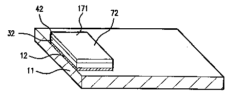
FIG. 4 illustrates a GMR resistor in accordance with the
present invention. Sub:atrate 111 can be of any shape,
thickness, or size. As shown in Fig. 4 the substrate 111 has
conductive coating 112 disposed thereon. As in MR sensar
fabrication, conductive coating 112 is preferably a metal, an
oxide, or a semiconductor. In a particularly preferred
embodiment, the conductive coating is a thin film comprising
indium tin oxide (ITO). The conductive coating has a
preferred resisitivity ~ralue of from about 10 ohms/square to
about 100 ohms/square, ~~nd alternatively can be comprised of
for example, but not limited to, stainless steel, gallium
arsenide or doped silic«n.
Like the MR sensors, the GMR sensors according to the
present invention can further comprise a pole piece element.
Likewise the pole piece element comprises a region of
2o electrodeposited pole piece material disposed on at least one
region of the coated substrate. The region of
electrodeposited pole piece material is situated relative to
the resistors such that the pole piece material acts to focus
a magnetic field onto the resistors without shielding the
resistors from same. Preferably the pole piece focuses the
magnetic field along its axis onto the resistors.
Referring to Fig. 4, in a GMR resistor according to the
present invention, a thin layer of metal 131 is disposed on
the conductive coating 112 and has a preferred thickness of
3o about 10 nm to about 200 nm. The metallic material of layer
131 is at least substantially permanently affixed to the
conductive coating, as explained below. The metallic material
should not be construed. as being limited to copper, but is
preferably selected from the group consisting of chromium,
16
CA 02345390 2001-03-23
WO 00/I'I863 PCT/US99/22266
platinum, gold, palladium, silver, copper and alloys and
combinations thereof.
The active layer 114 is made of a number of alternative
ferro-magnetic and non-'magnetic layers. This multilayered film
114 is disposed directly onto the metallic layer 131. Each
layer of the ferromagnetic material has a preferred thickness
of from about 20 A to about 30 ~1, and preferably comprises a
member of the group consisting of iron, nickel, copper, cobalt
and alloys and combinations thereof. Suitable alloys for use
as the ferromagnetic material include, but are not limited to
a member of the group c~~nsisting of Co-Ni-Cu, Ni-Cu, Ni-Fe,
Co-Fe, Co-Ni, Co-Pt, Fe-Rh, and combinations thereof (see
table 1). Each of the l;~yer(s) of non-ferromagnetic material
has a preferred thickness of about from about 8 A to about 50
is A. Suitable material for use as the non-ferromagnetic
material includes, but :is not limited to a member selected
from the group consisting of copper, silver, platinum,
palladium, titanium, chromium, rhodium and combinations
thereof.
2o In a preferred embodiment, the deposition of multilayer
114 is performed by electrochemical deposition. The relative
thickness of each of these layers influences the sensitivity
relative to the noise o:E the resultant sensor structure. For
example, a copper layer having a thickness of about 12 x1
25 alternating with a coba:Lt layer having a thickness of about 20
A, results in a more sensitive but "noisier" (more hystereses)
sensor than a copper la~Ter having a thickness of about 24 A
alternating with a cobalt layer having a thickness of about
A. The later would be less sensitive than the former and
would typically respond linearly with the magnetic field.
Once layers 131 is electrodeposited onto the conductive
coating, it is peeled oj_f and layer 131 is replated on the
conductive surface thereby substantially, permanently affixing
this layer onto this substrate. A similar photo masking
17
CA 02345390 2001-03-23
WO 00/17863 PCT/US99/22266
process as that describ~sd for the MR sensors above is carried
out on the GMR sensor m<~terial.
Referring now to F:ig. 3, in the case of a GMR sensor, a
relatively thick (from about 1.0 ~,m to about 3.0 pm) pole
piece would be necessar~,r to shield the resistor 272 and 472
from magnetic field 100,, because all four resistors 172, 272,
372 and 472 have the same response function to the magnetic
field 100 (as shown in 1~ig. 6).
In GMR sensors in accordance with the present invention
resistors 272 and 472 can be replaced by constant resistors to
balance the bridge circuit. In this case, the two balancing
resistors 272 and 472 are optionally situated on a circuit
board or integrated into a preamplifier circuit when such GMR
sensors are used therew.Lth.
is Referring now to F_Lg. 3 which schematically illustrates a
process for fabricating a sensor in accordance with the
present invention. Conductive material coated substrate 11
(as shown in Fig. 1) substrate is used for electrochemical
deposition. Tthe size oi= substrate 11 is primarily limited
only by the size of the electrochemical cell in which the
electrodeposition step us performed.
In a preferred embodiment, the substrate co prises
Glaverbel-type glass haring a thickness that is about 1..1 ~m
and a coating thereon comprising indium tin oxide having a
thickness from about .0:?~.m to about 0.2 ~,m and a resistivity
value of from about 10 t:o about 100 ohms per centimeter.
Pre-cleaner 10 prepares substrate 11 and conductive
coating 12 for electrochemical deposition thereon. Each
substrate is cleaned using ultrasonic cleaning, de-ionized
3o water, and an acid solution. Each substrate is attached to an
electric contact and a copper loop.
A thin metallic la~~er 131 (shown in Fig. 4) is
electrochemically deposited onto conductive coating 112. In a
preferred embodiment, train film depositor 20 comprises an
18
CA 02345390 2001-03-23
WO 00/17863 PCT/US99/22266
electrochemical cell and a copper electrolyte. Thin film
depositor 20 deposits at least one first layer (not shown) of
from about 0.01 ~m to about 0.2 ~,m of copper onto the
conductive coating on the substrate. A film peeler (not
shown) peels off the at least one first metal layer.
Alternatively, the substrate is removed from the
electrochemical cell and the first metal layer is peeled off
by hand. The substrate is placed back in the cell and thin
film depositor 20 deposits preferably from about 10 nm to
about 200 nm of at least one second layer of copper onto the
region on conductive coating 112 from which the first layer of
copper is peeled so as to provide requisite electrical
conductivity for further deposition. This second layer of
copper is thereby substantially permanently affixed to the
coated glass.
Magnetically active material depositor 30 deposits at
least one thin film of magnetoresistive material 14 (shown in
FIG. 1) onto the thin metallic layer 13. In order to make MR
sensors, active material depositor 30 comprises an
electrochemical cell and a solution for depositing a single
magnetic element or magnetic alloy. In a preferred
embodiment, the magneti~~ allay comprises nickel and iron.
Magnetoresistive material depositor 30 preferably deposits
between 50nm and 2000nm of the magnetic alloy onto thin film
13. GMR deposition includes providing a substrate having a
conductive coating thereon requires an additional step wherein
a thin film. depositor deposits a layer of non-ferromagnetic
material alternatively with the ferromagnetic material being
deposited.
The present invention is also directed to a method for
electrodepositing magnetoresistive material onto an insulated
substrate and at least substantially permanently affixing same
thereon. The method comprises the steps of providing an
insulated substrate having a conductive or partially
19
CA 02345390 2001-03-23
WO 00/17863 PCT/US99/22266
conductive coating to a thickness of from about 0.2 ~.m to
about 2.0 ~m thereon and electrodepositing at least one first
layer of metallic mater:i.al onto at least one region of the
conductive or partially conductive coating. The conductive or
partially conductive co~~ting is selected from indium tin oxide
(ITO), indium oxide, and tin oxide, with indium tin oxide
being preferred. The first layer has a preferred thickness of
from about 0.5 ~m to about 2.0 Vim. Preferred material far use
as the metallic materia:L in the present invention includes,
but is not limited to chromium, platinum, gold, palladium,
silver, copper and alloys and combinations thereof, with
copper being preferred.
The next step comprises removing the first layer of
metallic material from conductive or partially conductive
coating. After removing the first layer, a second layer of
metallic material having a thickness of from about 0.5 ~.m to
about 2.0 ~.m is electrodeposited onto the regions) of
conductive or partially conductive coating. At least one
layer of magnetoresistive material is electrodeposited onto
the second layer of metallic material. The preferred manner in
which to remove the fir~~t layer of metallic material is by
peeling it off the coated substrate. A magnetic field should
preferably be provided during the electrodeposition steps, the
value of the magnetic field is preferably from about 500 gauss
to about 2 kilo-gauss.
In a further embodiment, the present invention is
directed to a method for- producing a sensor. The method
comprises providing an insulated substrate having a conductive
or partially conductive coating disposed thereon. A layer of
from about 0.5 ~m to about 2.0 ~,m of copper is at least
substantially permanently affixed on the conductive or
partially conductive co~~ting. At least one layer of from
about 15 A to about 30 F~ of ferromagnetic material is
electrodeposited onto the layer of copper. At least one
CA 02345390 2001-03-23
WO 00/17863 PCT/LIS99l22266
portion of the ferromagnetic material and the copper layer and
conductive or partially conductive coating are etched away
thereunder to thereby form at least two spatially separated
regions of active material. Fig. 5 illustrates a GMR resistor
in accordance with the present invention. Each of the regions
of active material are then interconnected in an electrical
bridge configuration.
In this method the substrate has a preferred thickness of
from about 0.8 ~m to about 2 ~.m. The conductive or partially
conductive coating is selected~from the group consisting of
indium tin oxide (ITO), indium oxide, and tin oxide, with
indium tin oxide being F~referred.
The step of electrodepositing at least one layer of
ferromagnetic material onto the layer of copper comprises
electrodepositing from about 10 mono-layers to about 100
layers of one of the group consisting of iron, nickel, copper,
cobalt and alloys and combinations thereof. Nickel and the
alloy permalloy are preferred.
The method can further comprise forming at least pole
piece on said substrate by forming a region of
electrodeposited pole piece material on the conductive or
partially conductive coating. The region of electrodeposited
pole piece material is situated such that it acts to focus a
magnetic field being applied to the device onto the
magnetoresistive regions) without shielding it from same.
Preferably the pole piece element focuses the magnetic field
along its axis onto the magnetoresistive region(s). The pole
piece is preferably percr~eable and selected from the group
consisting of nickel-iron, cobalt-iron and combinations
thereof.
In yet another embodiment, the present invention is
directed to a method of making a giant magnetoresistive device
for detecting a change in a magnetic field. The substrate and
substrate coating are the same as those used in MR device
21
CA 02345390 2001-03-23
WO 00/17863 PCT/US99/22266
fabrication. At least one resistor region is produced. The
steps for depositing the GMR resistor comprise
electrodepositing at least one layer of from about 0.5 ~,m to
about 1.0 ~m of a metallic material on each of the region of
conductive or partially conductive coating on the substrate.
The metallic material is at least substantially permanently
affixed thereto. At least one layer couple is
electrodeposited onto the at least substantially permanently
affixed layer of electrodeposited metallic material. Each of
l0 the layer couples) comprises at least one layer of from about
20 A to about 30 A of a ferromagnetic material and at least
one layer of from about 8 ~ to about 13 ~ of an non-
ferromagnetic material. The ferromagnetic material is
comprised of a member selected from the group consisting of
iron, nickel, copper, cobalt and alloys and combinations
thereof. The alloys are selected from the group consisting of
Co-Ni-Cu, Ni-Cu, Ni-Fe, Co-Fe, Co-Ni, Co-Pt, Fe-Rh, and
combinations thereof, with Cu-Ni and Co-Ni-Cu being preferred.
The non-magnetic material is preferably selected from copper,
silver, platinum, palladium, titanium, chromium, rhodium and
combinations thereof.
This method comprises electrodepositing from about 30 to
about 100 layer couples onto the layer of electrodeposited
metallic material. This method, like the one for fabricating
the MR sensors can further comprise the step of forming at
least one pole piece being situated relative to the giant
magnetoresistive region such that the pole piece material acts
to focus a magnetic field being applied to the device onto the
giant magnetoresistive regions) without shielding the region
from same.
In order to fabricate a GMR resistor device and a sensor
made therefrom according to the present invention, the active
material is deposited in an electrochemical cell 30. An
22
CA 02345390 2001-03-23
WO 00/17863 PCT/US99/22Z66
electrolyte solution of cobalt sulfamate, copper sulfate and
boric acid.
In an altern~~tive method for depositing pole-pieces,
there is a multi-;step photo masking process (1). In this
process photo resist will cover the whole surface of active
layer and a window will be open only in pole pieces region
173, 273, 373 and 473 as shown in Fig. 6 to enable the
deposition of add:Ltional pole piece layer through the windows.
The pole piece depositor 50 deposits pole piece material
on the active layE~r in the open regions. Pole piece depositor
50 can be the samcs or different electrochemical cell as active
magnetic layer depositor with a solution for depositing a
single magnetic e:Lement or magnetic alloy. The thickness of
the pole piece la~~er varies from about 0.1 ~.m to 5 about ~,m.
A photo resi;3t cleaner cell 60 is used to remove the
photo resist on the surface after pole piece deposition.
Photo masking process (2) 70 will mask the sample as the
final pattern sho~Ned in Fig. 6.
The etcher 8i) is responsible for removing regions between
resistor lines and the region between the pole pieces as shown
in Fig. 6. It is preferable to remove all conductive materials
in the region menl:.ioned, including active layer 14 for MR
sensors and 114 for GMR sensors, conductive layer 13 and ITO
layer 112. The enchant used in etcher 80 can be one or several
in sequence to etch the metallic layers and ITO layer. If
conductive coatinc3 12 is not removed, variable resistor is not
insulated from adjacent variable resistors (not shown). When
a variable resistor is electrically connected to additional
circuits to form ~~ sensor, the underlying ITO layer becomes a
path for electrical current, the current in adjacent resistor
lines will conduct. laterally instead of along the path of
lines making up the resistor. The reduced current that
results along the intended path decreases the overall
effectiveness of the sensor.
23
CA 02345390 2001-03-23
WO 00/17863 PCT/US99/22266
The scriber 90 is responsible for making final cuts, if
necessary, to the substrate 11. The scriber 90 should make
whatever cuts are necessary to prepare substrate 11 and the
resistors formed thereon for use in the ultimate application.
s Finally, the individual sensors will be packed in step
100.
Numerous variations or modifications of the disclosed
invention will be evident to those skilled in the art. While
the foregoing description makes reference to particular
illustrative embodiments, this patent is intended to cover all
variations or modifications that do not depart from the spirit
and scope of the disclosed invention.
ExArsPLEs
Example 1 - Electrod~eposition and Photofabrication for MR
Sensor
1. Substrate:
Glass type: Glaverbel
Thickness: 1.1 ~,m
ITO Coating: 15 ohms/square
2. Pre-clean steps:
a) Samples preparation: the ITO glass is cut into
3.5" x 3.5" squares, electrical contact with a copper loop is
made around a 3" diameter deposition window isolated from the
electrolyte with electroplating tape.
b) Pre-deposition cleaning:
ultra;~onic cleaning: 4 Oz/Gal Micro, 50°C, 3min
rinse with deionized water: 50°C, 3 min
dip into 2.5~ H2S04 etching for 1 min.
Rinse with D.I. water.
3. Copper deposition:
a) electrolyte for copper conductive layer
deposition:
copper pyrophosphate strike solution: 333 ml/L;
water: 666 ml/L;
pH : 8 . 8
24
CA 02345390 2001-03-23
WO 00/17863 PCT/US99/22Z66
b) deposition condition:
Anode: Cu
Plating potential: potentiostatic deposition at
-2.OV SCE (saturated calomel electrode)
Temperature: ambient
Cathode and anode are kept parallel to achieve
uniform film layer thickness
c) copper layer deposition and bonding treatment:
50 nm of Cu are deposited on the prepared and
cleaned ITO glass, the glass is then blown dry; scotch tape is
used to remove the Cu film, the glass is etched with 2.5~ HZS04
and is rinsed with deionized water; the deposition procedure
is repeated until a final thickness of the Cu layer on ITO
glass is 45 nm as measured by coulombmeter.
4. Permalloy layer deposition:
Electrolyte:
Nickel sulfamate 315m1/L;
Ascorbic Acid (antioxidant) 6g/L
Iron sulfavmate: 30 rnl/L
2o Boric acid: 30g/L
Saccharin: 2g/L
Temperature: 50°C
pH: 2.0
Applied field: 600 gauss parallel to the film
surf ace ;
No stirrin!~ during deposition. The permalloy is
electro-deposited to a layer thickness of 250 nm as measured
by a coulometer
5. Photo-etchin~~
a) Cleanin<~: the sample is rinsed with Acetone,
Isopropanol and D.I. water while sample is placed on a spinner
at low spin speed 0500 RPM) for a total of 60 second; then
spin dried at 4000 Rl?M for 60 seconds.
CA 02345390 2001-03-23
WO 00/17863 PCT/US99/22266
b) the sample is baked in an oven at 120°C for 15
minutes. The sample is allowed to cool for 3 minutes.
c) photo-resist is spun on (Shipley, Inc. #1813):
set time and speed as 6 sec at 700 RPM followed by
60 seconds at 4000RPM
d) the sample is baked in an oven for 20 minutes at
120°C, then is allowed to cool for 3 minutes;
e) the sample is masked, aligned and exposed to W
light at l5mV/cm2 (setting on the exposure meter for 14
l0 seconds ) .
f) developing: sample is placed back on spinner and
developer is poured ~~n at stopping mode for 60 seconds, the
spin cycle is turned on, the sample is spun at low speed
(500RPM) with develo~~er and water for 10 extra seconds
followed by water fo:r 55 seconds. The sample is subjected to
a high speed spin (4000RPM) for 1 minute to dry.
g) the sam~~le is hard baked at 120°C for 20 minutes.
6. Etching:
a) solution:
1 part: FeCl3 50g/1
1 part: HCl 3 7 ~
50°C
b) sample submerged for 10 seconds
c) sample baked at 150°C for 5 minutes
d) sample resubmerged in etchant for 2 more minutes
e) sample rinsed with acetone to remove mask
7. Scribing:
The sample is cut into individual sensor elements
using a commercial s7.icing saw. The glass is taped from the
glass side and is cut: using wheel lOPBM050A. Fig. 6 is an
optical micrograph of a sensor made in accordance with this
example.
Example 2 - GMR resie~tor and sensor fabrication
1. Substrate:
26
CA 02345390 2001-03-23
WO 00/17863 PCTNS99/22266
Glass type: Glaverbel
Thickness: 1.1 ~,m
ITO Coating: 15 ohms/square
2. Pre-clean steps:
a) Samples preparation: the ITO glass is cut into
3.5" x 3.5" squares, electrical contact with a copper loop is
made around a 1" dianneter deposition window isolated from the
electrolyte with elecaroplating tape.
b) Pre-deposition cleaning:
ultra:ronic cleaning: 4 Oz/Gal Micro, 50°C, 3min
rinse with deionized water: 50°C, 3 min
dip into 2.5~ HZS04 etching for 1 min.
Rinse with D.I. water.
3. Copper deposition:
a) electrolyte for copper conductive layer
deposition:
copper pyrophosphate strike solution: 333 ml/L;
water: 666 ml/L;
pH: 8.8
b) deposition condition:
Anode; Cu
Plating potential: potentiostatic deposition at
-2.OV SCE (saturated calomel electrode)
Temperature: ambient
Cathode and anode are kept parallel to achieve
uniform film layer thickness
c) copper layer deposition and bonding treatment:
50 nm of Cu are deposited on the prepared and
cleaned ITO glass, the glass is then blown dry; scotch tape is
used to remove the Cu film, the glass is etched with 2.5~ HZS04
and is rinsed with deionized water; the deposition procedure
is repeated until a final thickness of the Cu layer on ITO
glass is 45 nm as measured by coulombmeter.
4. GMR multilayer deposition:
27
CA 02345390 2001-03-23
WO 00/17863 PCT/US99/ZZ266
Electrolyte:
cobalt sulfam~~te 500 ml/L;
copper sulfate: 2.947 g
Boric acid: 30g/L
Water: 500m1
Temperature: ambient
pH: 2.2
cobalt cathode. charge potential -1.8V
copper cathodes charge potential -0.26V
cobalt plated to 20 A, shut power wait 3 seconds
copper plated to 9 ~.
S. Photo-etching
a) Cleaning: t:he sample is rinsed with Acetone,
Isopropanol and D.I. wager while sample is placed on a spinner
at low spin speed (-.500 RPM) for a total of 60 second; then
spin dried at 4000 RPM i:or 60 seconds.
b) the sample is baked in an oven at 120°C for 15
minutes. The sample is allowed to cool for 3 minutes.
c) photo-resi~at is spun on (Shipley, Inc. #1813):
set time and :peed as 6 sec at 700 RPM followed by
60 seconds at 4000RPM
d) the sample is baked in an oven for 20 minutes at
120°C, then is allowed t:o cool for 3 minutes;
e) the sample is masked, aligned and exposed to UV
light at lSmV/cm2 (setting on the exposure meter for 14
seconds).
f) developing: sample is placed back on spinner and
developer is poured on at stopping mode for 60 seconds, the
spin cycle is turned on, the sample is spun at low speed
(500RPM) with developer and water for 10 extra seconds
followed by water for 5~~ seconds. The sample is subjected to
a high speed spin (4000F:PM) for 1 minute to dry.
g) the sample is hard baked at 120°C for 20 minutes.
6. Etching:
28
CA 02345390 2001-03-23
WO 00/17863 PCT/US99/22266
a) solution:
1 part FeCl3 50g/1
1 part HC1 37%
50°C
b) sample submerged for 10 seconds
c) sample baked at 150°C for 5 minutes
d) sample resubmerged in etchant for 2 more minutes
e) sample rinsed with acetone to remove mask
7. Scribing:
The sample is cut into individual sensor elements
using a commercial slicing saw. The glass is taped from the
glass side and is cut using wheel lOPBM050A.
Many different .embodiments of the present invention may
be constructed without departing from the spirit and scope of
the present invention. It should be understood that the
present invention is not limited to the specific embodiments
described in this sp~=_cification. To the contrary, the present
invention is intended to cover various modifications and
equivalent arrangements included with the spirit and scope of
2o the claims. The fol:Lowing claims are to be accorded a broad
interpretation so as to encompass all such modifications and
equivalent structure, and functions.
29