Note : Les descriptions sont présentées dans la langue officielle dans laquelle elles ont été soumises.
CA 02348851 2001-04-30
WO 00/31314 PC'T/US99/25273
DIAMOND COATED CUTTING TOOLS AND METHOD OF MANUFACTURE
BACKGROUND OF THE INVENTION
The invention pertains to a cutting tool
which has a cobalt cemented tungsten carbide substrate
with a strongly adherent diamond coating thereon.
In the past, brazed-on polycrystalline
diamond (PCD) tipped cutting inserts and cutting
inserts, which had have a chemical vapor deposition
(CVD) diamond coating, have been used for material
removal in certain applications. The workpiece
materials for these material removal applications
included free-machining aluminum alloys, high silicon
aluminum, nonferrous materials (e. g., copper, bronze,
and brass), ceramics materials, fiber-reinforced
materials, graphite laminates, nylons, acrylics,
phenolic resin materials, metal matrix composites
(e. g., silicon carbide or alumina in an aluminum
matrix), plastic, rubber and wood. While these PCD
cutting inserts performed acceptably, these cutting
inserts had an inherent disadvantage in that there was
only one cutting edge per cutting insert. This was in
contrast to a CVD diamond coated cutting insert which
had multiple cutting edges, such as shown in U.S.
Patent No. 5,585,176 to Grab et al. (assigned to
Kennametal Inc. of Latrobe, Pennsylvania, the assignee
of the present patent application). While these earlier
CVD diamond coated cutting inserts have performed in an
acceptable fashion, there remains the need to develop
CA 02348851 2001-04-30
WO 00/31314 PCT/US99/25273
-2-
other processes to produce diamond coated cutting
inserts, as well as diamond coated cutting inserts
produced by these other processes, which possess the
requisite properties to perform in a satisfactory
fashion. These properties include that the coating be
strongly adherent to the substrate so as to avoid
premature flaking, that the thickness of the coating be
sufficiently great so as to provide for adequate tool
life, and that the sharpness of the cutting edges being
sufficiently sharp so as to provide for an acceptable
workpiece surface finish (i.e., an acceptable surface
roughness) .
SUMMARY OF THE INVENTION
In one form thereof, the invention is a
coated body which has a substrate made of tungsten,
carbon, and cobalt. The substrate presents a surface.
Eta phase is present at the surface of the substrate.
Fibrous tungsten carbide grains are present at the
surface of the substrate. The surface of the substrate
has a surface roughness, Ra, of greater than about 12
microinches. A coating layer is on the surface of the
substrate.
In another form thereof, the invention is a
process for making a coated body comprising the steps
of: providing a substrate comprising tungsten, carbon
and cobalt wherein the substrate has at least one
surface with eta phase thereon; subjecting the
substrate with eta phase on the surface thereof to a
conversion treatment at a temperature between about
1250°C and about 2000°C under at least a partial vacuum
for a duration sufficient as to convert at least a
portion of the eta phase to fibrous tungsten carbide
grains whereby the fibrous tungsten carbide grains are
at the surface so that the substrate surface presents a
surface roughness, Ra, of greater than 12 microinches;
and applying a coating to the surface of the substrate.
CA 02348851 2001-04-30
WO 00/31314 PCT/US99/25273
-3-
In still another form thereof, the invention
is a process for making a coated body comprising the
steps of: providing a substrate comprising tungsten,
carbon and cobalt; the substrate presenting at least
one surface; and the substrate having been subjected to
a roughening heat treatment so as to cause grain growth
of the tungsten carbide grains so that the surface of
the substrate has a surface roughness, Ra, of at least
12 microinches, and the roughening heat treatment
causing the reduction of the concentration of the
cobalt at the surface of the substrate; oxidizing the
surface of the substrate which has been subjected to
the roughening heat treatment so as to form eta phase
at the surface of the substrate; subjecting the
substrate with eta phase at the surface thereof to a
conversion heat treatment at a temperature between
about 1250°C and about 2000°C under at least a partial
vacuum for a duration sufficient as to convert at least
a portion of the eta phase to fibrous tungsten carbide
grains so that the fibrous tungsten carbide grains are
at the surface wherein the substrate surface presents
a surface roughness, Ra, of greater than
12 microinches; and applying a coating to the surface
of the substrate.
BRIEF DESCRIPTION OF THE DRAWINGS
The following is a brief description of the
drawings that form a part of this patent application:
FIG. 1 is an isometric view of a coated
cutting insert of the present invention;
FIG. 2 is a cross-sectional view of a corner
of the cutting insert of FIG. 1;
FIG. 3 is an X-ray diffraction (XRD) pattern
of the top face of a diamond coated cutting insert of
Composition No. 1 of Table I which was processed
according to Process No. 2 of Table II and diamond
coated via the hot filament technique so as to be like
CA 02348851 2001-04-30
WO 00/31314 PCT/US99I25273
-4-
Example No. 2 of Table IV and wherein the presence of
eta phase (Co3W3C), diamond, tungsten carbide (WC) and
solid solution carbide (SSC) are noted by the
corresponding peaks [M6C];
FIG. 4 is an X-ray diffraction pattern (XRD)
of the top rake face of a diamond coated cutting insert
of Composition No. 1 of Table I which was processed
according to Process No. 2 of Table II and diamond
coated via the arc jet technique so as to be like
Example No. 4 in Table IV and wherein the presence of
eta phase (Co3w3C) [M6C], tungsten carbide, solid
solution carbide (SSC), and diamond are noted by their
corresponding peaks;
FIG. 5 is an X-ray diffraction (XRD) pattern
of the top rake face of a diamond coated cutting insert
of Composition No. 1 of Table I processed according to
Process No. 3 of Table II and diamond coated via the
arc jet technique so as to be like Example No. 6 of
Table IV and wherein the presence of eta phase (Co3W3C)
[M6C], tungsten carbide, solid solution carbide (SSC),
and diamond are noted by their corresponding peaks;
FIG. 6 is an X-ray diffraction pattern of the
rake face of an uncoated substrate of the cobalt
cemented tungsten carbide of Composition No. 1 of
Table I which was processed according to Process No. 2
of Table II and wherein the presence of eta phase
(Co3W3C), solid solution carbide (SSC), and tungsten
carbide are noted by their corresponding peaks;
FIG. 7 is an X-ray diffraction pattern of an
uncoated substrate of cobalt cemented tungsten carbide
of Composition No. 1 of Table I which was processed
according to Process No. 1 of Table II and wherein the
presence of eta phase (Co3W3C) [M6C], tungsten carbide,
solid solution carbide (SSC), and a trace of graphite
are noted by their corresponding peaks;
FIG. 8 is an X-ray diffraction pattern of a
diamond coated cutting insert of Composition No. 1 of
CA 02348851 2001-04-30
WO 00/31314 PCT/US99/25273
-5-
Table I processed according to Process No. 1 of
Table II and diamond coated via the hot filament
technique so as to be like Example No. 1 in Table IV
and wherein the presence of eta phase (Co3W3C) [M6C],
tungsten carbide, solid solution carbide (SSC), and
diamond are noted by their corresponding peaks;
FIG. 9 is an X-ray diffraction pattern of a
diamond coated cutting insert of Composition No. 1 of
Table I processed according to Process No. 1 of
Table II and diamond coated via the arc jet technique
so as to be like Example No. 3 in Table IV and wherein
the presence of eta phase (Co3W3C) [M6C), tungsten
carbide, a trace of graphite, and diamond are noted by
their corresponding peaks;
FIG. 10 is an X-ray diffraction pattern of a
diamond coated cutting insert that is like Convent.
No. 2 in Table IV and wherein the absence of eta phase
is noted, as peaks due to solid solution carbide (SSC),
tungsten carbide, and diamond are observed;
FIG. 11 is a scanning electron microscope
(SEM) photomicrograph which depicts secondary electron
images (SEI) at a magnification of 1000X of the edge of
the uncoated substrate of a cutting insert of
Composition No. 2 of Table I which was processed
according to Process No. 2 of Table II;
FIG. 12 is a scanning electron microscope
(SEM) photomicrograph which depicts secondary electron
images (SEI) at a magnification of 5000X of the edge of
the uncoated substrate of the cutting insert of
FIG. 11;
FIG. 13 is a scanning electron microscope
(SEM) photomicrograph which depicts secondary electron
images (SEI) at a magnification of 10,000X of the edge
of the uncoated substrate of the cutting insert of
FIG. 11;
FIG. 14 is a graph which displays the results
of a SEM energy dispersive line scan analysis (EDS) at
CA 02348851 2001-04-30
WO 00/31314 PCT/US99/25273
-6-
a 1000X field of the surface of the cutting insert of
FIG. 11 at its edge wherein the peaks represent
tungsten (W), cobalt (Co), and carbon (C) where
indicated;
FIG. 15 is a scanning electron microscope
(SEM) photomicrograph which depicts secondary electron
images (SEI) at a magnification of 10,000X of the
center of the uncoated substrate of the cutting insert
of FIG. 11;
FIG. 16 is a graph which displays the results
of a SEM energy dispersive line scan analysis (EDS) at
a field of 1000X of the surface of the cutting insert
of FIG. 11 at its center wherein the peaks represent
tungsten (W) and titanium (Ti) where indicated;
FIG. 17 is a scanning electron microscope
(SEM) photomicrograph which depicts secondary electron
images (SEI) at a magnification of 5000X of the edge of
the uncoated substrate of a cutting insert of
Composition No. 1 (Table I) processed according to
Process No. 2 (Table II);
FIG. 18 is a graph which displays the results
of a SEM energy dispersive line scan analysis (EDS) at
a 1000X field of the cutting insert of FIG. 17 at its
edge wherein the peaks represent tungsten (W) and
cobalt (Co) where indicated;
FIG. 19 is a scanning electron microscope
(SEM) photomicrograph which depi~~ts secondary electron
images (SEI) at a magnification of 7300X of the edge of
the cutting insert of FIG. 17 and wherein the box
designated with Arrow A designates the location of the
spot EDS analysis set forth in FIG. 20 hereof and the
box designated with Arrow B designates the location of
the spot EDS analysis set forth in FIG. 21 hereof;
FIG. 20 is a graph which displays the results
of a SEM energy dispersive line scan analysis (EDS) of
the area encompassed by the box designated with
CA 02348851 2001-04-30
WO 00/31314 PCT/US99/25273
_7_
Arrow A, wherein the peaks represent tungsten (W),
cobalt (Co)~ and carbon (C) where indicated;
FIG. 21 is a graph which displays the results
of a SEM energy dispersive line scan analysis (EDS) of
the area encompassed by the box designated with
Arrow B, wherein the peaks represent tungsten (W),
cobalt (Co), and carbon (C) where indicated;
FIG. 22 is a scanning electron microscope
(SEM) photomicrograph which depicts secondary electron
images (SEI) at a magnification of 5000X of the surface
of the center section of the cutting insert shown in
FIG. 17;
FIG. 23 is a graph which displays the results
of a SEM energy dispersive line scan (EDS) analysis of
the cutting insert of FIG. 22 at its center section
wherein the peaks represent tungsten (W) and cobalt
(Co) where indicated;
FIG. 24 is a scanning electron microscope
(SEM) photomicrograph which depicts secondary electron
images (SEI) at a magnification of 1000X of the surface
near the edge of a cutting insert of Composition No. 1
(Table I) processed according to Process No. 1
(Table II);
FIG. 25 is a scanning electron microscope
(SEM) photomicrograph which depicts secondary electron
images (SEI) at a magnification of 5000X of the surface
near the edge of the cutting insert of FIG. 24;
FIG. 26 is a graph which displays the results
of a SEM energy dispersive line scan (EDS) analysis at
a 200X field of the surface of the edge of the cutting
insert of FIG. 24, wherein the peaks represent
tungsten (W) and carbon (C) where indicated;
FIG. 27 is a scanning electron microscope
(SEM) photomicrograph which depicts secondary electron
images (SEI) at a magnification of 1000X of the surface
of the center portion of the cutting insert of FIG. 24;
CA 02348851 2001-04-30
WO 00/31314 PCT/US99/25273
_g_
FIG. 28 is a scanning electron microscope
(SEM) photomicrograph which depicts secondary electron
images (SEI) at a magnification of 5000X of the surface
of the center portion of the cutting insert of FIG. 24;
FIG. 29 is a graph which displays the results
of a SEM energy dispersive line scan (EDS) analysis at a
200X field of the center section of the cutting insert
of FIG. 27 wherein the peaks represent tungsten (W) and
carbon (C) where indicated;
FIG. 30 is a scanning electron microscope
(SEM) photomicrograph which depicts secondary electron
images (SEI) at a magnification of 1000X of the surface
of the tip section of a fiberglass router;
FIG. 31 is a graph which displays the results
of a SEM energy dispersive line scan (EDS) analysis of
the tip section of the fiberglass router of FIG. 30
wherein the peaks represent tungsten (W), cobalt (Co),
and titanium (Ti) where indicated;
FIG. 32 is a scanning electron microscope
(SEM) photomicrograph which depicts secondary electron
images (SEI) at a magnification of 1000X of the surface
of the center section of the fiberglass router of
FIG. 30; and
FIG. 33 is a graph which displays the results
of a SEM energy dispersive line scan (EDS) analysis of
the center section of the fiberglass router of FIG. 30
wherein the peaks represent tungsten (W), cobalt (Co),
and titanium (Ti) where indicated.
DETAILED DESCRIPTION
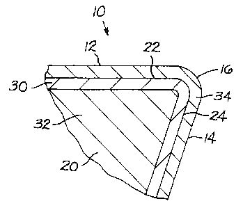
Referring to the drawings, FIG. 1 illustrates
a specific embodiment of the cutting insert of the
invention, generally designated as 10. Cutting
insert 10 includes a rake face 12 and a flank face 14
which intersect to form cutting edges 16. Cutting
insert l0 further has a bottom surface 18.
CA 02348851 2001-04-30
WO 00/31314 PCT/US99/25273
-9-
Referring to FIG. 2, cutting insert 10 has a
substrate 20 which has a substrate rake surface 22 and
a substrate flank surface 24. The substrate 20 also has
an exterior region 30 and an interior region 32. The
exterior region 30 defines the surfaces (22 and 24) of
the substrate 20. The exterior region 30 may extend
inwardly from the surfaces (22 and 24) of the substrate
a distance between about 1 micrometer and about 50
micrometers. There is a diamond coating 34 on the
substrate rake surface 22 and the substrate flank
surface 24 of the substrate 20. The diamond coating 34
has a thickness that may be between about 4 micrometers
and about 50 micrometers.
The typical substrate material is a tungsten
carbide-cobalt alloy with the possibility that there
are some additions of other elements such as, for
example, tantalum, titanium, niobium, chromium, hafnium
and vanadium. These other elements are typically in the
form of their simple carbides and/or in solid solution
with the tungsten carbide. The cobalt content can range
from between about 0.2 weight percent to about 20
weight percent. Two preferred substrate materials
comprise grades designated herein as Composition No. Z
and Composition No. 2 in the Table I set forth herein.
CA 02348851 2001-04-30
WO 00/31314 PCT/US99/25273
-10-
Table I
Composition and Properties of Compositions Nos. 1 and 2
.._.._ _-__-
Composition/
Property Comp. No. 1 Comp. No. 2
Cobalt (wt.%) 2.3-2.9 5.7-6.3
Tantalum (wt.%) up to 0.4 up to 0.1
Titanium (wt.%) up to 0.1 up to 0.1
Niobium (wt.%) up to 0.1 up to 0.1
Other (wt.%) --- Cr= 0.3-0.5
Tungsten & Carbon
(wt.%) Balance Balance
Hardness (Ra) 92.8-93.6 92.6-93.4
Coercive Force
(H ) Oersteds 290-440 250-320
Specific Gravity
(grams/cm3) 15.10-15.50 14.80-15.00
Grain Size (WC)
(micrometers] 1-6 1-5
Referring to Table I, the compositions are in weight
percent, the hardness is in Rockwell (Ra), the coercive
force is in oersteds, the specific gravity is in grams
per cubic centimeter, and the tungsten carbide grain
size is in micrometers (~Cm). The balance of each one of
the compositions is tungsten and carbon with most of
the tungsten and carbon in the form of tungsten
carbide.
In order to demonstrate the attributes of the
invention, examples were prepared for testing and
analysis. In regard to the processing of the examples,
typical powder metallurgical techniques were used to
prepare the green compacts. More specifically, the
powder components were ball milled and then consolidated
(e. g., pill pressing) into a partially dense so-called
green compact for subsequent heat treatments. The green
compacts are subsequently sintered and used as molded
inserts or ground to size. In the examples set forth in
this patent application fully sintered and ground
CA 02348851 2001-04-30
WO 00/31314 PCTlUS99/25273
-11-
cutting inserts (style SPG422) were heat treated;
however, it should be appreciated that molded cutting
inserts could have been heat treated in a similar
fashion.
Table II herein sets forth the steps which
comprised each one of the heat treatments wherein "T"
represents the temperature in °C, "P" represents the
pressure in Torr, and "t" represents the time of
duration in hours. More specifically, Process No. 1 and
l0 Process No. 2 comprise three steps each, and Process
No. 3 comprises four steps. Generally speaking, in each
one of these processes it is believed that the
formation of eta phase occurs when the cutting insert
substrate reaches a temperature of about 800°C so that
I5 one can say that eta phase occurs at the low
temperature oxidation of the substrate. Eta phase
means a double carbide phase which is due to a
deficiency in carbon. See pages 951-952 of Santhanam
et al., "Cemented Carbides," Metals Handbook, Vol. 2,
20 10th Edition (1990), pages 951-977. Eta phase is shown
by the article by Uhrenius, B., entitled "Phase
diagrams as a tool for production and development of
cemented carbides and steels," Powder Metallurgy,
(1992), Vol. 35, No. 3, pages 203-210, including
25 FIGS. 2a and 2b for the Co-W-C system. The Santhanam
et al. article and the Uhrenius article are hereby
incorporated by reference herein. Eta phase includes
W3Co3C, W6Co6C, W2Co4C and W3Co9C. Then, as the
cutting insert substrate with eta phase at the surface
30 reaches a temperature in the range of between 1250°C
and 2000°C, the eta phase converts to fibrous tungsten
carbide grains. The cobalt which exists due to the
conversion of the eta phase most likely evaporates from
the substrate, but there is a likelihood that some of
35 the cobalt will combine with tungsten and carbon to
form eta phase. Because of the difference in volume
between the eta phase and the fibrous tungsten carbide
CA 02348851 2001-04-30
WO 00/31314 PCT/US99/25273
-12-
grains, the conversion of the eta phase to the fibrous
tungsten carbide grains provides for the substrate
surface roughness that enhances the adhesion of the
diamond coating to the substrate.
Table II
Steps of the Heat Treatments
Process Process Process Process
No./Parameters No. 1 No. 2 No. 3
T1 [oC] ___ ___ 500
P1 [torr] --- --- vacuum
tl [hours] --- --- 1.0
T2 [C] 150 150 150
P2 [torr] vacuum vacuum 0.5 torr
nitrogen
t2 [hours] 2.0 2.0 2.0
T3 [C] 1450 1310 1310
P3 [torr] vacuum vacuum 0.5 torr
nitrogen
t3 [hours] 1.0 2.0 2.0
T4 [C] 2450 1310 1310
P4 [torr] vacuum vacuum vacuum
t4 [hours] 2.0 3.0 4.0
Although the above three processes each
provides for the formation of eta phase and the
subsequent conversion of the eta phase to fibrous
tungsten carbide grains, applicants contemplate the
invention to include a process (and the resultant
product) wherein the substrate with eta phase already
at the surface is heat treated (e.g., sintered in
vacuum) at a temperature in the range of between about
1250°C and about 2000°C in vacuum so as to convert the
eta phase to fibrous tungsten carbide grains with the
cobalt from the conversion of the eta phase most
likely being evaporated from the surface of
CA 02348851 2001-04-30
WO 00/31314 PCT/US99/25273
-13-
the substrate. One example of such a process comprises
a substrate that has been subjected to an atmosphere of
hydrogen and carbon dioxide at about 1000°C so as to
form eta phase on the surface. Another example of such
a process comprises a substrate processed according to
the disclosure of U.S. Patent No. 5,585,176 to Grab et
al. which is then surface oxidized so as to produce eta
phase at the surface. Still another example of such a
process comprises a substrate which is decarburized at
the surface so that when heated above 800°C it will
form eta phase at the surface.
Table III sets forth the composition and
processing procedure for each one of the Examples
Nos. 1 through 6 which were subjected to the cutting
tests.
TalZ,l a I I I
Composition and Processing for Example Nos. 1 - 6
Processing Procedure
Example No. Composition No. (i.e., Process No.)
1 1 1
2 1 2
3 1 1
4 1 2
5 2 3
6 1 3
All of the Examples Nos. 1 through 6 were
coated with a diamond coating. In regard to Examples
Nos. 1 and 2, the process was according to a CVD
(chemical vapor deposition) hot filament technique in a
mixture of 1% methane and 99% hydrogen, at 10 torr
total gas pressure, and at a substrate temperature of
between about 775°C to 850°C. Other techniques such as
DC plasma jet or microwave plasma are also suitable
techniques for the deposition of the diamond coating.
CA 02348851 2001-04-30
WO 00/31314 PCT/US99/25273
-14-
In the coating process, it is preferred that the
temperature of the substrate during the coating
operation be maintained between about 700°C and about
875°C, and more preferable that the substrate
temperature range between 750°C and 850°C. In regard to
Examples Nos. 3 through 6, the substrates were coated
by an arc jet process which typically occurs at a
substrate temperature range of between about 700°C and
about 1000°C.
Table IV herein sets for the cutting test
results for examples of the invention (i.e., Examples
Nos. 1-6) as compared to conventional cutting inserts
with a diamond coating. In regard to the cutting
conditions, the cutting insert was a SPG422 style of
cutting insert with a 15° lead angle, the speed was
2500 surface feet per minute (sfm) [762 surface meters
per minute], the feed was 0.005 inches per revolution
(ipr) [0.127 millimeters per revolution], the depth of
cut was 0.025 inches [0.635 millimeters], and the
cutting insert and workpiece were flooded with coolant.
The workpiece material was an aluminum silicon alloy
grade designated as A390 Aluminum with a nominal 17~
silicon by weight.
The conventional cutting inserts are shown by
the designations Convent. 1 through Convent. 4. The
first conventional cutting insert (i.e., Convent. 1)
was a commercial PCD cutting insert sold by Kennametal
Inc. of Latrobe, Pennsylvania USA under the designation
KD100. The second, third and fourth conventional
cutting inserts, i.e., Convent. 2 through Convent. 4,
were commercial diamond coated cutting inserts sold by
Kennametal Inc. under the designation KCD25 and
prepared in the same diamond coating heat as Example
Nos. 1 and 2. The Kennametal KCD25 cutting inserts were
made according to the disclosure of U.S. Patent
No. 5,585,176 to Grab et al. entitled DIAMOND COATED
CA 02348851 2001-04-30
WO 00/31314 PC'T/US99/25273
-15-
TOOLS AND WEAR PARTS (which is hereby incorporated by
reference herein).
Table IV
Results of Cuttina Tests of Aluminum Silicon Alloy A390
Average Range
of
Thickness WorkpieceComments
Surface Weight of Surface About
of
Example/ RoughnessDiamondDiamond RoughnessMode
of
Properties(R,) CoatingCoating Tool (R,) Tool
[micro- Life
& Resultsinches] (mg) (pm) (minutes)[p-inches)Failure
1 [HF AW SE
086 at
RTOI 19 75 25.98 37.0 18.23 56-106 20 min.
A
2 [HF AW SE
086 at
RT25 23 18 24.08 36.1 16.13 32-83 18 min.
E
3 [arc AW SE
jet at
RT07 19 70 --- 17.1 4.00 39-6I 2 min.
A
4 [arc AW SE
jet at
RT21 23 20 --- 18.4 8.00 3I-77 4 min.
E
[arc AW SE
jet at
GW31 26 42 --- 14-20 4.00 38-100 4 min.
H
AW (0.0073
6 [arc inches)
jet SE at
RT32 26 12 --- t4-20 4.00 38-51 4 min.
H
Convent.
1
KD100 NA NA NA 20.00 30-66 AW
Convent.
2
[HF 086 AW SE
at
FQ65 >42 20.7 33.8 14.00 43-97 20 min.
Convent.
3
[HF 086
F G2 >42 25.9 36.0 10.91 35-68 AW
Convent.
4
[HF 086 AW SE
at
FQ659] >42 39.2 47.8 19.33 43-49 24 min.
5 In Table IV the surface roughness, Ra, of the coated
cutting insert is given in microinches (~.-inches), the
weight of the diamond coating deposited on the cutting
insert is given in milligrams (mg), and the average
thickness of the diamond coating is given in
micrometers (~.m). The tool life represents the amount
of time it took to develop 0.010 inch maximum flank
wear. The range of the surface roughness for the
workpiece after cutting is given in microinches. In the
CA 02348851 2001-04-30
WO 00/31314 PCT/US99/25273
-16-
Comments in Table IV, the designation "AW" means that
the diamond coating wore by abrasive wear, and the
designation "SE" refers to the amount of time (in
minutes) it took to wear through the diamond coating
and expose the substrate.
Referring to the results set forth in
Table IV above, all of the diamond coated cutting
inserts with surface eta phase tailed by abrasive wear
with no flaking detected through optical microscopy at
20X magnification. The wear rates of the diamond
coated cutting inserts with surface eta phase are in
accordance with known correlation between thickness and
performance wherein this correlation is the result of
the inventors' experience with metal cutting tests on
A390 aluminum in the Kennametal Metal Cutting
Laboratory. Examples Nos. 1 and 2 with diamond coating
thickness of 30 ~Cm or greater had wear resistances
comparable to the Kennametal KCD25 cutting insert.
Examples Nos. 1 and 2 also had wear resistances of at
least 805 of that of the Kennametal KDI00 PCD cutting
insert. Examples Nos. 3 through 6 had abrasive wear in
accordance with the known correlation between diamond
coating thickness and performance. In this regard, the
average thickness of the diamond coating of Examples
Nos. 3 through 6 ranged between 14 ~Cm and 20 Vim. These
thicknesses were less than the average thickness of the
conventional cutting inserts which ranged between about
3 3 ~.m and about 4 8 ~,m .
A milling test with a single tooth flycutter
was performed with the inserts at 3500 sfm [1066.8
surface meters per minute], 0.004 ipt [.0102
centimeters per tooth], and 0.040 inch [0.1016
centimeters] DOC. The workpiece materials were 383.2
aluminum silicon alloy with 11~ silicon and A390
aluminum silicon alloy with 17~ silicon. Some
properties of the cutting inserts and the test results
are set forth in Table V below.
CA 02348851 2001-04-30
WO 00/31314 PCT/US99/25273
-17-
Table V
Results of Milling Tests
Results
of
!, Milling
of
the
A390
Average Alloy
Example Surface DiamondDiamond Results (number
of
No./ RoughnessCoatingCoating Milling of Comments
of
Properties(R, p- Weight Thicknessthe 3$3.2passes about
to the
& Resultsinches) (mg) (microns)Alloy failure)Test
Convent. NM NM NM 31.00 0.0073
1 inch
wearland
after
31.00
asses
Convent.2>42 20.7 33.8 NF 17.00 -
1 75 26.0 37.0 NF 17.00 -
2 18 24.1 36.1 NF FL 4 passes
in
A390
generated
flakin
3 70 9.5 17.1 NF FL 2 passes
in
A390
generated
flakin
4 20 10.3 18.4 NF FL 1 pass
in
A390
generated
flakin
42 9.5 NM FL FL 1 pass
in
A390
generated
flakin
6 12 10.2 NM FL NT
In Table V above, the surface roughness, Ra, of the
coated cutting insert is given in microinches
5 (~.-inches), the weight of the diamond coating deposited
on the cutting insert is given in milligrams (mg), and
the average thickness of the diamond coating is given
in micrometers. The tool life represents the amount of
time it took to develop 0.010 inch maximum flank wear.
The range of the surface roughness for the workpiece
after cutting in given in microinches. In regard to the
results of the milling of the 383.2 aluminum silicon
CA 02348851 2001-04-30
WO 00/31314 PCT/US99125273
-18-
alloy, three sets of four passes were performed to
check for flaking of the coating because wear patterns
took a long time to develop in the 383.2 aluminum
silicon alloy. In regard to the results of the milling
of the A390 alloy, the failure criterion in the A390
aluminum silicon alloy was severe flaking of the
coating or the number of passes for a 0.010 inch
wearland to develop. In Table V, the designation "NT"
means not tested, the designation "NM" means not
measured, the designation "NF" means no flaking, the
designation "FL" means flaking.
Only Examples Nos. 5 and 6 flaked in the
milling of the 383.2 aluminum silicon alloy. Example
No. 6 flaked due to a surface roughness that was much
too low for milling or severe interrupted cutting
according to U.S. Patent 5,585,176 at Col. 9, lines 40
through 42 and the inventors' experience with
interrupted cutting tests on A390 aluminum and 383.2
aluminum in the Kennametal Metal Cutting Laboratory.
Example No. 5 showed localized flaking; however, this
flaking did not prevent testing this cutting insert in
the milling of the A390 aluminum silicon alloy. In the
milling of the A390 aluminum silicon alloy, only the
Kennametal diamond coated insert with coating thickness
of 30 ~.m or greater and surface roughness greater than
or equal to 40 microinches Ra performed equally or
better than the Kennametal KCD25 cutting insert. This
performance is in agreement with known correlation for
milling A390 aluminum silicon alloy as set forth in
U.S. Patent 5,585,176 at Columns 9 and 10 and the
inventors' experience with interrupted cutting tests on
A390 aluminum and 383.2 aluminum in the Kennametal
Metal Cutting Laboratory.
Table VI below sets forth the features of
each one of FIGS. 3 through 29.
CA 02348851 2001-04-30
WO 00/31314 PCT/US99/25273
-I9-
Table VI
Features of FIGS. 3-29
Comments
on
Relation Presence
(if of
Composition any) to Eta Phase
at
(No.) & Coating Examples Substrate
of
FIG.Nature of Process (Technique)Table Surface
FIG. (No.) III
3 XRD Comp. 1 hot filamentEx. 2 eta phase
&
Proc. 2 resent
4 XItD Comp. 1 arc jet Ex. 4 eta phase
&
Proc. 2 resent
5 XRD Comp. 1 arc jet Ex. 6 eta phase
&
Proc. 3 resent
6 XRD Comp. 1 uncoated None eta phase
&
Proc. 2 resent
7 XRD Comp. 1 uncoated None eta phase
&
Proc. 1 resent
8 XltD Comp. 1 hot filamentEx. 1 eta phase
&
Proc. 1 resent
9 XRD Comp. 1 arc jet Ex. 3 eta phase
&
Proc. 1 resent
10 XRD - - Convent.2-
11 SEM of edgeComp. 2 uncoated None eta phase
&
surface Proc. 2 present
at at the
1000X ed a surface
12 SEM of edgeComp. 2 uncoated None eta phase
&
surface Proc. 2 present
at at the
SOOOX ed a surface
13 SEM of edgeComp. 2 uncoated None eta phase
&
surface Proc. 2 present
at at the
10,000X ed a surface
14 EDS of the Comp. 2 uncoated None eta phase
&
edge surfaceProc. 2 present
at the
ed a surface
15 SEM of centerComp. 2 uncoated None eta phase
&
surface Proc. 2 absent
at from
10,000X the center
surface
16 EDS of centerComp. 2 uncoated None eta phase
&
surface Proc. 2 absent
from
the center
surface
17 SEM of edgeComp. 1 uncoated None eta phase
&
surface Proc. 2 present
at at the
SOOOX ed a surface
18 EDS at the Comp. 1 uncoated None eta phase
&
edge surfaceProc. 2 present
at the
ed a surface
CA 02348851 2001-04-30
WO 00/31314 PCT/US99/25273
-20-
19 SEM of edgeComp. 1 uncoated None era phase
&
surface Proc. 2 present
at at the
7300X ed a surface
20 Spot EDS Comp. 1 uncoated Nane era phase
of &
edge surfaceProc. 2 present
at the
FIG. 19 ed a surface
21 Spot EDS Comp. 1 uncoated None era phase
of &
edge surfaceProc. 2 present
at the
FIG. 19 ed a surface
22 SEM of centerComp. 1 uncoated None era phase
&
surface Proc. 2 present
at at the
SOOOX center surface
23 EDS of the Comp. 1 uncoated None era phase
&
center surfaceProc. 2 present
at the
center surface
24 SEM of edgeComp. 1 uncoated None era phase
&
surface Proc. 1 present
at at the
1000X ed a surface
25 SEM of edgeComp. 1 uncoated None era phase
&
surface Proc. 1 present
at at the
5000X ed a surface
26 EDS of edgeComp. 1 uncoated None era phase
&
surface Proc. 1 present
at the
ed a surface
27 SEM of centerComp. I uncoated None era phase
&
surface Proc. 1 present
at at the
1000X center surface
28 SEM of centerComp. 1 uncoated None era phase
&
surface Proc. 1 present
at at the
SOOOX center surface
29 EDS of centerComp. 1 uncoated None era phase
&
surface Proc. 1 present
atthe
center surface
Now referring to FIGS. 3 through 9, overall,
the XRD analyses presented in FIGS. 3-9 show that era
phase existed on the surface of the substrates (of
Composition No. 1 with 2.3-2.9 wt.~ cobalt) after the
heat treatment pursuant to any one of Processes
Nos. 1-3 and before the application of the diamond
coating. Eta phase was also present after the
application of the diamond coating. The presence of era
phase after the application of the diamond coating
shows that the application of the diamond coating did
not decompose the era phase. The presence of era phase
after the application of the diamond coating also shows
that the cobalt in the era phase did not react with
CA 02348851 2001-04-30
WO 00/31314 PCT/US99/25273
-21-
the diamond. As is known in the art, the reaction of
cobalt with diamond is an undesirable occurrence. The
results set forth in FIGS. 3 through 9 are discussed in
detail hereinafter.
FIG. 3 reveals that eta phase was present on
the top face of a diamond coated cutting insert of
Composition No. 1 (see Table T) which was processed
according to Process No. 2 (see Table II). This cutting
insert was like Example No. 2 in Table IV.
FIG. 4 reveals that eta phase still existed
at the surface of the substrate after the arc jet
application of a diamond coating to the substrate of
Composition No. 1 processed according to Process No. 2.
This cutting insert of FIG. 4 was like Example No. 4 in
Table IV. FIG. 5 reveals the same basic condition on
the surface of this cutting insert as at the surface of
the cutting insert of FIG. 4 in that eta phase existed
on the substrate surface. The sample shown by FIG. 5 is
a cutting insert of Composition No. 1 processed
according to Process No. 3 after the arc jet
application of a diamond coating to the substrate. This
cutting insert of FIG. 5 is like Example No. 6 in
Table IV.
FIG. 6 reveals that eta phase existed at the
surface before the application of a diamond coating to
a substrate of Composition No. 1 which was processed
according to Process No. 2. Diamond coated cutting
inserts wherein the substrates were of Composition
No. 1 processed according to Process No. 2 are the
subject of FIG. 3 (hot filament technique) and FIG. 4
(arc jet technique). FIGS. 3 and 4 show that for each
diamond application technique, eta phase existed at the
surface of the substrate. It thus becomes apparent that
the application of the diamond coating (via either the
hot filament technique or the arc jet technique) did
not decompose the eta phase at the surface. The
presence of eta phase after the application of the
CA 02348851 2001-04-30
WO 00/31314 PCT/US99/25273
-22-
diamond coating also reveals that the cobalt in the eta
phase did not react with the diamond applied by either
the hot filament technique or the arc jet technique.
FIG. 7 shows that eta phase existed at the
surface of an uncoated substrate of Composition No. 1
which was processed according to Process No. 1. FIG. 8
reveals that eta phase was present on the top face of a
sample of Composition No. 1 after the application of a
diamond coating by the hot filament technique to the
to substrate processed according to Process No. 1. The
diamond coated cutting insert of FIG. 8 is like Example
No. 1 in Table IV. A slow scan of the XRD spectrum
enhances the intensity of the eta phase peaks. FIG. 9
reveals that eta phase was present on the top face of a
sample of Composition No. 1 after the application of a
diamond coating by the arc jet method to the substrate
processed according to Process No. 1. The diamond
coated cutting insert of FIG. 9 is like Example No. 3
in Table IV. A comparison of the results set out in
FIGS. 7 through 9 show that the application of a
diamond coating, by either the hot filament technique
or the arc jet method, did not decompose the eta phase.
Such a comparison of FIGS. 7-9 also shows that the
cobalt in the eta phase did not react with the diamond.
FIG. 10 shows the XRD spectrum of a diamond
coated cutting insert prepared according to U.S. Patent
No. 5,585,176 to Grab et al. This cutting insert is
like Convent. No. 2 in Table IV.
The results of SEM analysis and EDS analysis
of a number of uncoated cutting insert substrates are
set forth in FIGS. 11 through 29. A detailed discussion
of the results presented by FIGS. 11-29 now follows.
FIGS. 11 through 13 are photomicrographs at
different magnifications taken via scanning electron
microscopy (SEM). These photomicrographs (FIGS. 11-13)
show the surface of the edge of a substrate of
Composition No. 2 processed according to Process No. 2.
CA 02348851 2001-04-30
WO 00/31314 PCT/US99/25273
-23-
These photomicrographs show the presence of eta phase
along the edge of the cutting insert. FIGS. 12 and 13
show the presence of fibrous tungsten carbide grains at
the surface of the edge of the substrate. These fibrous
tungsten carbide grains are the result of the partial
conversion of the eta phase to tungsten carbide grains
and the evaporation of cobalt, which was present from
the conversion of the eta phase, during the heat
treatment (i.e., sintering). Such fibrous tungsten
carbide grain growth provides for an irregular surface
due to a difference in the volume between the eta phase
and the fibrous tungsten carbide grains. The presence
of the irregular surface enhances the surface roughness
of the substrate. Surface prafilometer measurements
along the edge gave a surface roughness of 45
microinches Ra, for the cutting insert of FIGS. 11-13.
FIG. 14 shows the results of an EDS analysis
of the surface of the edge of the cutting insert
substrate (Composition No. 2/ Process No. 2) shown in
FIGS. 11 through 13. It is typical in a cobalt cemented
tungsten carbide that the cobalt is located at the
interstices of the tungsten carbide grains. The EDS
analysis in FIG. 14 reveals, however, that the surface
at the edge of the insert was atypical of cobalt
cemented tungsten carbide. Subsequent analysis of the
edge and the corner areas of this cutting insert with
Murakami's reagent, a standard laboratory practice for
the detection of eta phase, showed there to be eta
phase due to the rapid etching of this phase in
Murakami's reagent. It should be appreciated that the
location of the eta phase at the corners and edges of
the cutting insert prevented the focusing of the X-ray
beam on these areas and prevented the identification of
the eta phase type via the X-ray diffraction technique.
FIG. 15 shows an SEM photomicrograph of the
center of the cutting insert (Composition No. 2/
Process No. 2) whose edges are shown in FIGS. 11
CA 02348851 2001-04-30
WO 00/31314 PCT/US99125273
-24-
through 13. FIG. 16 is an EDS analysis of the surface
of the same center area shown in FIG. 15. The
photomicrograph of FIG. 15 and the EDS scan of FIG. 16
reveal that eta phase was absent from the surface of
the center of the cutting insert substrate. Subsequent
scans by SEM over the surface confirmed that eta phase
was present only at the edges and corners of the
cutting insert, and that eta phase was absent from the
center of the cutting insert. The center of the cutting
insert (Composition No. 2/ Process No. 2) shown in
FIG. 15 presents a microstructure like that of samples
produced according to U.S. Patent No. 5,585,176 to Grab
et al.
Referring to the good adhesion properties of
the diamond coating to a cutting insert substrate like
that shown in FIGS. 11-16 (Composition No. 2/ Process
No. 2), there should be good adhesion of the diamond
coating at the center of the cutting insert due to the
surface roughness (even in the absence of eta phase)
since the surface at the center is like that disclosed
in U.S. Patent No. 5,585,176 to Grab et al., which
discusses the adhesion of a diamond coating due to
surface roughness. There should be good adhesion of the
diamond coating at the edges and corners of the cutting
insert substrate due to the presence of the fibrous
tungsten carbide grains which presented an acceptable
surface roughness. It can thus be seen that there
should be good adhesion of the diamond coating to the
center, as well as the edges and corners, of the
cutting insert substrate.
FIG. 17 shows an SEM photomicrograph at 5000X
magnification of the surface of the edge of a cutting
insert (Composition No. 1/ Process No. 2). FIG. 18
shows an EDS spectrum of the same sample area as shown
in FIG. 17, but at 1000X magnification. The EDS
spectrum of FIG. 18 shows large peaks due to cobalt.
FIG. 19 shows an SEM photomicrograph at 7300X
CA 02348851 2001-04-30
WO 00/31314 PCT/US99l25273
-25-
magnification of the same area shown in FIG. 17. In
FIG. 19 the box which corresponds with Arrow A shows
the location (i.e., the area defined by the box) of the
spot EDS analysis shown in FIGS. 20. In FIG. 19 the box
which corresponds with Arrow B shows the location
(i.e., the area defined by the box) of the spot EDS
analysis shown in FIG. 21. FIGS. 17 and 19 show the
microstructures that are eta phase, as well as the
microstructures that are fibrous tungsten carbide
grains. As mentioned. above, the fibrous tungsten
carbide grains were the result of the partial
conversion of the eta phase into tungsten carbide and
the evaporation of the cobalt, which was present from
the conversion of the eta phase, from the surface of
the substrate during the sintering at vacuum within the
temperature range of 1250°C and 2000°C. Similar
microstructures (i.e., eta phase and fibrous tungsten
carbide grains) are observed at the center of the
insert shown in FIG. 17.
FIG 22 is an SEM photomicrograph at 5000X
magnification of the surface of the center of the
cutting insert shown in FIG. 17. FIG. 23 is an EDS
spectrum of the surface area (i.e., center) shown in
FIG. 22. The SEM and EDS results set forth in FIGS. 22
and 23, and when coupled with the XRD results of the
same cutting insert as shown in FIG. 6, show that the
structure of the surface is composed largely of eta
phase with fibrous tungsten carbide grains growing from
the eta phase as described above. The growth of the
fibrous tungsten carbide grains enhance (i.e.,
increase) the surface roughness, which provides for the
enhanced adhesion of the diamond coating to the cutting
insert substrate.
It is apparent that there is a distinction in
the microstructure at the surface of the cutting insert
of FIGS. 11-16 and the cutting insert of FIGS. 17-23.
This distinction is the absence of eta phase and
CA 02348851 2001-04-30
WO 00/31314 PCT/US99/25273
-26-
fibrous tungsten carbide grains from the center surface
of the cutting insert substrate of FIGS. 11-16 in
contrast to the presence of eta phase and fibrous
tungsten carbide grains at the center surface of the
cutting insert substrate of FIGS. 17-23. Both cutting
insert substrates had eta phase and fibrous tungsten
carbide grains at the corner and edge surfaces.
Applicants believe that reasons exist which
explain the difference in the microstructure between
the cutting insert substrate of FIGS. 11-16 and the
cutting insert substrate of FIGS. 17-23. These reasons
pertain to the difference in the cobalt content of the
cutting insert substrates and the difference in the
mass of the cutting insert substrate adjacent the
center and adjacent the edges and corners thereof.
The cutting insert substrate of FIGS. 11-16
had a greater cobalt content (i.e., 5.7-6.3 wt.~) than
the cutting insert substrate of FIGS. 17-23 (i.e.,
2.3-2.9 wt.~). For the higher cobalt cutting insert
substrate of FIGS. 11-16, there was more carbon
available for migration during the heat treatment to
correct the carbon deficiency due to the presence of
the eta phase. For the lower cobalt cutting insert
substrate of FIGS. 17-23, there was little, if any,
carbon available to correct the carbon deficient due to
the presence of eta phase. Thus, there was the tendency
in the higher cobalt cutting insert substrate to
correct the eta phase while in the lower cobalt cutting
insert such a tendency was slight, if at all. There was
more mass of material adjacent to the center surface of
the cutting insert substrate than was adjacent to the
edges (and corners) of the cutting insert substrate.
Thus, the migration of carbon, to the extent it
occurred, was more vigorous adjacent to the center
surface of the cutting insert substrate than at the
edges of the cutting insert substrate.
CA 02348851 2001-04-30
WO 00/31314 PCT/US99/25273
-27-
These reasons reveal that the more vigorous
migration of carbon at the center section of the higher
cobalt cutting insert substrate resulted in the
correction of eta phase, and hence, the absence of eta
phase at the center surface. The absence of any eta
phase would, of course, result in the absence of
fibrous tungsten carbide grains due to the conversion
of eta phase.
Because of the less vigorous migration of
carbon at the edges, the edge and corner surfaces of
the higher cobalt cutting insert substrate had eta
phase and fibrous tungsten carbide grains, due to the
partial conversion of the eta phase, present thereat.
The absence of carbon to correct the eta phase in the
lower cobalt cutting insert substrate resulted in the
presence of eta phase and fibrous tungsten carbide
grains, due to the partial conversion of the eta phase,
at both the center surface and at the edge and corner
surfaces .
FIGS. 24 and 25 show SEM photomicrographs at
different magnifications taken at the surface of the
edge of a substrate of Composition No. 1 which was
processed according to Process No. 1. FIG 26 shows an
EDS spectrum of the surface of the same area of the
substrate as shown in FIGS. 24 and 25. No cobalt was
observed in the EDS spectrum.
FIGS. 27 and 28 show SEM photomicrographs at
different magnifications of the surface at the center
of the same substrate shown in FIGS. 24 and 25. FIG. 29
shows an EDS spectrum of the surface of the same area
(i.e., center) shown in FIGS. 27 and 28, but at 200X
magnification. Once again no cobalt peak was observed
in the EDS spectrum. This is the same substrate for
which the XRD spectrum is shown in FIG. 7, and which
shows that M6C eta phase was present.
A comparison of FIGS. 24 and 25 with FIGS. 11
and 12 and FIGS. 17 and 19 shows microstructures that
CA 02348851 2001-04-30
WO 00/31314 PCT/US99/25273
-28-
look very much similar in that there existed eta phase
partially converted to fibrous tungsten carbide grains
along with cobalt evaporation. These figures (FIGS. 24,
25, 11, 12, 17 and 19) show that more eta phase was
converted to fibrous tungsten carbide grains in the
cutting insert substrate processed at the higher
temperature of 1450°C [Process No. 1 and FIGS, 24 and
25] as compared to the lower temperature of 1310°C
[Process No. 2 and FIGS. 11, 12, 17 and 19].
Similarly, a comparison of FIGS. 27 and 28
with FIG. 22 shows a similar result in that more eta
phase was converted into fibrous tungsten carbide
grains at the center of the substrate subjected to the
higher temperature of 1450°C (FIGS. 27 and 28) as
compared to the lower temperature of 1310°C. The
increase in the conversion of the eta phase to fibrous
tungsten carbide grains due to the higher temperatures
produced a substrate with excellent surface roughness
for good diamond coating adhesion. Furthermore, the
surface of the substrate was devoid of free cobalt due
to either the evaporation of cobalt and/or the
combining of the cobalt with tungsten and carbon as eta
phase. Since there was no free cobalt, there was no
cobalt to react with a diamond coating. Such a reaction
between diamond and cobalt is known to result in the
poor adhesion of the diamond film.
when a sample of Composition No. 1 was
processed according to Process No. 1, but the
temperatures T3 and T4 were 1500°C instead of 1450°C,
the XRD pattern taken on the top face of the cutting
insert substrate showed that WC, W2C, and M6C type eta
phase were present. The results of SEM and EDS analysis
of such a sample (Composition No. 1/ Process No. 1 at
T3 and T4 equal to 1500°C) were similar to those shown
in FIGS. 24 through 29 hereof in that the substrate had
eta phase and fibrous tungsten carbide grains which
CA 02348851 2001-04-30
WO 00/31314 PCT/US99/25273
-29-
resulted in a surface roughness adequate to provide
good adhesion of a diamond coating.
Another example of the invention comprised
making a fiberglass router in Composition No. 1. The
substrate was oxidized so as to form eta phase at the
surface, then sintered at 1510°C for three hours and
then coated with diamond by the arc jet technique.
FIG. 30 shows a photomicrograph of the surface of the
tip portion of the fiberglass router prior to the
application of the diamond coating.
FIG. 31 shows the results of the EDS analysis
of the surface at the tip portion of the fiberglass
router of FIG. 30. It is apparent that eta phase and
fibrous tungsten carbide grains were present at the
surface of the substrate. FIG. 32 shows a
photomicrograph of the surface of the center portion of
the fiberglass router prior to the application of the
diamond coating.
FIG. 33 shows the results of the EDS analysis
of the surface at the center portion. It is apparent
that eta phase with the fibrous tungsten carbide grain
growth is present at the surface of the substrate.
The fiberglass router was tested by machining
a carbon graphite panel used in an airplane wherein the
general shape of the panel was similar to the shape of
a very large automobile windshield having complex
compound curves. The machining operation required the
removal of excess ragged edges of the material to
produce a precisely dimensioned part. More
specifically, the removal was done by passing the 3/8th
inch (.952 cm) diameter fiberglass router through the
3/l6th inch (.476 cm) thick panel so as to traverse the
entire periphery of the part until the excess material
falls to the floor. The next step required feeding the
fiberglass router 0.050 inches (1.27 cm) inward to make
a finish pass on the periphery so as to arrive at the
final size and finish. The length of each pass was 12
CA 02348851 2001-04-30
WO 00/31314 PCT/US99/25273
-30-
feet (3.94 meters). The rough cut was made at 7000
revolutions per minute (rpm) and 60 inches per minute
(ipm) (152.4 centimeters per minute]. The finish cut
was made at 7000 rpm and 80 ipm (203.2 cm/minute).
In the past, an uncoated fiberglass router
which had been used to finish the previous part was
used to rough cut the next part. Then a new fiberglass
router was used to finish the rough-cut part. The
coated fiberglass router was able to rough cut and
finish cut the part.
It thus becomes apparent that the instant
invention provides for a diamond coated cutting insert
wherein the diamond coating is strongly adherent to the
surface of the substrate, the diamond coating may be
applied in sufficiently great thickness to provide for
sufficient tool life, and the surface roughness of the
workpiece is sufficiently smooth.
While the invention has been described in
detail with respect to diamond coated indexable cutting
inserts for metalcutting applications, it is not
limited to cutting inserts for metalcutting. The
present invention may be applied to round tools (e. g.,
drills, end mills, taps, reamers, burrs, routers,
thread mills and circular saws), and other cutting
inserts which may not be indexable. Cutting inserts in
accordance with the present invention may also be
suitable for the removal of material from workpieces
such as free-machining aluminum alloys, high silicon
aluminum, nonferrous materials (e. g., copper, bronze,
and brass), ceramics materials, fiber-reinforced
materials, graphite laminates, nylons, acrylics,
phenolic resin materials, metal matrix composites
(e. g., silicon carbide or alumina in an aluminum
matrix), plastic, rubber and wood. The present
invention may also have application as a wear part
(e. g., TAB bonders for electronic applications, dies,
and punches) and for cemented carbide tips used in mine
CA 02348851 2001-04-30
WO 00/31314 PCT/US99/25273
-31-
tools, construction tools, and drilling tools for earth
and rock.
The patents and other documents identified
herein are hereby incorporated by reference herein.
Other embodiments of the invention will be
apparent to those skilled in the art from a
consideration of the specification or practice'of the
invention disclosed herein. It is intended that the
specification and examples be considered as
l0 illustrative only, with the true scope and spirit of
the invention being indicated by the following claims.