Note : Les descriptions sont présentées dans la langue officielle dans laquelle elles ont été soumises.
CA 02348930 2001-04-23
= WO 00/29217 PCT/GB99/04
-1-
DROPLET DEPOSITION APPARATUS
-
The present invention relates to droplet deposition apparatus, particularly
inkjet printheads, components thereof and methods for manufacturing such
components.
A particularly useful form of inkjet printer comprises a body of piezoelectric
material with ink channels formed, for example, by disc cutting. Electrodes
can be
plated on the channel-facing surfaces of the piezoelectric material, enabling
an
electrical field to be applied to the piezoelectric "wall" defined between
adjacent
channels. With appropriate poling, this wall can be caused to move into or out
of the
selected ink channel, causing a pressure pulse which ejects an ink droplet
through
an appropriate channel nozzle. Such a construction is shown, for example, in
EP-A-0 364 136.
It is a frequent requirement to provide a high density of such ink channels,
with precise registration across a relatively large expanse of printhead,
perhaps an
entire page width. A construction that is useful to this end is disclosed in
WO 98/52763. It involves the use of a flat base plate that supports the
piezoelectric
material as well as integrated circuits performing the necessary processing
and
control functions.
Such a construction has several advantages, particularly with regard to
manufacture. The base plate acts as a "backbone" for the printhead, supporting
the
piezoelectric material and integrated circuits during manufacture. This
support
function is particulariy important during the process of butting together
multiple
sheets of piezoeiectric material to form a contiguous, pagewide array of ink
channels. The relatively large size of the base plate also simplifies
handling.
A problem remains of reliably and efficiently establishing electrical
connection
between the ink channel electrodes and the corresponding pins of the
integrated
circuits. If the base plate is of suitable material and suitably finished,
conductive
tracks can be deposited on it, these tracks connecting in known manner with
the IC
pins. There remains the difficulty of establishing connections to channel
electrodes.
CA 02348930 2001-04-23
=00/29217 PCT/GB99/03799 =
-2-
The present invention seeks to provide improved apparatus and methods
which address this problem.
Accordingly, the present invention consists in one aspect in a method of
manufacturing a component of a droplet deposition apparatus, the component
comprising a body of piezoelectric material having a plurality of channels
each with a
channel surface and a base, the body being attached to a surface of the base
which
is free of substantial discontinuities; the method comprising the steps of
attaching
the body to said surface of the base; and depositing a layer of conductive
material
so as to extend continuously over at least one of said channel surfaces and
said
surface of the base to provide an electrode on each channel surface and a
conductive track on said surface of the base which is integrally connected to
the
electrode.
The attachment of the body to a surface of the base and subsequent
deposition of a continuous layer of conductive material over said at least one
channel surface and the base surface results in an effective and reliable
electrical
connection between channel wall electrodes and substrate conductive tracks.
Those
tracks can be used to provide connection with one or more integrated circuits
carried
on the base, either directly or through other tracks and interconnections.
The present invention also consists in a component for a droplet deposition
apparatus comprising a body of piezoelectric material formed with a plurality
of
channels each channel having a channel surface; and a separate base having a
base surface free of substantial discontinuities; wherein the body is attached
to said
base surface and a layer of conductive material extends continuously over said
channel surfaces of and said base surface, thereby defining an electrode on
each
channel surface and a conductive track connected thereto on the base surface.
The invention will now be described by way of example with reference to the
accompanying drawings, in which:
Figure 1 is a longitudinal sectional view through a known ink jet printhead;
Figure 2 is a transverse sectional view on line AA of Figure 1
Figure 3 is an exploded view of a page wide printhead array according to the
prior art;
CA 02348930 2001-04-23
= WO 00/29217 PCT/GB99/009
-3-
Figure 4 is an assembled longitudinal sectional view through the printhead
shown in Figure 3;
Figure 5 is an assembled sectional view, similar to that of Figure 4, of a
printhead according to a first embodiment of the invention;
Figures 6(a) and 6(b) are detail sectional views taken perpendicular and
parallel to the channel axis of the device of Figure 5;
Figure 7 is a detail perspective view of the device of Figure 5;
Figure 8 is a cross-sectional view through a channel of a printhead according
to a second embodiment of the invention;
Figures 9-11 are a sectional views along the channel of third, fourth and
fifth
embodiments of the invention respectively;
Figures 12 and 13 are perspective and detail perspective views respectively
of the embodiment of Figure 11;
Figure 14 is a detail view of the area denoted by reference Figure 194 in
Figure 6(b);
Figure 15 is a perspective view showing a step in the manufacture of a
printhead of the kind shown in Figure 11; and
Figure 16 is a sectional view illustrating a further modification.
It will be helpful to describe first in some detail, examples of the prior art
constructions referred to briefly above.
Thus, Figure 1 shows a prior art inkjet printhead I of the kind disclosed in
WO 91/17051 and comprising a sheet 3 of piezoelectric material, for example
lead
zirconium titanate (PZT), formed in a top surface thereof with an array of
open-
topped ink channels 7. As evident from Figure 2, which is a sectional view
taken
aiong line AA of Figure 1, successive channels in the array are separated by
side
walls 13 which comprise piezoelectric material poled in the thickness
direction of the
sheet 3 (as indicated by arrow P). On opposite channel-facing surfaces 17 are
arranged electrodes 15 to which voltages can be applied via connections 34. As
is
known, e.g. from EP-A-0 364 136, application of an electric field between the
CA 02348930 2007-06-01
-4-
electrodes on either side of a wall results in shear mode deflection of the
wall into
one of the flanking channels - this is shown exaggerated by dashed lines in
Figure 2 - which in turn generates a pressure pulse in that channel.
The channels are closed by a cover 25 in which are formed nozzles 27
each communicating with respective channels at the mid-points thereof. Droplet
ejection from the nozzles takes place in response to the aforementioned
pressure
pulse, as is well known in the art. Supply of droplet fluid into the channels,
indicated by arrows S in Figure 2, is via two ducts 33 cut into the bottom
face 35 of
sheet 3 to a depth such that they communicate with opposite ends respectively
of
1o the channels 7. Such a channel construction may consequently be described a
double-ended side-shooter arrangement. A cover plate 37 is bonded to the
bottom
face 35 to close the ducts.
Figures 3 and 4 are exploded perspective and sectional views respectively of a
printhead employing the double-ended side-shooter concept of Figures 1 and 2
in
a "pagewide" configuration. Such a printhead is described in WO 98/52763. Two
rows of channels spaced relatively to one another in the media feed direction
are
used, with each row extending the width of a page in a direction 'W'
transverse to
a media feed direction P. Features common with the embodiment of Figures 1 and
2 are indicated by the same reference Figures used in Figures 1 and 2.
2o As shown in Figure 4, which is a sectional view taken perpendicular to the
direction W, two piezoelectric sheets 82a, 82b each having channels (formed in
their bottom surface rather than their top as in the previous example) and
electrodes as described above are closed (again on their bottom surface rather
than their top) by a flat, extended base 86 in which openings 96a, 96b for
droplet
ejection are formed. Base 86 is also formed with conductive tracks (not shown)
which are electrically connected to respective channel electrodes, e.g. by
solder
bonds as described in WO 92/22429, and which extend to the edge of the base
CA 02348930 2006-11-03
- 4(a) -
where respective drive circuitry (integrated circuits 84a, 84b) for each row
of
channels is located.
Such a construction has several advantages, particularly with regard to
manufacture. Firstly, the extended base 86 acts as a "backbone" for the
printhead,
CA 02348930 2001-04-23
= WO 00/29217 PCT/GB99/0%#9
-5-
supporting the piezoelectric sheets 82a,82b and integrated circuits 84a, 84b
during
manufacture. This support function is particularly important during the
process of
butting together multiple sheets 3 to form a single, contiguous, pagewide
array of
channels, as indicated at 82a and 82b in the perspective view of Figure 3. One
approach to butting is described in WO 91/17051 and consequently not in any
further
detail here. The size of the extended cover also simplifies handling.
Another advantage arises from the fact that the surface of the base on which
the conductive tracks are required to be formed is flat, i.e. it is free of
any substantial
discontinues. As such, it allows many of the manufacturing steps to be carried
out
using proven techniques used elsewhere in the electronics industry, e.g.
photolithographic patterning for the conductive tracks and "flip chip" for the
integrated circuits. Photolithographic patterning in particular is unsuitable
where a
surface undergoes rapid changes in angle due to problems associated with the
spinning method typically used to apply photolithographic films. Flat
substrates also
have advantages from the point of view of ease of processing, measuring,
accuracy
and availability.
A prime consideration when choosing the material for the base is, therefore,
whether it can easily be manufactured into a form where it has a surface free
of
substantial discontinuities. A second requirement is for the material to have
thermal
expansion characteristics to the piezoelectric material used elsewhere in the
printhead. A final requirement is that the material be sufficiently robust to
withstand
the various manufacturing processes. Aluminium nitride, alumina, INVAR or
special
glass AF45 are all suitable candidate materials.
The droplet ejection openings 96a, 96b may themselves be formed with a
taper, as per the embodiment of Figure 1, or the tapered shape may be formed
in a
nozzle plate 98 mounted over the opening. Such a nozzle plate may comprise any
of the readily-ablatable materials such as polyimide, polycarbonate and
polyester
that are conventionally used for this purpose. Furthermore, nozzle manufacture
can
take place independently of the state of completeness of the rest of the
printhead:
the nozzle may be formed by ablation from the rear prior to assembly of the
active
body 82a onto the base or substrate 86 or from the front once the active body
is in
CA 02348930 2001-04-23
41O 00/29217 PCT/GB99/03799
-6-
place. Both techniques are known in the art. The former method has the
advantage
that the nozzle plate can be replaced or the entire assembly rejected at an
early
stage in assembly, minimising the value of rejected components. The latter
method
facilitates the registration of the nozzles with the channels of the body when
assembled on the substrate.
Following the mounting of piezoelectric sheets 82a, 82b and drive chips 84a,
84b onto the substrate 86 and suitable testing as described, for example, in
EP-A-0 376 606 - a body 80 can be attached. This too has several functions,
the
most important of which is to define, in cooperation with the base or
substrate 86,
manifold chambers 90,88 and 92 between and to either side of the two channel
rows
82a, 82b respectively. Body 80 is further formed with respective conduits as
indicated at 90', 88'and 92' through which ink is supplied from the outside of
the
printhead to each chamber. It will be evident that this results in a
particularly
compact construction in which ink can be circulated from common manifold 90,
through the channels in each of the bodies (for example to remove trapped dirt
or air
bubbles) and out through chambers 88 and 92. Body 80 also provides surfaces
for
attachment of means for locating the completed printhead in a printer and
defines
further chambers 94a, 94b, sealed from ink-containing chambers 88,90,92 and in
which integrated circuits 84a, 84b can be located.
Tuming now to an example of the present invention, reference is made to
Figure 5. This is a sectional view similar to that of Figure 4, illustrating a
printhead in
accordance with the present invention. Wherever features are common with the
embodiments of Figure 1-4, the same reference figures as used in Figures 1-4
have
been used.
As with the previous embodiments, the printhead of Figure 5 comprises a
"pagewide" base plate or substrate 86 on which two rows of integrated circuits
84
are mounted. In-between lies a row of channels 82 formed in the substrate 84,
each
channel of which communicates with two spaced nozzles 96a, 96b for droplet =
ejection and with manifolds 88, 92 and 90 arranged to either side and between
nozzles 96a, 96b respectively for ink supply and circulation.
CA 02348930 2001-04-23
WO 00/29217 PCT/GB99/09
-7-
In contrast to the printhead embodiments discussed above, the piezoelectric
material for the channel walls is incorporated in a layer 100 made up of two
strips
110a, 110b. As in the embodiment of Figure 4, these strips will be butted
together in
the page width direction W, each strip extending approximately 5-10 cm (this
being
the typical dimension of the wafer in which form such material is generally
supplied).
Prior to channel formation, each strip is bonded to the continuous planar
surface 120
of the substrate 86, following which channels are sawn or otherwise formed so
as to
extend through both strip and substrate. A cross-section through a channel,
its
associated actuator walls and nozzle is shown in Figure 6. Such an actuator
wall
construction is known, e.g. from EP-A-0 505 065 and consequently will not be
discussed in any greater detail. Similarly, appropriate techniques for
removing both
the glue bonds between adjacent butted strips of piezoelectric material and
the glue
relief channels used in the bond between each piezoelectric strip and the
substrate
are known from US 5,193,256 and WO 95/04658 respectively.
In accordance with the present invention, a continuous layer of conductive
material is then applied over the channel walls and substrate. Not only does
this
form electrodes 190 for application of electric fields to the piezoelectric
walls 13 - as
illustrated in Figure 6(a) - and conductive tracks 192 on substrate 86 for
supply of
voltages to those electrodes as shown in Figure 6(b) - it also forms an
electrical
connection between these two elements as shown at 194.
Appropriate electrode materials and deposition methods are well-known in the
art. Copper, Nickel and Gold, used alone or in combination and deposited
advantageously by electroless processes utilising palladium catalyst will
provide the
necessary integrity, adhesion to the piezoelectric material, resistance to
corrosion
and basis for subsequent passivation e.g. using Silicon Nitride as known in
the art.
As is generally known, e.g. from the aforementioned EP-A-0 364 136, the
electrodes on opposite sides of each actuator wall 13 must be electrically
isolated
from one another in order that an- electric field may be established between
them
and hence across the piezoelectric material of the actuator wall. This is
shown in
both the prior art arrangement of Figure 2 and the embodiment of the present
CA 02348930 2001-04-23
0600/29217 PCT/GB99/03799
-8-
invention shown in Figure 6(a). The corresponding conductive tracks connecting
each electrode with a respective voltage source must be similarly isolated.
In the present invention, such isolation may be achieved at the time of
deposition for example by masking those areas - such as the tops of the
channel
walls - where conductive material is not required. Suitable masking
techniques,
including patterned screens and photolithographically pattemed masking
materials
are well-known in the art, e.g. from WO 98/17477 and EP-A-0 397 441, and will
not
be described in any further detail.
Altematively, isolation may be achieved after deposition by removing
conductive material from those areas where it is not required. Localised
vaporisation of material by laser beam, as known e.g. from JP-A-09 010 983,
has
proved most suitable for achieving the high accuracy required, although other
conventional removal methods - inter alia sand blasting, etching,
electropolishing
and wire erosion may also be suitable. Figure 7 illustrates material removal,
in this
case over a narrow band running along the top of the wall, although several
passes
of the laser beam (or a single pass of a wider laser beam) can be used to
remove
material from the entire top surface of the wall so as to maximise the wall
top area
available for bonding with the cover member 130.
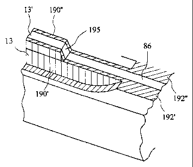
In addition to removing conductive material from the top surface 13' of each
piezoelectric actuator wall 13 so as to separate the electrodes 190', 190", on
either
side of each wall, conductive material must also be removed from the surface
of the
substrate 86 in such a way as to define respective conductive tracks 192',
192" for
each electrode 190' 190". At the transition between piezoelectric material 100
and
substrate 86, the end surface of the piezoelectric material 100 is angled or
chamfered as shown at 195. As is known, this has the advantage over a
perpendicular cut (of the kind indicated by a dashed line at 197) of allowing
the
vapourising laser beam - shown figuratively by arrow 196 - to impinge on and
thereby remove the conductive material without requiring angling of the beam.
Preferably, the chamfer 195 is formed by milling after the piezoelectric layer
100 has
been attached to the substrate 86 but before the formation of the channel
walls
CA 02348930 2001-04-23
= WO 00/29217 PCT/GB99/0IR9
-9-
which, being typically 3004m thick and formed of ceramic and glass, are
vulnerable
to damage. A chamfer angle of 45 degrees has been found to be suitable.
It will also be appreciated that the electrodes and conductive tracks
associated with the active portions 140a need to be isolated from those
associated
with 140b in order that the rows of nozzles might be operated independently.
Although this too may be achieved by a laser "cut" along the surface of the
substrate
86 extending between the two piezoelectric strips, it is more simply achieved
by the
use of a physical mask during the electrode deposition process or by the use
of
electric discharge machining.
Laser machining can also be used in a subsequent step to form the ink
ejection holes 96a, 96b in the base of each channel, as is known in the art.
Such
holes may directly serve as ink ejection nozzles. Alternatively, there may be
bonded
to the lower surface of the substrate 86 a separate plate (not shown) having
nozzles
that communicate with the holes 96a, 96b and which are of a higher quality
that
might otherwise be possible with nozzles formed directly in the ceramic or
glass
base of the channel. Appropriate techniques are well-known, particularly from
WO 93/15911 which discloses a technique for the formation of nozzles in situ,
after
attachment of the nozzle plate, thereby simplifying registration of each
nozzle with its
respective channel.
The conductive tracks 192', 192" defined by laser may extend all the way
from the transition area 195 to the integrated circuits 84 located at either
side of the
substrate. Alternatively, the laser track definition procegs may be restricted
to an
area directly adjacent the piezoelectric material and a different - e.g.
photolithographic - process used to define further conductive tracks that
connect the
laser-defined tracks with the integrated circuits 84.
Having established tile electrical connections, it remains only to adhesively
bond (e.g. using an offset method) a cover member 130 to the surface of
substrate
86. This cover fulfils several functions: firstly, it closes each channel
along those
portions 140a, 140b where the walls incorporate piezoelectric material in
order that
actuation of the material and the resulting deflection of the walls might
generate a
CA 02348930 2001-04-23
0000/292I7 PCT/GB99/03799
-10-
pressure pulse in the channel portions and cause ejection of a droplet through
a
respective opening. Secondly, the cover and substrate define between them
ducts
150a, 150b and 150c which extend along either side of each row of active
channel
portions 140a, 140b and through which ink is supplied. The cover is also
formed
with ports 88, 90, 92 which connect ducts 150a, 150b and 150c with respective
parts
of an ink system. In addition to replenishing the ink that has been ejected,
such a
system may also circulate ink through the channels (as indicated by arrows
112) for
heat, dirt and bubble removing purposes as is known in the art. A final
function of
the cover is to seal the ink-containing part of the printhead from the outside
world
and particularly the electronics 84. This has been found to be satisfactorily
achieved
by the adhesive bond between the substrate 86 and cover rib 132, although
additional measures such as glue fillets could be employed. Alternatively,
cover rib
may be replaced by an appropriately shaped gasket member.
Broadly expressed, the printhead of Figure 5 includes a first layer having a
continuous planar surface; a second layer of piezoelectric material bonded to
said
continuous planar surface; at least one channel that extends through the
bonded
first and second layers; the second layer having first and second portions
spaced
along the length of the channel; and a third layer that serves to close on all
sides
lying parallel to the axis of the channel portions of the channel defined by
said first
and second portions of said second layer.
It will be appreciated that restricting the use of piezoelectric material to
those
"active" portions of the channel where it is required to displace the channel
walls is
an efficient way, of utilising what is a relatively expensive material. The
capacitance
associated with the piezoelectric material is also minimised, reducing the
load on -
and thus the cost of - the driving circuitry.
Whereas the printhead of Figures 5 and 6 employs actuator walls of the
"cantilever" type in which only part of the wall distorts in response to the
application
of an actuating electric field, the actuator walls of the printhead of Figures
8 and 9
actively distort over their entire height into a chevron shape. As is well-
known and
illustrated in Figure 8, such a "chevron" actuator has upper and lower wall
parts
250,260 poled in opposite directions (as indicated by arrows) and electrodes
CA 02348930 2001-04-23
WO 00/292 i 7 PCT/G B99/0109
-11-
190',190" on opposite surfaces for applying a unidirectional electric field
over the
entire height of the wall. The approximate distorted shape of the wall when
subjected to electric fields is shown exaggerated in dashed lines 270 on the
right-
hand side of Figure 8.
Various methods of manufacturing such "chevron" actuator walls are known in
the art, e.g. from EP-A-0 277 703, EP-A-0 326 973 and WO 92/09436. For the
printhead of Figures 9 and 10, two sheets of piezoelectric material are first
arranged
such that their directions of polarisation face one another. The sheets are
then
laminated together, cut into strips and finally bonded to an inactive
substrate 86, as
already explained with regard to Figure 5.
One consequence of the entire actuator wall height being defined by
piezoelectric material is that there is no need to saw wall-defining grooves
into the
inactive substrate 86. There remains, of course, the need for the length of
the
nozzles 96a, 96b to be kept to a minimum so as to minimise losses that would
otherwise reduce the droplet ejection velocity. To this end, the substrate can
be
reduced in thickness either locally by means of a trench 300 as shown in
Figure 9
and formed advantageously by sawing, grinding or moulding - or overall per
Figure
10. Both arrangements need to provide free passage for a disc cutter (shown
diagrammatically in dashed lines at 320) used to form the channels in the
piezoelectric strips.
Following channel formation and in accordance with the present invention,
conductive material is then deposited and electrodes/conductive tracks
defined. In
the examples shown, piezoelectric strips 110a and 110b are chamfered to
facilitate
laser patteming, as described above. Nozzle holes 96a, 96b are also formed at
two
points along each channel.
= Finally a cover member 130 is bonded to the tops of the channel walls so as
to create the closed, "active" channel lengths necessary for droplet ejection.
In the
printhead of Figure 9, the cover member need only comprise a simple planar
member formed with ink supply ports 88, 90, 92 since gaps 150a, 150b, 150c
necessary for distributing the ink along the row of channels are defined
between the
lower surface 340 of that cover member 130 and the surface 345 of the trench
300.
CA 02348930 2001-04-23
#00/29217 PCT/6B99/03799 =
-12-
Sealing of the channels is achieved at 330 by the adhesive bond (not shown)
between the lower surface 340 of the cover 130 and the upper surface of the
substrate. Broadly expressed, the printhead of this third invention embodiment
includes a first layer of inactive material; a second layer of piezoelectric
material
comprising first and second portions formed with channels and bonded to the
first
layer in a spaced relationship; a third layer that serves to close the
channels on all
sides lying parallel to their axes; and outlets formed in the first layer for
ink ejection
from said channels in said portions of the second layer.
In the embodiment of Figure 10, the simplicity of substrate 86 formed without
trench 300 is offset by the need to form a trench-like structure 350 (defined,
for
example, by a projecting rib 360) in the cover 130 so as to define ink supply
ducts
150a, 150b, 150c.
Tuming to the embodiment of Figure 11, this also employs the combination of
a simple substrate 86 and a more-complex cover 130, in this case a composite
structure made up of a spacer member 410 and a planar cover member 420. Unlike
previous embodiments, however, it is the substrate 86 rather than the cover
that is
formed with ink supply ports 88, 90, 92 and the cover 130 rather than the
substrate
that is formed with holes 96 for droplet ejection. In the example shown, these
holes
communicate with nozzles formed in a nozzle plate 430 attached to the planar
cover
member 420.
Figure 12 is a cut-away perspective view of the printhead of Figure 11 seen
from the cover side. The strips 110a, 110b of "chevron"-poled piezoelectric
laminate have been bonded to substrate 86, and subsequently cut to form
channels.
A continuous layer of conductive material has then been deposited over the
strips
and parts of the substrate and electrodes and conductive tracks defined
thereon in
accordance with the present invention. As explained with regard to Figures 5
and 6,
the strips are chamfered on either side (at 195) to aid laser patterning in
this
transition area.
Figure 13 is an enlarged view with spacer member 410 removed to show the
conductive tracks 192 in more detail. Although not shown for reasons of
clarity, it
will be appreciated that these, like channels 7, extend across the entire
width of the
CA 02348930 2001-04-23
= WO 00/29217 PCT/GB99/0*
-13-
printhead. In the area of the substrate adjacent each strip (indicated by
arrow 500
with regard to strip 110b) the tracks are continuous with the electrodes (not
shown)
on the facing walls of each channel, having been deposited in the same
manufacturing step. This provides an effective electrical contact in
accordance with
the present invention.
However, elsewhere on the substrate - as indicated at 510 - more
conventional techniques, for example photolithographic, can be used to define
not
only tracks 192 leading from the channel electrodes to the integrated circuits
84 but
also further tracks 520 for conveying power, data and other signals to the
integrated
circuits. Such techniques may be more cost effective, particularly where the
conductive tracks are diverted around ink supply ports 92 and which would
otherwise require complex positional control of a laser. They are preferably
formed
on the alumina substrate in advance of the ink supply ports 88, 90, 92 being
drilled
(e.g. by laser) and of the piezoelectric strips 110a, 110b being attached,
chamfered
and sawn. Following deposition of conductive material in the immediate area of
the
strips, a laser can then be used to ensure that each track is connected only
with its
respective channel electrode and no other.
Thereafter, both electrodes and tracks will require passivation, e.g. using
Silicon Nitride deposited in accordance with WO 95/07820. Not only does this
provide protection against corrosion due to the combined effects of electric
fields
and the ink (it will be appreciated that all conductive material contained
within the
area 420 defined by the inner profile 430 of spacer member 410 will be exposed
to
ink), it also prevents the electrodes on the opposite sides of each wall being
short
circuited by the planar cover member 430. Both cover and spacer are
advantageously made of molybdenum which, in addition to having similar thermal
expansion characteristics to the alumina used elsewhere in the printhead, can
be
easily machined, e.g. by etching, laser cutting or punching, to high accuracy.
This is
particulariy important for the holes for droplet ejection 96 and, to a lesser
extent, for
the wavy, bubble-trap-avoiding, inner profile 430 of the spacer member 410.
Bubble
traps are further avoided by positioning the trough 440 of the wavy profile
such that it
aligns with or even overlies the edge of the respective ink port 92. Crest 450
of the
CA 02348930 2001-04-23
4p0 00/29217 PCT/GB99/03799
-14-
wavy profile is similarly dimensioned (to lie a distance - typically 3mm,
approximately 1.5 times the width of each strip 110a, 110b - from the edge of
the
adjacent strip 110a, 110b to ensure avoidance of bubble traps without
affecting the
ink flow into the channels. 5 Spacer member 410 is subsequently secured to the
upper surface of
substrate 86 by a layer of adhesive. In addition to its primary, securing
function, this
layer also provides back-up electrical isolation between the conductive tracks
on the
substrate. Registration features such as notch 440 are used to ensure correct
alignment.
The last two members to be adhesively attached - either separately or
following assembly to one another - are the planar cover member 420 and nozzle
plate 430. Optical means may be employed to ensure correct registration
between
the nozzles formed in the nozzle plate and the channels themselves.
Alternatively,
the nozzles can be formed once the nozzle plate is in situ as known, for
example,
from WO 93/15911.
A further feature is illustrated in Figure 14, which is a detail view of the
area
denoted by reference figure 194 in Figure 6(b). The fillet 550 created when
adhesive is squeezed out during creating of the joint between the
piezoelectric layer
100 and substrate 86 is advantageously retained when chamfer 195 is formed on
the end surface of the layer as described above. This adhesive fillet is
subsequently
exposed when the assembly is subjected to a pre-plating cleaning step (e.g.
plasma
etching) and provides a good key for the electrode material 190 in an area
that
would otherwise be vulnerable to plating faults
A further modification is explained with reference to Figure 15. As already
explained above, the piezoelectric material for the channel walls is
incorporated in a
layer 100 made up of two strips 110a, 110b each butted with other strips in
the
direction W necessary for a wide array of channels. Depending on whether the
actuator is of the "cantilever" or "chevron" type, the piezoelectric layer
will be
polarised in one or two (opposed) directions and, in the latter case, may be
formed
from two oppositely-polarised sheets laminated together as shown at 600 and
610 in
Figure 15. To facilitate relative positioning, strips 11 0a, 11 0b are
connected
CA 02348930 2007-06-01
-15-
together by a bridge piece 620 that is removed in the chamfering step that
takes
place once strip 100 and substrate 86 have been bonded together using
adhesive.
A still further modification is illustrated in FIG. 16. Here, the integrated
circuit 84 is
not mounted on the substrate 86 but on an auxiliary substrate 700, which may
be
single or multi-layer. The substrate 86 is appropriately bonded to the
auxiliary
substrate 700 and wire bonds 702 connect the conductive tracks on the
substrate 86
with the pins of the integrated circuit. Further wire bonds 704 then
interconnect the
integrated circuit with pads 708 on the auxiliary substrate 700.
The present invention has been explained with regard to the figures contained
herein
but is in no way restricted to such embodiments. In particular, the present
techniques
are applicable to printheads of varying width and resolution, pagewide double-
row
being merely one of many suitable configurations. Printheads having more than
two
rows, for example, are easily realised using tracks used in multiple layers as
well-
known elsewhere in the electronics industry.