Note : Les descriptions sont présentées dans la langue officielle dans laquelle elles ont été soumises.
CA 02351093 2001-05-11
WO Oi/19-t77 PCT/JP00/06117
DESCRIPTION
CONTROL APPARATUS AND DETECTING DEVICE
S FIELD OF THE INVENTION
The present invention relates to a control apparatus (controller) which is
used as
a peripheral equipment of entertainment devices such as video game machines:
BACKGROUND OF THE INVENTION
Generally, a variety of control operations of entertainment devices such as
video
game machines are performed by using control apparatuses. Therefore, a
plurality of
control buttons are provided on the control apparatuses and the user controls
those
buttons, thereby controlling the entertainment devices. As an example, the
user can
control a character which is displayed on a television receiver.
Conventionally, according to the thus-constructed control apparatuses, in many
cases, directional control buttons cross-shaped or circular are disposed at
the front-left
thereof and a plurality of mufti-purpose buttons are disposed at the front-
right thereof.
The directional control buttons and the rnulti-purpose buttons comprise a
tactile
switch or rubber switch. Since the switch is turned on/ofF, the character is
moved in a
digital manner or the state of the character is changed in a digital manner.
As explained above, the conventional entertainment device has only a function
for digitally changing the character which is displayed on the television
receiver by
using the directional control buttons or the mufti-purpose buttons, and
thereby has a
disadvantage in that the motion of the character and changes thereof are not
gradual and
~r:.
the appearance thereof is poor.
In order to overcome this disadvantage, according to a manipulation device for
a
game machine disclosed in Japanese Unexamined Patent Application Publication
No. 7-
CA 02351093 2001-05-11
WO 01/19477 PCTIJP00/06117
-2-
88252, it is possible to control a character which is displayed on a display
screen of a
television receiver in an analog manner by adding an analog-type input device
which
comprises a track ball or joystick, etc. Japanese Unexamined Patent
Application
Publication No. l1-90042 discloses another conventional art to which an analog
type
s input device is added.
However, the input device of the analog type which comprises the track ball or
joystick, etc. is quite different fram that of the above-described directional
control
buttons or mufti-purpose buttons in view of the operability. Therefore, it is
expected
that it takes a long time for a user who is accustomed to using the
directional control
buttons or mufti-purpose buttons to become practiced in the operation of the
analog-
type input device and that the amount of fun which the entertainment device
inherently
provides may be drastically reduced.
SUMMARY OF THE INVENTION
I S In terms of the aforementioned case, it is an object of the present
invention to
enable operation in an analog manner by pressing operation of a controller
which is
normally used for conventional digital operation.
In order to attain the object, according to the present invention, there is
provided
a control apparatus including a controller which can be pressed and operated,
a
detecting device for outputting an analog signal corresponding to the pressing
operation
of the controller, and an output unit for a digital signal having a plurality
of bits which
converts the analog signal that corresponds to the pressing operation of the
controller
and that is outputted from the detecting device into a digital signal having a
plurality of
levels in accordance with the output levels of the analog signal.
According to the construction of the present invention, in accordance with the
pressing operation of the controller, the output unit for outputting the
digital signal
having a plurality of bits outputs the digital signal having a plurality of
bits by which an
CA 02351093 2001-05-11
WO 01119477 PCT/JP00/~6117
-3-
analog operation is possible, and thus the digital operation by pressing
operation of the
controller can be realized.
Here, the detecting device can include a pressure-sensitive device which is
disposed at a position to which a pressure for acting on the controller is
transmitted. As
for such a detecting device, a resistor pressure-sensitive device which is
made of
pressure-sensitive conductive rubber, etc. can be used as an example. It is
also possible
to apply a hole device and an electrostatic device which output an analog
signal
corresponding to an pressing stroke of the controller to such a pressure-
sensitive device.
The detecting device includes a conductive member which moves together with
the controller and has elasticity, and a resistor which is arranged at a
position which the
conductive member is brought in contact with and out of contact with. The
resistor can
output an analog signal corresponding to the contact area with the conductive
member.
Incidentally, the positions of the conductive member and the resistor may be
exchanged.
Preferably, the surface facing the resistor of the conductive member may be
deformed in accordance with the contact pressure with the resistor and the
contact area
with the resistor may change and, as an example; the conductive member can be
formed
with the following shapes.
1. Shape having a peaked longitudinal-section surface
2. Shape having a trapezoidal longitudinal section surface
3. Shape having a cross-sectional surface which decreases step by step toward
the top facing the resistor
4. Shape having a spherical surface which faces the resistor.
The resistor may have a shape having a cross-sectional surface decreases
towards
the top facing the conductive member. A contact region of the conductive
member can
be divided into a plurality parts by spaces and the contact area with the
resistor can
increase step by step in accordance with the deformation of the conductive
member.
According to the present invention, the output unit for the digital signal
having
CA 02351093 2001-05-11
W O. 01/1977 PCT/JP00/06117
-4-
the plurality of bits can include a level segmenting means for segmenting the
output
levels of the analog signal which is outputted by the detecting device in
accordance with
the pressing operation of the controller into a plurality of levels, and an
A/D converting
means for converting the analog signal into a digital signal in accordance
with the
output levels which are segmented by the level segmenting means. Thus, it is
possible
to easily output the digital signal having a plurality of bits on the basis of
the output
level of the analog signal which is outputted by the detecting device.
Herein, preferably, the level segmenting means may uniformly segment the
output level of the analog signal which is outputted by the detecting device
in
accordance with the pressing operation of the controller into a plurality of
levels. By
uniformly segmenting the output levels of the analog signal which is outputted
by the
detecting device, it is possible to obtain natural and smooth operability
corresponding to
the pressure of the controller.
~ BRIEF DESCRIPTION OF THE DRAWINGS
Fig. 1 is a plan view showing the outline of a video game machine which is
used
with a control apparatus according to embodiments of the present invention;
Fig. 2 is an enlarged plan view showing the control apparatus shown in Fig. 1;
Fig. 3 is a block diagram showing the main portion of a control apparatus
according to a first embodiment of the present invention;
Fig: 4 is a diagram showing characteristics of a pressure-sensitive device
shown
in Fig. 3;
Fig. S is a block diagram showing an example of the entire configuration of
the
control apparatus according to the first embodiment of the present invention;
Fig. 6 is a block diagram showing a first structural example for calibration
of a
level segmenting unit;
Fig. 7 is a block diagram showing a second structural example for calibration
of
CA 02351093 2001-05-11
WO 01/19-t77 PCT/JP00/06117
-5-
the level segmenting unit;
Fig. 8 is a flowchart showing one example of a setting program for calibration
which is applied to the second structural example shown in Fig. 7;
Fig. 9 is a flowchart showing another example of the setting program for
calibration which is applied to the second structural example shown in Fig. 7;
Fig. 10 is a block diagram showing a third structural example for calibration
of
the level segmenting unit;
Fig. 11 is a diagram for explaining the calibration operation of the third
structural
example shown in Fig. 10;
Fig. 12 is a block diagram showing a fourth structural example for calibration
of
the level segmenting unit;
Fig. 13 is an exploded perspective view showing control buttons (controller)
which are provided to a second control unit according to the first embodiment;
Fig. 14 is an exploded perspective view showing a first structural example of
the
second control unit according to the first embodiment;
Fig. 15' is a front sectional view showing the first structural example of the
second control unit according to the first embodiment;
Fig. 16 is an exploded perspective view showing a second structural example of
the second control unit according to the first embodiment;
Fig. 17 is a front sectional view showing the second structural example of the
second control unit according to the first embodiment;
Fig. I8 is an exploded perspective view showing a third structural example of
the
second control unit according to the first embodiment;
Fig. 19 is a front sectional view showing the third structural example of the
second control unit according to the first embodiment;
Fig. 20 is an exploded perspective view showing a structural example of a
first
control unit according to the first embodiment;
CA 02351093 2001-05-11
WO 01/19x77 PCT/JP00/06117
-6-
Fig. 21 is a front sectional view showing the first structural example of the
second control unit according to the first embodiment;
Fig. 22 is an exploded perspective view showing a structural example of a
third
control unit according to the first embodiment;
Fig. 23 is a front sectional view showing a structural example of the third
control
unit according to the first embodiment;
Fig. 24A to Fig. 24C are front sectional views showing structural examples of
a
second control unit according to a second embodiment of the present invention;
Fig. 25 is a diagram showing the circuit configuration of a resistor shown in
Figs.
24A to 24C;
Fig. 26 is a diagram showing characteristics of an analog signal which is
outputted by an output terminal of the resistor shown in Fig. 25;
Fig. 27 is a block diagram showing the main portion concerning the second
control unit according to the second embodiment;
Fig. 28 is a diagram for explaining the function of a segmenting-range setting
unit for the second control unit according to the second embodiment;
Fig. 29 is a front sectional view showing a structural example of a first
control
unit according to the second embodiment of the present invention;
Fig. 30 is a diagram showing the circuit configuration of a resistor shown in
Fig.
29;
Fig. 31 is a diagram showing characteristics of an analog signal which is
outputted by an output terminal of the resistor shown in Fig. 30;
Fig. 32 is a block diagram showing the main portion of the first control unit
according to the second embodiment;
Fig. 33 is a diagram for explaining the functions of a segmenting-range
setting
unit for the first control unit according to the second embodiment;
Figs. 34A to 34D are front sectional views showing one deformed example of
CA 02351093 2001-05-11
WO Ol/19~t77 PCT/JP00106117
_7_
the detecting device, in which Fig. 34A is a front sectional-view of a control
unit
including the detecting device, Fig. 34B is a front view of a conductive
member, Fig.
34C is a diagram iW vhich the conductive member is seen from below; and Fig.
34D is a
characteristic diagram of an analog signal which is outputted from an output
terminal of
S the resistor;
Figs. 35A to 35D are front sectional views showing another deformed example
of the detecting device, in which Fig. 35A is a front sectional view of a
control unit
including the detecting device, Fig. 35B is a front view of a conductive
member, Fig.
35C is a diagram in which the conductive member is seen from below, and Fig.
35D is a
characteristic diagram of an analog signal which is outputted from an output
terminal of
the resistor;
Figs. 36A to 36D are front sectional views showing another deformed example
of the detecting device, in which Fig. 36A is a front sectional-view of a
control unit
including the detecting device, Fig. 36B is a front view of a conductive
member, Fig.
36C is a diagram in which the conductive member is seen from below, and Fig.
36D is a
characteristic diagram of an analog signal which is outputted from an output
terminal of
the resistor;
Figs. 37A to 37D are front sectional views showing another deformed example
of the detecting device, in which Fig. 37A is a front sectional view of a
control unit
including the detecting device, Fig. 37B is a front view of a conductive
member, Fig.
37C is a diagram in which the conductive member is seen from below, and Fig.
37D is a
characteristic diagram of an analog signal which is outputted from an output
terminal of
the resistor;
Figs. 38A to 38D are front sectional views showing another deformed example
of the detecting device, in which Fig. 38A is a front sectional-view of a
control unit
including the detecting device, Fig. 38B is a front view of a conductive
member, Fig.
38C is a diagram in which the conductive member is seen from above, and Fig.
38D is a
CA 02351093 2001-05-11
WO 01119:177 PCT/JP00106117
_$_
characteristic diagram of an analog signal which is outputted from an output
terminal of
the resistor;
Figs. 39A to 39D are front sectional views showing another deformed example
of the detecting device, in which Fig. 39A is a front sectional-view of a
control unit
including the detecting device, Fig. 39B is a front view of a conductive
member, Fig.
39C is a diagram in which the conductive member is seen from above, and Fig.
39D is a
characteristic diagram of an analog signal which is outputted from an output
terminal of
the resistor;
Figs. 40A to 40D are front sectional views showing another deformed example
of the detecting device, in which Fig. 40A is a front sectional-view of a
control unit
including the detecting device, Fig. 40B is a front view of a conductive
member,. Fig.
40C is a diagram in which the conductive member is seen from above, and Fig.
40D is a
characteristic diagram of an analog signal which is outputted from an output
terminal of
the resistor;
Figs. 41A to 41D are front sectional views showing another deformed example
of the detecting device, in which Fig. 41A is a front sectional-view of a
control unit
including the detecting device, Fig. 41B is a front view of a conductive
member, Fig.
41C is a diagram in which the conductive member is seen from above, and Fig.
41D is a
characteristic diagram of an analog signal which is outputted from an output
terminal of
the resistor;
Figs. 42A to 42D are front sectional views showing another deformed example
of the detecting device, in which Fig. 42A is a front sectional-view of a
control unit
including the detecting device, Fig. 42B is a plan view showing one example of
the
resistor, Fig. 42C is a plan view showing another example of the resistor, and
Fig. 42D
is a plan view showing another example of the resistor; and
Fig. 43 is a front sectional-view showing another deformed example of the
detecting device.
CA 02351093 2001-05-11
WO 01119-t77 PCT/JP00/06117
_g_
DESCRIPTION OF THE PREFERRED EMBODIMENTS
Embodiments according to the present invention will be described in detail
hereinbelow with reference to the drawings.
s
A control apparatus according to the present embodiments is connected to a
video game machine as an entertainment device, and can control a character
which is
displayed on a display screen of a television receiver in a digital and analog
manner.
[Outline of the apparatus]
Fig. 1 is a plan view showing the outline of the video game machine with which
the control apparatus according to the present embodiments is used. As shown
in Fig. 1,
the video game machine includes a game machine main body 100 which is
connected to
a television receiver (not shown) used as a display and a control apparatus
200 which is
connected to the game machine main body 100.
The game machine main body 100 is provided therein with a disk-drive unit 101
for reading an optical disk on which a game program is recorded, an image
processing
device for displaying characters and a background picture on the screen of the
television
receiver in accordance with the game program which is stored in the optical
disk, and
the like. The game machine main body 100 is also provided therein with a reset
switch
102 for resetting the game during execution, a power switch 103, and a lid
opening
control button 105 for controlling an operation for opening/closing a lid 104
which
opens/closes a disk loading unit of the disk-drive' unit 1 O1.
The control apparatus 200 is connected to the game machine main body 100 via
a connecting cord 202 which is led out from a device main body 201. A
connector 203
is provided at one end of the connecting cord 202. The connector 203 is
connected to a
jack 106 which is provided in one side of the game machine main body 100,
thereby
connecting the control apparatus 200 to the game machine main body 100.
Fig. 2 is a plan view showing the control apparatus. A first control unit 210
and
CA 02351093 2001-05-11
WO 01/19-t77 PCT/JPOOIOG117
-10-
a second control unit 220 are provided on the upper side of the device main
body 201 of
the control apparatus 200, and a third control unit 230 and a fourth control
unit 240 are
provided at the lateral side thereof.
The first control unit 210 comprises one cross-shaped control body 211 for
pressing control operation and control keys 211a which extend in four
directions form
the control body 21I: The first control unit 210 causes a character displayed
on the
screen of the television receiver to be moved and has a function for moving
the
character vertically and horizontally by pressing the control keys 211 a in
the control
body 211.
The second control unit 220 comprises four columnar-shaped control buttons
(controller) 221 for pressing control operation. Identification marks such as
an open
circle "O", an open triangle "~", an open square' "O" and a cross "x" are
provided on
the control buttons 221, so that it is easy to identify the individual control
buttons 221.
The function of the second control unit 220 is determined by the game program
which is
recorded in the optical disk. A function for changing the state of a game
character is
assigned to the control buttons 22I. For example, functions for moving the
right and
left arms and the right and left legs are assigned.
The third and fourth control units 230 and 240 have almost the same structure,
and comprise two control buttons 231 (controller) and two control buttons
(controller)
241, respectively. The functions of the third and fourth control units 230 and
240 are
determined by the game program which is recorded in the optical disk, for
example,
functions for performing special movements of the game character are assigned.
Further, joysticks 251 for analog operation are provided in the device main
body
201 shown in Fig. 2. The joysticks 25I switch the first and second control
units 210
and 220, thereby making the device more usable. The switching operation is
performed
by an analog-selecting switch 252 which is provided in the device main body
201.
When the joysticks 251 are selected, a display unit 253 which is provided in
the device
CA 02351093 2001-05-11
WO 01119-t77 PCTlJP00/06117
-11-
main body 201 is lit, thereby indicating that the joysticks 251 are selected.
Incidentally, the device main body 201 also has a start switch 254 for
instructing
starting of the game and a select switch 255 for selecting the degree of
difficulty of the
game when starting the game.
[First embodiment]
The following is a detailed description of the structure of a first embodiment
of
the present invention.
Fig. 3 is a block diagram showing the main portion of a control apparatus
according to the first embodiment of the present invention.
The control units 210, 220, 230, and 240 for pressing control operation in the
control apparatus 200 have a controller 11 comprising the control keys 211 a
of the
control body 211 and the control buttons 221, 231, and 241, and a pressure-
sensitive
device (detecting device) 12.
The pressure-sensitive device 12 may be made of pressure-sensitive conductive
rubber, and electrodes 12a and 12b are formed at the two ends thereof which
are
positioned symmetrically. One electrode 12a is connected to a power line 13
and a
predetermined voltage is applied thereto from a power source (Vcc). The
resistance
between the electrodes 12a and 12b changes in accordance with the magnitude of
a
pressure which acts on the pressure-sensitive device 12.
As one example, the pressure-sensitive device 12 made of pressure-sensitive
conductive rubber exhibits the smallest resistance when no pressure acts, and
the
resistance increases as the applied pressure becomes larger, as shown by a
dotted line in
Fig. 4. Therefore, the largest analog signal (voltage) is outputted at the
other electrode
12b when no pressure acts, and the analog signal (voltage) which is outputted
decreases
as the pressure increases (solid line in Fig. 4).
The pressure-sensitive device 12 is disposed in the path into which the
controller
CA 02351093 2001-05-11
WO 01119-t77 PCT/JPOOIOG117
- 12-
11 is pushed. As the user presses the controller 11, pressure is applied and
the
resistance of the pressure-sensitive device 12 changes. The analog signal
corresponding
to the pressure is outputted at the electrode 12b side.
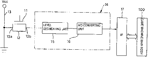
A microprocessor unit 14 (abbreviated to MPU, hereinafter) for controlling the
S control apparatus 200 is mounted on an internal board of the control
apparatus 200. The
MPU 14 functions as a level segmenting unit {LS) 15 for segmenting the output
level of
the analog signal which is outputted by the pressure-sensitive device 12 into
a plurality
of levels, and an A/D converting unit 16 for converting the , analog signal
which is
outputted from the pressure-sensitive device 12 into a digital signal in
accordance with
the output level which is segmented by the level segmenting unit 15. The
electrode 12b
of the pressure-sensitive device 12 is connected to an input side of the level
segmenting
unit 15.
The level segmenting unit 15 has a fundamental function for segmenting the
range of a preset analog signal level (voltage) by a uniform width, as shown
in Fig. 4.
The number of segments can be set arbitrarily, and the example shown in Fig. 4
illustrates that the range of the analog signal level (voltage) is uniformly
segmented into
eight levels. Individual output levels L1 to L8 which are thus uniformly
segmented are
transmitted to the AID converting unit 16. Incidentally, the range of the
analog signal
Level which is uniformly segmented by the level segmenting unit 15 can be
arbitrarily
changed.
The AID converting unit 16 converts the 'analog signal which is segmented into
levels by the level segmenting unit Z 5 into a digital signal in accordance
with the output
level of the analog signal and outputs the digital signal. That is, digital
signals having a
plurality of bits are outputted by the A/D converting unit 16 in accordance
with the
output level L l to L8.
Herein, a description will be given of a specific example of the level
segmenting
unit 15 and A/D converting unit 16. It is assumed that the control apparatus
200 is
CA 02351093 2001-05-11
WO 01/19-t77 PCTLIP00/061I7
-13-
driven by a power supply voltage of 3.S V, and the analog signal which is
outputted by
the pressure-sensitive device 12 changes from 0 to 2.4 V It is also assumed
that the
level segmenting unit 1 S uniformly segments the output level ranging from 0
to 2.4 V
into eight levels. Then, one level has a level width of 0.3 V
S Therefore, the level segmenting unit 1 S segments the output levels of 2.4
to 2.1 V,
2.l tol.8V,1.8to1.SV,1.Stol.2V,1.2to0.9V,0.9to0.6V,0.6to0.3V,and0.3to
0 V of the analog signal which is outputted by the pressure-sensitive device
12 into
level I (Ll), level 2 (L2), level 3 {L3), level 4 (L4), level S (LS), level 6
(L6), level 7
(L7), and level 8 (L8), respectively.
The AID converting unit 16 assigns proper digital signals having a plurality
of
bits to the output levels which are level-segmented as disclosed above and
outputs the
digital signals. For instance, the digital signals having a plurality of bits,
e.g., 8 bits or
16 bits, are assigned to the output levels, and digital signals of "lf', "3F',
..., "ff'
(hexadecimal notation) are assigned to level 1, level 2, ..., level 8,
respectively, and are
1 S outputted.
The digital signal which has a plurality of bits and is outputted by the A/D
converting unit 16 is transmitted to the game machine main body 100 via an
interface
17 which is provided in the internal board of the control apparatus 200, so
that the
digital signal causes the game character to be moved, etc.
The change in level of the analog signal outputted by the pressure-sensitive
device 12 corresponds to the change in pressure applied by the controller I1,
as
mentioned above. Accordingly, the digital signal which has a plurality of bits
and is
outputted by the A/D converting unit 16 corresponds to the pressure on the
controller 11
applied by the user. If the operations for the game character, etc. are
controlled in
2S response to the digital signal having a plurality of bits which is related
to the user's
pressing operation, it is possible to realize a smoother operation in an
analog manner, as
compared with the ON/OFF control operation in response to a single bit digital
signal
CA 02351093 2001-05-11
WO 01119-477 PCTlJPOO/OG117
-14-
which is "1" or "0".
According to the present embodiment, as shown in Fig. 5, the first to fourth
control units 210, 220, 230, and 240 have the configuration having controller
11 and
pressure-sensitive device 12 shown in Fig. 3. Thus, it is possible to
separately use
digital operation and analog operation of the control units 210, 220, 230, and
240.
Incidentally, only the control unit which is arbitrarily selected among the
first to fourth
control units 210, 220, 230, and 240 can also have the configuration shown in
Fig. 3.
As explained above, the level segmenting unit 15 uniformly segments the output
level of the analog signal which is outputted by the pressure-sensitive device
12 within
the preset range. However, if the preset range deviates from the range of the
analog
signal Level (voltage) which is actually outputted by the pressure-sensitive
device 12,
there is a danger that it is impossible to output a digital signal which
matches with state
of the controller 11.
Further, the pressure-sensitive devices 12 have individual difference and the
power supply voltages also vary. This results in varying output ranges of the
analog
signals which are outputted by the pressure-sensitive devices 12 that are
provided in the
control units 210, 220, 230, and 240, depending on the individual control
apparatuses
200.
According to the present embodiment, the control apparatus 200 comprises a
calibration function (segmenting-range adjusting unit) for individually
setting the range
of output levels of the analog signal which is segmented by the level
segmenting unit 15.
Fig. 6 is a block diagram showing a first structural example for calibration
of the
level segmenting unit 15. According to the configuration shown in Fig. 6, the
MPU 14
includes a memory 20 and the range of output levels of the analog signal which
is
segmented by the level segmenting unit 15 is stored in the memory 20.
As an example, in the production line of the control apparatus 200, a
predetermined load is applied to the control apparatus 200 so that the
resistance of the
CA 02351093 2001-05-11
WO 01/19477 PCT/JP00/06117
-15-
pressure-sensitive device 12 becomes a maximum. In this case, the output level
of the
analog signal which is outputted by the pressure-sensitive device 12 is stored
in the
memory 20.
Next, a description will be given based on the above-discussed specific
example.
Assuming that a default value of the level segmenting unit I S is set so as to
uniformly
segment the voltage level ranging 0 to 2.4 V into eight levels and an analog
signal of 2.0
V is outputted by the pressure-sensitive device 12 when the predetermined load
acts, the
A/D converting unit 16 outputs the digital signal "3f' which corresponds to
level 2, as
explained above. The digital signal "3f' is stored in the memory 20, and the
level
segmenting unit I S adjusts the output range of the analog signal which is
level-
segmented on the basis of the set value.
Incidentally, the digital signal "3f' corresponds to the output level of the
analog
signal of 2.1 V to I.8 V. Preferably the voltage value within the range is
specified in
advance. For instance, it is specified in advance that a maximum voltage value
(2.1 V
1 S in the foregoing example) of the output levels is the upper limit of the
range of output
levels of the analog signal which is segmented into the levels.
Fig. 7 is a block diagram showing a second structural example for calibration
of
the level segmenting unit. According to the configuration shown in Fig. 7, a
memory is
not provided in the control apparatus 200 and, in place thereof, the range of
output
levels of the analog signal which is segmented by the level segmenting unit 1
S is stored
in a built-in memory I11 of the game machine main body 100 to which the
control
apparatus 200 is connected or into a memory card 112 which is detachable.
When the calibration of the level segmenting unit 15 is executed by using the
configuration, preferably, a setting program for executing the calibration
operation is
built in a control program which is stored in a ROM 110 in the game machine
main
body 100.
Fig. 8 is a flowchart showing one example of the setting program.
CA 02351093 2001-05-11
WO O1/i9.177 PCT/.TP00/06117
- 16-
First of all, a power supply of the game machine main body 100 is turned on
(step S1). The sensitivity setting (calibration) of the control unit is
selected by the menu
selection by the user (step S2). Then, a setting screen is displayed on the
television
receiver 120 {step S3). For example, a message for prompting the user to
strongly press
the controller 11 which is provided in the predetermined control unit is
displayed on the
setting screen. When the user presses the controller 11 strongly according to
the
representation, the output level of the analog signal from the pressure-
sensitive device
12 which is detected in this case is outputted to the game machine main body
100 (step
S4). The output level is stored in the built-in memory 111 (step SS). The
above-
mentioned steps are repeated for each level segmenting unit 15 in the control
apparatus
200 {step S6), and the sensitivity setting of the control unit ends.
The level segmenting unit 15 provided in the control apparatus 200 adjusts the
range of output levels of the segmented analog-signal on the basis of the set
value which
is stored in the built-in memory 111 in the game machine main body 100.
It is also possible to provide the setting program for executing the
calibration
operation in the game program which is recorded in the optical disk.
Fig. 9 is a flowchart showing another example of the setting program.
To start with, the optical disk is loaded in the game machine main body 100
(step
S 10). Thereafter, it is checked to see if the memory card 112 is loaded in
the game
machine main body 100 (step S11). If the memory card 112 is not loaded, the
user's
menu-selection causes the selection of the sensitivity setting (calibration)
of the control
unit (step SI2), and the setting screen is displayed on the television
receiver 120 (step
S 13). For instance, a message for prompting to the user to strongly press the
controller
11 which is provided in the predetermined control unit is displayed on the
setting screen.
2S When the user strongly presses the controller 11 according to the
representation, the
output level of the analog signal from the pressure-sensitive device 12 which
is detected
in this case is outputted to the game machine main body 100 (step S 14). The
output
CA 02351093 2001-05-11
WO 01/19477 PCT/JP00/06117
-17-
level is stored in the built-in memory 111 (step S 15). The above-mentioned
steps are
repeated for each level segmenting unit 15 in the control apparatus 200 (step
S16), and
the sensitivity setting of the control unit ends.
If it is detected in step S11 that the memory card 112 is loaded, it is
checked to
determine if a set value regarding a calibration has already been stored in
the memory
card 112 (step S 17). If the result is YES in step S 17, the sensitivity
setting of the
control unit ends. In this case, the level segmenting unit 15 provided in the
control
apparatus 200 adjusts, on the basis of the set value which is stored in the
memory card
112, the range of output levels of the analog signal which is to be segmented.
If there is no set value regarding the calibration stored in the memory card
112,
the processing sequence proceeds to step S 12, and the above-mentioned
calibration
operation is performed. Then, the output level of the analog signal from the
pressure-
sensitive device 12 which is detected in step S 15 is stored in the memory
card 112 (step
S 16).
The level segmenting unit 15 provided in the control apparatus 200 adjusts, on
the basis of the set value which is stored in the built-in memory 111 in the
game
machine main body 100 or memory card 112 therein, the range of output levels
of the
analog signal which is to be segmented.
Fig. 10 is a block diagram showing a third structural example for calibration
of
the level segmenting unit 15. According to the configuration shown in FIG. 10,
two
volume devices 21 and 22 (serving as electric-potential setting devices) are
serially
connected to the power line 13 to which the pressure-sensitive device 12 of
the control
apparatus 200 is connected. The volume devices 21 and 22 enable an
intermediate
voltage of the power line 13 to be adjusted.
The level segmenting unit 15 sets the range of output levels of the segmented
analog-signal on the basis of intermediate voltages V 1 and VZ of the power
line 13
which are adjusted by the volume devices 21 and 22, as shown in Fig. 11. In
other
CA 02351093 2001-05-11
WO 01/19-t77 FCT/.1F00/06117
-18-
words, the level segmenting unit 15 sets the intermediate voltage Vl, which is
detected
by one volume device 21 on the side near the power source Vcc to the maximum
value
in the range of output levels of the segmented analog-signal, sets the
intermediate
voltage V2, which is detected by the other volume device 22, to the minimum
value in
the range of output levels of the segmented analog-signal, and uniformly
segments the
output level of the analog signal, which is outputted by the pressure-
sensitive device 12
within the range of the intermediate voltage V1 to V2. The volume devices 21
and 22
may be adjusted, for instance, upon shipment of the control apparatus 200.
If monitoring functions for the intermediate voltages V1 and V2 are added
to.the
level segmenting unit 15 and the secular change, etc. fluctuate the
intermediate voltages
V 1 and V2, the range of output levels of the segmented analog-signal may be
adjusted
on the basis of the intermediate voltages V 1 and V2 after the fluctuation. If
the thus-
constructed auto-calibration function is added, it is possible to always
maintain the
proper setting when the intermediate voltages V 1 and V2 fluctuate in
accordance with ~ - ~ - ~ --
the secular change of the pressure-serisitive device 12 and volume device and
variations
in the power supply voltage, because the range of output levels of the
segmented
analog-signal is adjusted on the basis of the intermediate voltages V1 and V2
after
fluctuation.
However, if the level segmenting unit 15 always executes the auto-calibration,
there is a danger that the output to the game machine main body 100 is
delayed. In this
case, only when the power supply of the control apparatus 200 is turned on,
the level
segmenting unit 1 S may adjust, by checking the intermediate voltages V 1 and
V2 of the
power line I 3, the range of output levels of the analog signal to be
segmented.
Fig. 12 is a block diagram showing a fourth structural example for calibration
of
the level segmenting unit. According to the constitution shown in FIG. 12, the
two
volume devices 21 and 22 are inserted in series in the power line 13 to which
the
pressure-sensitive device 12 in the control apparatus 200 is connected and,
further, the
CA 02351093 2001-05-11
W O 01119:177 PCTlJP00/06117
- 19-
MPU 14 includes a comparator 23 and a memory 24.
The limit value of the range of output levels of the analog signal which is
segmented by the level segmenting unit 15 is stored in the memory 24 in
advance. For
example, an allowable voltage of the MPU 14 is stored in the memory 24 as a
limit
value. The comparator 23 always monitors the intermediate voltages V 1 and V2
which
are detected by the volume devices 21 and 22, and has a function for comparing
the
limit value which is stored in the memory 24 with the intermediate voltages V
1 and V2
(especially, V 1 ) and forcedly sending the limit value to the level
segmenting unit 15
when the intermediate voltage is over the limit value. If the limit value is
sent from the
comparator 23, the range of output levels of the analog signal which is
segmented on
the basis of the limit value is adjusted.
According to the above-described constitution, if an analog signal of an
excessive output level, which is above the processing capacity of the MPU 14,
is
outputted by the ~ pressure-sensitive device 12, the normal operation of the
MPU 14 can
be compensated.
Next, a detailed description is given of a structural example of the control
unit
which is provided in the control apparatus 200 according to the first
embodiment of the
present invention.
Fig. 13 to Fig. 15 are diagrams showing a first structural example of the
second
control unit.
The second control unit 220 comprises the four control buttons 221
constructing
the controller 11, an elastic body 222, and a sheet member 223 on which the
pressure-
sensitive devices 12 are provided, as shown in Fig. 14. As shown in Fig. 13,
the control
buttons 221 are mounted, from the back side thereof, to mounting holes 201 a
which are
formed in the upper surface of the device main body 201. The control buttons
221
mounted in the mounting holes 201a are movable in the axial direction.
The elastic body 222 is made of insulative rubber, etc., has elastic portions
222a
CA 02351093 2001-05-11
WO 01119-t77 PCT/JP00/06117
-20-
which are projected upward, and supports the lower ends of the control buttons
221 at
the upper surfaces of the elastic portions 222a. If the control buttons 222
are depressed,
sloping portions of the elastic portions 222a are bent and the upper surfaces
of the
elastic portions 222a move together with the control buttons 221. If the
pressures to the
control button 221 are removed, the sloping portions of the elastic portions
222a which
are bent are elastically restored and the control buttons 221 are pushed up.
That is, the
elastic body 222 functions as biasing means for restoring the control buttons
221, which
are depressed by the pressing operation, to the original positions.
The sheet member 223 is made of a thin-sheet material such as a flexible and
insulative membrane. The pressure-sensitive devices 12 are provided at proper
portions
of the sheet member 223. As shown in Fig. i 5, the pressure-sensitive devices
12 are
arranged so as to face the control buttons 221 via the elastic body 222.
According to the present structural example, a projection 221a is formed at
the
bottom of the control buttons 221 serving as the controller 11, and a concave
portion
I5 222b for supporting the projection 221a is formed in the elastic portion
222a of the
elastic body 222. If the control button 221 is pressed, the projection 221 a
presses the
pressure-sensitive device 12 via the concave portion 222b of the elastic
portion 222a.
As mentioned above, the resistance of the pressure-sensitive device 12 changes
in accordance with the pressure which is applied from the control button 221.
The
projection 221a is provided at the bottom of the control button 221 and the
projection
221 a presses the pressure-sensitive devices 12 so that the pressure can be
transmitted to
the pressure-sensitive devices 12 with high sensitivity.
However, as a result of pressing the pressure-sensitive device 12 by the
projection 221 a, the pressure which acts on the pressure-sensitive device 12
and the
concave portion 222b of the elastic body 222 becomes excessively large and
there is a
danger in the durability of the pressure-sensitive device 12 and the elastic
body 222
decreasing.
CA 02351093 2001-05-11
WO Ol/19-t77 PCT/JP00/06117
-21 -
Next, according to a second structural example shown in Fig. 16 and Fig. 17,
the
bottom of the control button 221 serving as the controller 11 is flat and the
whole of the
flat bottom presses the pressure-sensitive device 12. The elastic portion 222a
of the
elastic body 222 has no concave portion formed therein, and it supports the
bottom of
the control button 221 by the flat surface thereof. If thus construction is
used, although
the sensitivity with which the pressure from the control buttons 221 is
transmitted to the
pressure-sensitive device 12 is decreased, the advantage of improved
durability of the
pressure-sensitive devices 12 and the elastic body 222 is obtained.
Fig. 1$ and Fig. 19 are diagrams showing a third structural example of the
second control unit.
According to the third structural example shown in the figures, the pressure-
sensitive devices 12 are directly provided at proper portions on an internal
board 204
which is built in the control apparatus 200. By providing the pressure-
sensitive devices
12 on the internal board 204, the sheet member can be omitted and the number
of parts
can be reduced. Incidentally, of course, the pressure-sensitive devices 12 are
provided
at portions to which the pressure from the control buttons 221 is transmitted.
Fig. 20 and Fig. 21 are diagrams showing a structural example of the first
control
unit.
As shown in Fig. 20, the first control unit 210 comprises the cross-shaped
control
body 211, a spacer 212 for positioning the control body 211, and an elastic
body 213 for
elastically supporting the control body 211 and; further, as shown in Fig. 21,
has a
configuration in which the pressure-sensitive devices 12 are arranged at
positions which
face the control keys 211 a (controller 11 ) of the control body 211 via the
elastic body
213.
The overall/general structure of the first control unit 210 is well known from
Japanese Unexamined Patent Application Publication No. 8-163672, etc., and
thus a
detailed description is omitted. However, the control body 211 is assembled so
as to
CA 02351093 2001-05-11
WO 01119x77 PCT/JP00/06117
-22-
enable the control keys 211a (the controller) to be pressed to the sides of
the pressure-
sensitive devices 12 (Fig. 21) while a convex portion 212a having hemispheric
shapes
which is formed at the center of the spacer 212 is set at the fulcrum.
If the control key 211a serving as the controller 11 is pressed, the pressure
acts
on the pressure-sensitive device 12 via the elastic body 213 and the
resistance of the
pressure-sensitive device 12 changes in accordance with the magnitude of the
pressure.
The structural example shown in Fig. 21 illustrates that the pressure-
sensitive devices
12 are directly provided at proper portions on the internal board 204 which is
built in
the control apparatus 200. However, similarly to the structural example of the
second
control unit 220 shown in Figs. 14 and 15, the pressure-sensitive devices 12
can be
provided on the sheet member 23.
Fig. 22 and Fig. 23 are diagrams showing a structural example of the third
control unit.
The third control unit 230 comprises the two control buttons 231, a spacer 232
for positioning the control buttons 231 in the control apparatus 200, a holder
233 for
supporting the control buttons 231, an elastic body 234, and an internal board
235, and
has the pressure-sensitive devices 12 at proper portions on the internal board
235.
The overall/general structure of the third control unit 230 is also well-known
from Japanese Unexamined Patent Application Publication No. 8-163672, etc.,
and thus
a detailed description is omitted. However, the control buttons 231 can be
pressed
while being guided by the spacer 232. The pressure when the control buttons
231 are
pressed acts on the pressure-sensitive devices 12 via the elastic body 234.
The
resistance of the pressure-sensitive devices 12 is changed in accordance with
the
magnitude of the applied pressure. The structural example shown in Figs. 22
and 23
illustrate that the pressure-sensitive devices 12 are directly provided at
proper portions
of the internal board 235 which is built in the control apparatus 200.
However, similarly
to the structural example of the second control unit 220 shown in Fig. 14 and
Fig. 15,
CA 02351093 2001-05-11
WO 01/19-l77 PCT/JP00106117
- 23 -
the pressure-sensitive device 12 can also be provided on the sheet member 223.
Incidentally, the fourth control unit 240 is also constructed similarly to the
third
control unit 230.
Although the above description shows the structural examples in the case in
which the present invention is applied to the first to fourth control units
210, 220, 230,
and 240, the present invention is not limited to be applied to all of the
control units.
The control unit to which the present invention is applied can be selected
arbitrarily and
the other control units can have conventional constructions.
The first embodiment is described by using the pressure-sensitive devices 12
having the characteristics shown in Figs: 4 and 11. In other words, according
to the
characteristics, the resistance of the pressure-sensitive device 12 increases
and the
output voltage decreases in accordance with the increase in the pressure of
the controller
11. However, according to the first embodiment, it is also possible to use a
pressure-
sensitive device 12 having characteristics which are opposite to the above-
mentioned
characteristics.- In other words, according to the opposite characteristics,
the.resistance
of the pressure-sensitive device 12 decreases and the output voltage increases
in
accordance with the increase in the pressure of the controller 11. By using
the pressure-
sensitive device 12 having this opposite characteristics, the input
characteristics of the
level segmenting unit 15 need to be inverted. However, the pressure-sensitive
device 12
has characteristics in that a large voltage is not applied unless the
controller 11 is
pressed.
[Second embodiment]
Next, a detailed description is given of the structure according to a second
embodiment of the present invention. Incidentally, the same reference numerals
denote
the same portion as those of the first embodiment which have been already
described,
and thus a detailed description thereof is omitted.
CA 02351093 2001-05-11
WO 01119x77 PCT/JP00106117
-24-
Although according to the control device 200 of the f rst embodiment, the
pressure-sensitive device i 2 is used as a detecting device, while, according
to the
second embodiment which will be described hereinbelow, a detecting device
comprises
a resistor 40 and a conductive member 50.
Fig. 24A to Fig. 24C are diagrams showing one structural example of a second
control according to the present embodiment. Although only a single control
button
221 and the related structure are shown in the figures, a plurality of control
buttons 221
can be provided in the second control unit 220, each having the same structure
as the
structure shown in the figures by selecting the control button 221
arbitrarily.
In other words, the second control unit 220 according to the present
embodiment
comprises the control button 221 serving as the controller 11, the elastic
body 222, the
conductive member 50, and the resistor 40. The conductive member SO is made
of, e.g.,
conductive rubber having elasticity, and is formed with a peak shape in which
the top of
the peak is at the center. The conductive member SO is adhered to the inside
of the
L 15 ceiling surface of the elastic portion 222a which is formed in the
elastic body 222.
The resistor 40 is provided, for instance, on the internal board 204 so as to
face
the conductive member S0, and the conductive member 50 makes contact to the
resistor
40 in accordance with the pressing operation of the control button 221. The
conductive
member 50 is deformed in accordance with the pressure on the control button
221 {that
is, contact pressure with the resistor 40), thereby changing the contact area
with the
resistor 40, as shown in Figs. 24B and 24C. In 'other words, when the pressure
on the
control button 221 is small, the portion near the top of the conductive member
50
having a peak shape makes contact with the resistor 40, as shown in Fig. 248.
Further,
when the pressure on the control button 221 becomes larger, the conductive
member 50
is gradually deformed from the top thereof and the contact area becomes
larger.
Fig. 25 is a diagram showing the circuit configuration of the resistor 40, the
conductive member 50, and devices peripheral thereto. A variable resistor 42
in Fig. 25
CA 02351093 2001-05-11
WO 01/1977 PCT/JP00/06117
- 25 -
corresponds to the combination of the conductive member 50 and the resistor 40
in Figs.
24A to 24C. A fixed resistor 41 (not shown in Figs. 24A to 24C) is~ connected
to the
resistor 40. A power supply voltage Vcc is applied to the variable resistor 42
and the
fixed resistor 41 which are serially connected, that is, across electrodes 40a
and 40b.
The variable resistor 42 corresponds to the combination of the conductive
member 50 and the resistor 40. The resistance of the variable resistor 42
changes in
accordance with the contact area between the conductive member 50 and the
resistor 40.
That is, if the conductive member SO makes contact with the resistor 40, the
conductive
member 50 functions as a bypass for the resistor 40 and a current flows.
Therefore, the
contact portion is effectively short-circuited, so that the resistance of the
resistor 40
drops. As the contact area of the conductive member 50 becomes larger, the
resistance
of the resistor 40 decreases more.
The power supply voltage Vcc applied across the electrodes 40a and 40b is
divided by the variable resistor 42 whose resistance changes in accordance
with the.
1 S pressure on the control button 221 and the fixed resistor 41. Thus, the
output voltage
which is obtained from an output terminal 40c between the variable resistor 42
and the
fixed resistor 41 becomes larger as the resistance of the variable resistance
42 become
smaller and, on the other hand, the output voltage becomes smaller as the
resistance of
the variable resistance 42 becomes larger.
Fig. 26 is a diagram showing the characteristics of the analog signal
(voltage)
which is outputted from the output terminal 40c of the resistor 40.
To start with, since a voltage is applied to the resistor 40 when the power is
turned on, a predetermined analog signal (voltage) Vmin is outputted from the
output
terminal 40c until the control button 221 is pressed (a position "a" shown in
the figure).
Subsequently, since the resistance of the resistor 40 is not changed until the
conductive
member 50 makes contact with the resistor 40 when the control button 221 is
pressed,
the output from the resistor 40 is held at Vmin and is not changed. Further,
the control
CA 02351093 2001-05-11
WO 01119:477 PCTlJP00106117
-26-
button 221 is pressed and the conductive member 50 makes contact with the
resistor 40
(a pressing position "b" in the figure) and, thereafter, the contact area of
the conductive
member 50 with the resistor 40 increases in accordance with the pressure on
the control
button 221. Thus, the internal resistance of the resistor 40 decreases and the
analog
signal (voltage) which is outputted from the output terminal 40c of the
resistor 40
increases. When the conductive member 50 is deformed to the greatest extent,
the
analog signal (voltage) outputted from the output terminal 40c of the resistor
40 is equal
to a maximum value Vmax (a pressed position "c" in the figure).
Fig. 27 is a block diagram showing the main portion of the control apparatus
according to the second embodiment of the present invention.
According to the present embodiment, the MPU 14 provided on the internal
board of the control apparatus 200 comprises the level segmenting unit 15, the
A/D
converting unit 16, and the switch 18. According to the present embodiment,
the analog
signal (voltage) which is outputted from the output terminal 40c of the
resistor 40 is
inputted to the level segmenting unit 15, then, the output level of the analog
signal is
segmented into a plurality of levels by the level segmenting unit 15, and,
further, the
AID converting unit 16 converts the analog signal which is outputted by the
resistor 40
into a digital signal in accordance with the segmented output level.
The functions of the level segmenting unit 15 and AID converting unit 16 are
the
same as those of the aforementioned first embodiment. The level segmenting
unit 15
has a fundamental function for segmenting the range of levels of the analog
signal
(voltage) which is outputted from the resistor 40 by a uniform width, as shown
in Fig.
36. The number of segments can be arbitrarily set and, in the example shown in
Fig. 36,
the range of levels of the analog signal (voltage) is uniformly segmented into
eight
levels. The individual output levels L1 to L8 which are segmented uniformly as
discussed above are transmitted to the A/D converting unit 16. Incidentally,
the range
of levels of the analog signal which is uniformly segmented by the level
segmenting
CA 02351093 2001-05-11
WO 01119-177 PCTIJP00106117
-27-
unit 15 can be changed arbitrarily.
The AID converting unit I6 converts the analog signal level-segmented by the
level segmenting unit 15 into the digital signal in accordance with the output
level of the
analog signal and outputs the digital signal. In other words, the A/D
converting unit I6
outputs the digital signal having a plurality of bits in accordance with the
output levels
Ll to L8.
The A/D converting unit 16 assigns the digital signal having a proper
plurality of
bits to the output level which is level-segmented, and outputs the digital
signal. As an
example, the digital signal having a plurality of bits, e.g., 8 bits or 16
bits is assigned to
the output level and the digital signals "lf', "3f', ..., "ff" are assigned
and outputted in
the cases of level 1 (L1), level 2 (L2), ..., the level 8 (L8), respectively.
The digital signal having .a plurality of bits which is outputted by the A/D
converting unit 16 is transmitted to the game machine main body 100 by way of
the
interface 17 that is provided to the internal board of the control apparatus
200. The
w 15 digital signal causes the movement of the game character, etc.
The level change in the analog signal which is outputted from the output
terminal
40c of the resistor 40 corresponds tv the change in the pressure which is
applied by the
control button 221 (controller 11 ). Therefore, .the digital signal having the
plurality of
bits which is outputted by the A/D converting unit 16 corresponds to the
pressure on the
control button 221 (controller 11 ) by the user. If the operation of the game
character, etc.
is controlled by the digital signal having the plurality of bits which has the
above-
explained relation with the user's pressing operation, it is possible to
realize a smoother
operation in an analog manner as compared with the control operation by the
digital
signal having a single bit ("1" or "0").
As described above, the level segmenting unit 15 uniformly segments the output
level of the analog signal which is outputted by the resistor 40 within a
predetermined
range. There is a danger that it is impossible to output a digital signal
which matches
CA 02351093 2001-05-11
CVO 01!19-177 PCT/JP00/06117
-28-
the state of the controller 11 if the predetermined range deviates from the
range of levels
of the analog signal (voltage) which is actually outputted by the resistor 40.
However, the resistor 40 and the conductive material 50 have individual
differences and the power supply voltage also varies. Consequently, the
individual
S control apparatuses 200 cause the output range of the analog signal
outputted by the
resistor 40 to differ.
Then, the control apparatus 200 according to the present embodiment comprises
a segmenting-range setting unit 25 for individually setting the range of
output levels of
the analog signal which is segmented by the level segmenting unit 15 (refer to
Fig. 27),
and to thereby calibrate the range of tevels of the analog signal (voltage)
which is
segmented by the level segmenting unit 1 S.
Fig. 28 is a diagram used to explain the function of the segmenting-range
setting
unit.
As shoivii in Fig. 28, a minimum value Vmin and a maximum value Vmax of the
analog signal {voltage) which is outputted by the resistor 40 are initially
set in advance
in the segmenting-range setting unit 25. An arbitrary allowable value a for
the
maximum value Vmax is set in advance. The allowable value a is set so as to
compensate for variations when the output (analog signal) of the resistance is
recognized on the basis of information from the AID converting unit 16.
Further, a
discriminating value y around the minimum value Vmin is set in advance so as
to
determine whether or not the control button is pressed.
For the setting, the segmenting-range setting unit 25 executes the calibration
operation as follows.
When the power source of the control apparatus 200 is turned on, the
2S segmenting-range setting unit 25 recognizes a level Vmin(Real) of the
analog signal
(voltage) which is actually outputted by the resistor 40 on the 'basis of the
information
from the AID converting unit 16 in order to adjust the minimum value Vmin of
the
CA 02351093 2001-05-11
WO 01/19-t77 PCT/JP00/06117
-29-
analog signal (voltage) which is outputted by the resistor 40.
In this case, considering the reason that the user presses the control button
221,
etc., it is determined whether or not Vmin(Real) is within the range of the
allowable
error value y in which Vmin is set to a center value. If Vmin(ReaI) is out of
the range
(Vmin+ y } > Vmin{Real) > (Vmin- y ), the user is informed that the
calibration is
being performed.
To inform the user, it is possible to adopt methods of switching on/off the
display
unit 253 which is provided in the control apparatus 200 and operating a
vibration
mechanism if such a mechanism is built in the control apparatus 200, etc.
Next, under the condition such that Vmin(Real) is within the range (Vmin+ y )
>
Vmin(Real) > (Vmin - y ), the value Vmin(Real) is compared with Vmin. As a
comparison, if Vrnin{Real) > Vmin, the initial set value Vmin is set as the
minimum
value of the analog signal (voltage) which is outputted by the resistor 40. If
Vmin(Real)
< Vmin, the actual output-value Vmin(Real) changes and set as the minimum
value of
the analog signal (voltage) which is outputted by the resistor 40.
Sequentially, the control button 221 is depressed strongly by the user
according
to the manual operation, etc, thereby recognizing a level Vmax(Real) of the
analog
signal (voltage) which is actually outputted by the resistor 40 on the basis
of the
information that is then outputted from the A/D converting unit 16.
If the value Vmax(Real) is larger than (Vmax - a ) which is obtained by
considering the allowable value a, it is recognized that the user pressed the
control
button 221 up to the limit and Vmax(Real) is compared with Vmax. As a
comparison,
Vmax(Real) < Vmax, the initial set value Vmax is set as the maximum value of
the
analog signal (voltage) which is outputted by the resistor 40. On the other
hand, if
Vmax(Real) > Vmax, the actual output value Vmax(Real} changes and set as the
maximum value of the analog signal (voltage) which is outputted by the
resistor 40.
The segmenting-range setting unit 25 controls the level segmenting unit 15 so
as
CA 02351093 2001-05-11
WO 01/i9~77 PCT/JP00/06117
-30-
to uniformly segment the analog signal (voltage) which is outputted by the
resistor 40
within the range from the minimum value Vmin to the maximum value Vmax, which
are set as mentioned above.
Fig. 29 is a diagram showing a structural example of the first control unit
S according to the present embodiment.
According to the structural example of the first control unit 210 shown in the
figure, corresponding to the control keys 211 a (controller 1 I ) of the cross-
shaped
control body 211, the conductive members SO are adhered to the inside ceiling-
surface
of the elastic body 213. The resistor 40 having a single construction is
disposed so as to
face the conductive members S0.
Fig. 30 is a diagram showing the circuit configuration of the resistor. As
shown
in the figure, the resistor 40 is inserted in series with the power line 13
and a voltage is
applied across the electrodes 40a and 40b. The internal resistance of the
resistor 40 is
schematically divided into first and second variable resistors 43 and 44 shown
in the
I S figure. For instance, the conductive member SO which moves together with
the control
key 211a (up directional key) for moving the character upward makes contact
with a
portion of first variable resistor 43 and the conductive member SO which moves
together
with the control key 2lla (left directional key) for moving to the left makes
contact
therewith, thereby changing the resistance in accordance with the contact area
with the
conductive members S0. For instance, the conductive member SO which moves
together with the control key 211 a (down directional key) for moving the
character
downward makes contact with the second variable resistor 44 and the conductive
member SO which moves together with the control key 211a (right directional
key) for
moving to the right makes contact therewith, thereby changing the resistance
in
2S accordance with the contact area with the conductive members S0.
The output terminal 40c is provided at an intermediate portion between the
variable resistors 43 and 44, and the analog signal is outputted from the
output terminal
CA 02351093 2001-05-11
WO 01/19-X77 PCT/JP00/06117
-31 -
40c in accordance with the pressure on the control keys 21 la (controller 11).
The outputs from the output terminal 40c can be calculated by using a dividing
ratio of the resistances of the first and second variable resistors 43 and 44
have. If the
resistance of the first variable resistor 43 is R1, the resistance of the
second resistor 44
is R2, and the power supply voltage is Vcc, an output voltage V generated at
the output
terminal 40c can be expressed by the following expression.
V = Vcc X R2/(R1+R2)
Therefore, when the resistance of the first variable resistor 43 decreases,
the
output voltage increases. On the other hand, when the resistance of the second
variable
resistor 44 decreases, the output voltage decreases.
Fig. 31 is a diagram showing the characteristics of the analog signal
(voltage)
which is outputted by the output terminal 40c of the resistor.
First of all, a voltage is applied to the resistor 40 when the power is turned
on, so
that a predetermined analog-signal (voltage) Vo is outputted bythe output
terminal 40c
unless the control keys 211 a of the controller 221 are pressed.
Next, if any one of control keys 211 a is pressed, the output from the
resistor 40 is
kept at Vo and does not change because the resistance of the resistor 40 does
not change
until the conductive member 50 makes contact with the resistor 40.
Moreover, the up directional key or the left directional key is pressed and
the
conductive member SO makes contact with the first variable resistor 43 in the
resistor 40
(a pressed position p in the figure) and, thereafter, the contact area of the
conductive
member 50 for the first variable resistor 43 increases corresponding to the
pressure on
the control key 211 a (controller). Thus, the resistance corresponding to the
position
decreases and the analog signal (volta.ge) which is outputted by the output
terminal 40c
in the resistor 40 is increased. When the conductive member 50 is deformed to
the
greatest extent, the analog signal (voltage) which is outputted by the output
terminal 40c
in the resistor 40 is set to the maximum value Vmax (a pressed position q in
the figure).
CA 02351093 2001-05-11
WO 01/19477 PCT/JP00/06117
-32-
On the contrary, the down directional key or right directional key is pressed
and
the conductive member 50 makes contact with the second variable resistor 44 in
the
resistor 40 (a pressed position r in the figure) and, thereafter, the contact
area of the
conductive member 50 for the second variable resistor 44 increases
corresponding to the
pressure on the control key 211a (controller). Thus, the resistance
corresponding to the
position decreases and this results in decreasing the analog signal (voltage)
which is
outputted by the output terminal 40c in the resistor 40. When the conductive
member
50 is deformed to the greatest extent, the analog signal (voltage) which is
outputted by
the output terminal 40c in the resistor 40 is set to the minimum value Vmin (a
pressed
position s in the figure).
The analog signal (voltage) which is outputted by the output terminal 40c in
the
resistor 40 is inputted to the level segmenting unit 15, as shown in Fig. 32.
The level
segmenting unit 15 segments the output level of the analog signal into a
plurality of
levels and, further, the AID converting unit 16 converts the analog signal
which is
I S outputted by the resistor 40 into the digital signal in accordance. with
the segmented
output-level. Incidentally, the functions of the level segmenting unit 15 and
the AlD
converting unit 16 which are shown in Fig. 32 have been described above with
reference to Fig. 27, and the detailed description thereof is omitted.
The value Vo during the non-pressed state and the minimum value Vmin and the
maximum Vmax of the analog signal (voltage) which is outputted by the resistor
40 are
initially set, in advance, in the segmenting-range setting unit 25 for
individually setting
the range of output levels of the analog signal which is segmented by the
level
segmenting unit I5, as shown in Fig. 33. An arbitrary allowable value a for
the
maximum value Vmax is preset and an arbitrary allowable value ~ for the
minimum
value Vmin is preset. The allowable values a and J3 compensate for variations
when
the output (analog signal) of the resistance is recognized on the basis of the
information
from the A/D converting unit 16. Further, a discriminating value y around the
value
CA 02351093 2001-05-11
WO 01/19:177 PCT/JP00/06117
-33-
Vo of the analog signal (voltage) which is outputted in the non-pressed state
is preset so
as to determine whether or not the control button is pressed.
For the setting, the segmenting-range setting unit 25 executes the calibration
operation as follows.
When the power supply of the control apparatus 200 is turned on, the
segmenting-range setting unit 25 first recognizes, on the basis of information
from the
A/D converting unit 16 in order to adjust the level Vo of the analog signal
(voltage)
which is outputted by the resistor 40 in the non-pressed state, a level
Vo(Real) of the
analog signal (voltage) which is actually outputted by the resistor 40.
In this case, considering the reason that the user presses the control button
221,
etc., it is determined whether or not Vo(Real) is within the range of the
allowable error
value y in which Vo is set as a central value. If Vo(Real) is out of a range
(Vo+ y ) >
Vo(Real) > (Vo- y ), the user is informed that the calibration is being
performed.
To inform the user, it is possible to adopt methods of switching on/off the
display
unit 253 provided in the control apparatus 200 and operating a vibration
mechanism if
such a mechanism is built in the control apparatus 200, etc.
Next, under the condition such that Vo(Real) is within the range (Vo+ y ) >
Vfl(Real) > (Vo- y ), the value Vo(Real) is compared with Vo. As a comparison,
if
Vo(Real) > Vo, the initial set value Vp is set as the value of the analog
signal (voltage)
which is outputted by the resistor 40 in the non-pressed state. On the other
hand, if
Vp(Real) < Vo, the actual output value Vo(Real) changes and set as the value
of the
analog signal (voltage) which is outputted by the resistor 40 in the non-
pressed
operation.
Sequentially, the up directional key is depressed strongly by a manual
operation
of the user, etc, thereby recognizing the level Vmax(Real) of the analog
signal (voltage)
which is actually outputted by the resistor 40 on the basis of information
that is then
outputted from the AID converting unit 16.
CA 02351093 2001-05-11
WO Oii19a77 PCT/JP00/Obli7
-34-
If .the value Vmax(Real) is larger than (Vmax - a) which is obtained by
considering the allowable value a, it is recognized that the user pressed the
up
directional key up to the limit and Vmax(Real) is compared with Vrnax. As a
comparison, Vmax(Real) < Vmax, the initial set value Vmax is set as the
maximum
value of the analog signal (voltage) which is outputted by the resistor 40. On
the other
hand, if Vmax(Real) > Vmax, the actual output value Vmax{Real) changes and set
as
the maximum value of the analog signal (voltage) which is outputted by the
resistor 40.
The similar operation is performed in the case of the left directional key.
The
maximum value Vmax of the analog signal (voltage) which is outputted by the
resistor
40 in accordance with the operation for pressing the left directional key is
set.
Sequentially, the down directional key is depressed strongly by a manual
operation of the user, etc, thereby recognizing the level Vmin{Real) of the
analog signal
(voltage) which is actually outputted by the resistor 40 on the basis of
information that
is then outputted by the A/D converting unit 16.
If the value Vmin(Real) is smaller than (Vmin+ a ) which is obtained by
considering the allowabte value (3 , it is recognized that the user pressed
the down
directional key up to the limit and Vmin(Real) is compared with Vmin. As a
comparison, if Vmin(Real) > Vmin, the initial set value Vmin is set as the
minimum
value of the analog signal (voltage) which is outputted by the resistor 40. On
the other
hand, if Vmin(Real) < Vmin, the actual output value Vmin(Real) changes and set
as the
minimum value of the analog signal (voltage) which is outputted by the
resistor 40.
The similar operation is performed in the case of the right directional key.
The
minimum value Vmin of the analog signal (voltage) which is outputted by the
resistor
40 in accordance with the operation for pressing the right directional key is
set.
The segmenting-range setting unit 25 controls the level segmenting unit 15 so
as
to uniformly segment the analog signal (voltage) which is outputted by the
resistor 40
within the range from the output Vo in the non-pressed state to the maximum
value
CA 02351093 2001-05-11
WO 01/19.177 PCT/JP00/06117
-35-
Vmax, which are set as mentioned above, in response to the pressing operation
of the up
directional key and the left directional key. The segmenting-range setting
unit 25
controls the level segmenting unit 15 so as to uniformly segment the analog
signal
(voltage) which is outputted by the resistor 40 within the range from the
output Vo in
the non-pressed state to the minimum value Vmin, which are set as mentioned
above, in
response to the pressing operation of the down directional key and the right
directional
key.
Incidentally, in the above description, the up directional key and the left
directional key are assigned to the first variable resistor portion in the
resistor 40 and the
down directional key and the right directional key are assigned to the second
variable
resistor portion in the resistor 40. However, the present invention is not
limited to the
above description and, obviously, it is possible to arbitrarily set the
allocation between
the keys and the variable resistor portions.
With respect to the first control unit 210, the resistor 40 can also be
individually
arranged at the conductive members 50 which are provided at positions
corresponding
to the control keys 221a of the control body 211, so as to have the circuit
configuration
shown in Fig. 25. In this case, the characteristics of the analog signal
(voltage) which is
outputted by the output terminal 40c in the resistor 40 are those shown in
Fig. 26.
jModified examples of detecting device]
Next, a description is given of modified examples of the detecting device
comprising the resistor 40 and the conductive member 50. Although according to
the
following description relates to the detecting device which is provided in the
second
control unit 220 as an example, it is possible to apply another control unit
to the
following detecting device.
Figs. 34A to 34D to Figs. 37A to 37D show detecting devices which are obtained
by changing the shape of the conductive member 50. Incidentally, in the
figures, Figs.
CA 02351093 2001-05-11
WO 01/19-i77 PCT/JP00/06117
-36-
34A, 35A, 36A, and 37A are front sectional views of the control unit including
the
detecting device, Figs. 34B, 35B, 36B, and 37B are front views of the
conductive
member, Figs. 34C, 35C, 36C, and 37C are diagrams in which the conductive
member
is seen from below, and Figs. 34D, 35D, 36D, and 37D are characteristic
diagrams of
the analog signal which is outputted by the output terminal of the resistor.
Any conductive member 50 in the figures have a shape in which the contact area
with the resistor 40 can be changed in accordance with the contact pressure
with the
resistor 40.
That is, according to the detecting device shown in Figs. 34A to 34D, the
conductive members 50 is formed with a shape having a trapezoidal longitudinal-
section surface (like a truncated cone in the figures). According to the
conductive
member 50 having such a shape, a top portion 50a of the conductive member 50
makes
contact with the resistor 40 in accordance with the pressing operation of the
control
buttons 221. However, the top portion 50a has a flat surface, so that the
resistance
decreases largely at the contact instant and this results in rapid increase in
the output
voltage (analog signal) as shown in Fig. 34D and, thereafter, the output
voltage
successively changes in accordance with the pressure.
Accordingly, the instant the conductive member 50 is connected and
disconnected to the resistor 40, a digital ON/OFF operation can be realized.
Although
Figs. 34A to 34D illustrate the conductive member 50 having a shape like a
truncated
cone, the conductive member 50 can also be foimed so as to have a truncated
multi-
pyramid in which the number of angles is three or four or more as an example.
The detecting device 50 shown in Figs. 35A to 35D uses the conductive member
50 having a shape in ribs 50b in the vertical direction are formed to the
peaked
peripheral-surfaces. It is dangerous for the peaked conductive-member 50 shown
in
Figs. 24A to 24C that a buckling occurs when the acting direction of the
pressure is
inclined from the central axis. Then, as shown in Figs. 35A to Fig. 35D, the
ribs 50b
CA 02351093 2001-05-11
WO 01/19=t77 PCT/JPOO/OG117
-37-
are formed to the peripheral surface of the conductive member 50 and,
consequently, the
buckling of the conductive member 50 can be suppressed. The shape exhibits a
remarkable acting-effect by combining, especially, the cross-shaped
controlling body
21 I shown in Fig. 29 with the conductive member 50.
The detecting device shown in Figs. 36A to 36D is formed with a shape having a
spherical surface of the conductive member S0. As mentioned above, by forming
the
spherical conductive-member S0, the buckling of the conductive member 50 can
be
avoided.
According to the detecting device shown in Figs. 37A to 37D, the conductive
I0 member SO is formed with a peaked shape having steps. The cross-sectional
area
decreases step by step towards the top of the conductive member 50 facing the
resistor
40. According to the conductive member SO having such a shape, the amount of
deformations increases in accordance with the increase in pressure. However,
in the
step thereof, when a step portion 50c makes contact with the resistor 40, the
contact area
rapidly becomes large and the resistance decreases. The analog signal which is
outputted by the output terminal of the resistor 40 changes step by step, as
shown in Fig.
37D. Therefore, the conductive member 50 has characteristics in that the
boundary at
which the analog output changes rapidly can be readily recognized and stable
level-
segment is easy. Since the analog output changes step by step in response to
the
pressure, the user can easily adjust the pressure.
Figs. 38A to 38D to Figs. 40A to 4OD show detecting devices which are obtained
by changing a shape of the conductive member 50. Incidentally, in the figures,
Figs.
38A, 39A, and 40A are front sectional views of the control unit including the
detecting
device, Figs. 38B, 39B, and 40B are front views of the conductive member,
Figs. 38C,
39C, and 40C are diagrams in which the conductive member is seen from below,
and
Figs. 38D, 39D, and 40D are characteristic diagrams of the analog signal which
is
outputted by the output terminal of the resistor.
CA 02351093 2001-05-11
WO 01/19-t77 PCT/JP00/06117
-38-
Any resistor 40 shown in the figures have a shape in which the cross-sectional
area decreases towards the top facing the conductive member S0. According to
the
detecting device shown in Figs. 38A to 38D, the resistor 40 is formed with a
peaked
shape. When the conductive member 50 descends together with the control
buttons 221,
the conductive member 50 makes contact with the resistor 40 and is deformed.
Since
the resistor 40 has the peaked shape, the contact area with the conductive
member 50
sequentially becomes larger in accordance with the pressure. Then, the analog
signal
which is outputted by the output terminal of the resistor 40 sequentially
changes, as
shown in Fig. 38D.
According to the detecting device shown in Figs. 39A to 39D, the resistor 40
is
formed with a shape having a trapezoidal longitudinal-section surface (like a
truncated
cone in the figures). The conductive member SO first makes contact with a top
portion
40a of the resistor 40 having such a shape in accordance with the pressing
operation of
the control buttons 221. The top portion 40a has a flat surface, so that the
output
1 S voltage rapidly increases at the contact instant, as shown by "a" in Fig.
39D and,
thereafter, the output voltage sequentially changes in accordance with the
pressure.
Accordingly, the instant the conductive member 50 makes contact with the
resistor 40, the digital ON/OFF operation can be realized. Although Figs. 39A
to 39D
illustrate the resistor 40 having a shape like a truncated cone, the resistor
40 can also be
formed so as to have a truncated mufti-pyramid in which the number of angle is
three or
four or more as an example.
According to the detecting device shown in Figs. 40A to 40D, the resistor 40
is
formed with a spherical surface. The resistor 40 is formed as mentioned above,
so that
the detecting device shown in Figs. 40A to 40D can have almost the same
characteristics as those shown in Fig. 36A to 3bD.
According to a detecting device shown in Figs. 41 A to 41 D, the resistor 40
is
formed with a peaked shape having steps and the cross-section area decreases
step by
CA 02351093 2001-05-11
WO 01/19-X77 . PCT/JP00/06117
-39-
step towards the top of the resistor 40 facing the conductive member 50. In
the step in
which the conductive member 50 makes contact with the resistor 40 having such
a
shape while being deformed in accordance with the pressing operation, the
contact area
rapidly becomes large and the resistance decreases when the conductive member
50
makes contact with a step portion 40b of the resistor 40. The analog signal
which is
outputted by the output terminal of the resistor 40 changes step by step, as
shown in Fig.
41D. Therefore, the conductive member SO has characteristics in that the
boundary at
which the analog output rapidly changes can be readily recognized and stable
level-
segment is easy. Since the analog output changes step by step in response to
the
pressure, the user can easily adjust the pressure.
According to a detecting device shown in Figs. 42A to 42D, the conductive
member 50 is formed with a peaked shape, a contact legion in the resistor 40
with the
conductive member 50 is segmented by spaces 41, and the contact area increases
step
by step in accordance with the deformation of the conductive member 50.
Specifically
speaking, the resistor 40 is formed with a shape shown in Figs. 42B to 42D
According to the detecting device having a structure shown in the figures, the
top
of the conductive member 50 first makes contact with a center portion 40c of
the
resistor 40 in accordance with the pressing operation of the control buttons
221.
Thereafter, the conductive member 50 is deformed in accordance with the
increase in
pressure and, then; a contact region of the conductive member 50 becomes
larger step
by step in order of outer-peripheral portions 40d, 40e, and 40f of the
resistor 40. In
association therewith, the resistance decreases.
Intervals among portions 40a to 40f of the resistor 40 are segmented by the
spaces 41, so that the resistance does not change and the output voltage
(analog signal)
thus is almost constant while the conductive member SO passes through the
spaces 41.
Therefore, the analog signal which is outputted by the output terminal of the
resistor 40 changes step by step, as shown in Fig. 42D. The conductive member
50 has
CA 02351093 2001-05-11
WO 01/19:177 PCT/JP00/06117
-40-
characteristics in that the boundary at which the analog output rapidly
changes can be
readily recognized and stable level-segment is easy.
Incidentally, according to the detecting devices having the above-described
various structures, the arrangement of the resistor 40 and the conductive
member 50 in
the control unit can be inverted. As an example, Fig. 43 illustrates that if
the resistor 40
is adhered to the inside ceiling-surface of the elastic portion 222a which is
formed on
the elastic body 222 and the conductive member 50. is disposed at a position
facing the
resistor 40, the same function and advantage as the aforementioned detecting
devices
can be obtained.
The present invention is not limited to the above-described embodiments.
For instance, the control apparatus according to the present invention is not
limited to be applied to the control apparatus 200 for the video game machine
shown in
Fig. 2 and the digital operation and the analog operation are possible and,
thus, the
present invention can be applied to a variety of control apparatus whereby the
functions
can be improved.
According to the present invention, as explained above, the digital signal
having
a plurality of bits whereby the analog control operation is possible is
outputted by the
output unit for the digital signal having a plurality of bits in accordance
with the
pressing operation of the controller. Therefore, the digital operation can be
realized by
the controller for pressing operation.