Note : Les descriptions sont présentées dans la langue officielle dans laquelle elles ont été soumises.
CA 02354361 2001-07-31
Doc. No. 10-353 CA Patent
VIRTUAL WAVEPLATE AND OPTICAL CHANNEL INTERLEAVER FORMED
THEREWITH
Field Of The Invention
The present invention relates a device for imposing a retardance between
orthogonally
polarized components of an optical signal without the use of birefringent
material, and in
particular to a virtual waveplate that can be used in an optical channel
interleaver.
Background Of The Invention
Optical multiplexers are used in the wavelength division multiplexing (WDM) of
a
plurality of optical channels for transmission via a single carrier fiber. At
the receiving end of
the fiber, the same general techniques are used to demultiplex the optical
channels back into
individual channels once again. Adding more channels to an optical signal
increases the amount
of data that can be sent down an optical network without the laying down of
any additional fiber.
The demand for additional capacity on current fiber networks keeps increasing,
along with the
demand for lower cost equipment to minimize initial capital costs, and less
complicated
equipment to reduce installation and maintenance costs.
One solution to the aforementioned problem includes the use of interleaver
technology,
and in particular to the birefringent waveplate-based interleaver technology
disclosed in United
States Patents No. 4,566,761 issued January 28, 1986; and 4,685,773 issued
August 11, 1987
both to Carlsen et al. Birefringent materials are relatively costly and
temperature sensitive,
moreover, there is a limit to the size that a single crystal can be grown,
which could eventually
restrict the capacity of the system. Other interleaver technologies are based
on the Michelson
interferometer, and include a Gires Tournois etalon in one arm (EP 933,657,
filed January 8,
CA 02354361 2001-07-31
Doc. No. 10-353 CA Patent
1999 in the name of Dingel et al) or in both arms (US 6,169,626 issued January
2, 2001 in the
name of Chen et al). Michelson Gires Tournois (MGT) interleavers are
complicated to
manufacture due to the high degree of accuracy required to match both of the
arms thereof and to
tune one or more cavities, which are temperature sensitive.
An object of the present invention is to overcome the shortcomings of the
prior art by
providing a less costly virtual waveplate that uses passive elements, which
can be used in an
interleaver device. Another object of the present invention is to increase the
temperature
stability of the waveplate assembly and to enable reflection losses to be
minimized.
Summary of the Invention
Accordingly, the present invention relates to a device for introducing a
relative delay
between orthogonally polarized components of an input signal comprising:
an input port for launching the input signal;
beam splitting means for dividing the input signal into first and second
orthogonally polarized
sub-beams, and for directing the first sub-beam along a first path and the
second sub-beam along
a second path;
first reflecting means in the first path for redirecting the first sub-beam
back towards the beam
splitting means;
delay means in the first path for imposing a relative delay between the first
and second sub-
beams;
second reflecting means in the second path for redirecting the second sub-beam
back towards the
beam splitting means for recombination with the first sub-beam; and
an output port for outputting the recombined first and second sub-beams.
Another aspect of the present invention relates to an optical filter
comprising:
an first port for launching an input optical signal, which comprises a first
and a second set of
channels;
a second port for outputting the first set of channels;
a third port for outputting the second set of channels;
a first virtual waveplate; and
2
CA 02354361 2001-07-31
Doc. No. 10-353 CA Patent
polarized beam separating means for directing the first set of channels to the
second port, and for
directing the second set of channels to the third port. The virtual waveplate
comprises:
first beam splitting means for dividing the input signal into first and second
orthogonally
polarized sub-beams, and for directing the first sub-beam along a first path
and the
second sub-beam along a second path;
first reflecting means in the first path for redirecting the first sub-beam
back towards the
first beam splitting means;
second reflecting means in the second path for redirecting the second sub-beam
back
towards the first beam splitting means for recombination with the first sub-
beam forming
a first recombined signal; and
first delay means in the first path for imposing a first relative delay
between the first and
second sub-beams, whereby when the first and second sub-beams recombine, the
first set
of channels is orthogonally polarized relative to the second set of channels.
Brief Description of Drawings
This present invention will be more fully described with reference to the
accompanying
drawings, which illustrate preferred embodiments of the invention, wherein:
Figure 1 is a schematic representation of a conventional birefringent
waveplate-based
interleaver;
Figure 2 is a schematic representation of a virtual waveplate according to the
present invention;
Figure 3 is a schematic representation of the dual-pass interleaver including
the virtual waveplate
of Fig. 2 illustrating the beam paths;
Figure 4 is a schematic representation of another embodiment of an
interleaver, which includes
the virtual waveplate according to Fig. 2; and
Figure 5 is a schematic representation of a dual-input interleaver, which
includes the virtual
waveplate according to Fig. 2;
3
CA 02354361 2001-07-31
Doc. No. 10-353 CA Patent
Detailed Description
With reference to Figure 1, a conventional birefringent waveplate interleaver
includes a
first birefringent element 1 of length L and oriented with the optical axis at
45° with respect to
the polarization of the input beam (vertical), and a second birefringent
element 2 of length 2L
and oriented with the optical axis at 105° with respect to the
polarization of the input beam
(vertical). The use of birefringent elements of length L and 2L is the optical
version of adding
the first harmonic frequency to the fundamental frequency to build a filter
with a more square-
shaped channel response. Of course, if an infinite number of the harmonics
were added the
result would be an ideal square shape. When in use as a de-interleaver, a beam
of light 3 with
mixed polarization and a series of channels is launched through collimating
lens 4 into a
polarization beam sputter 6, e.g. a rutile crystal. The polarization beam
splitter 6 divides the
beam of light 3 into two orthogonally polarized sub-beams 7, only one of which
can be seen in
Figure 1. A half wave plate 8 is positioned in the path of one of the sub-
beams, so that both sub-
beams 7 will enter the first birefringent element 1 with the same polarization
(e.g. vertical as
shown in Fig. 1 ). After passing through the first and second birefringent
elements 1 and 2, the
state of polarization of the even channels in the sub-beams 7 effectively
remains the same, while
the state of polarization of the odd channels is rotated by 90°.
Accordingly, when the sub-beams
7 pass through a middle section 9 of a stacked polarization beam sputter 11,
the odd channels
sub-beams 12 (only one shown) are reflected towards the bottom section 13,
while the even
channel sub-beams 14 (only one shown) are passed through middle section 9 to
quarter wave
plate mirror 16. The quarter wave plate mirror 16 rotates the polarization of
the even channels
14 (e.g. vertical to horizontal) and reflects them back towards the middle
section 9, whereby they
4
CA 02354361 2001-07-31
Doc. No. 10-353 CA. Patent
are reflected to the top section 17 of the stacked polarization beam splitter
11. The even
channels are reflected in the top section 17, and pass through the second and
first birefringent
elements 2 and 1 for a second time. Again, the even channels 14 exit the
birefringent elements 1
and 2 with the same polarization as when they entered. A half wave plate 18
and a beam
combiner 19, e.g. a ruble crystal, are used to combine the two even channel
sub-beams 14 for
output via focusing lens 21. Similarly, the odd channel sub-beams 12 get
reflected in the bottom
section 13 towards the quarter wave plate mirror 16, which rotates the
polarization of the odd
channel sub-beams 12 (e.g. from horizontal to vertical), whereby they pass
through the bottom
section 13 and back through the second and first birefringent elements 2 and 1
for a second time.
Again, the odd channels 12 exit the birefringent elements 1 and 2 with
polarizations orthogonal
to when they entered, e.g. vertical to horizontal. A half wave plate 22 and a
beam combiner 23,
e.g. a ruble crystal, are used to combine the odd channel sub-beams 12 for
output via lens 24.
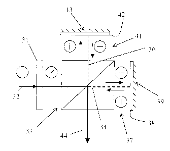
With reference to Figure 2, the virtual waveplate according to the present
invention
includes a half waveplate 31 oriented at an angle of 22.5° relative to
an input beam 32 of
polarized light providing a rotation of 45° thereto. The input beam 32
can be either horizontally
or vertically polarized; however in the illustrated example the input beam 32
is vertically
polarized. Moreover, the waveplate 31 can be eliminated if the light is input
in the appropriate
state of polarization. A polarization beam sputter (PBS) 33 splits the input
beam 32 into an s-
polarized (horizontal) sub-beam 34, which passes straight through the PBS 33,
and a p-polarized
(vertical) sub-beam 36, which is reflected in the PBS 33. The PBS is
preferably comprised of
two triangular prisms with a polarization sensitive coating therebetween. The
s-polarized
(horizontal) sub-beam 34 traverses a gap 37 of length d1 until being
intercepted by a quarter
wave plate 38 with a reflective rear surface 39. Two passes through the
quarter wave plate 38
CA 02354361 2001-07-31
Doc. No. 10-353 CA Patent
results in a 90° rotation of the polarization of the sub-beam 34, e.g.
from horizontal to vertical,
whereby when the sub-beam 34 re-enters the PBS 33 it gets reflected.
Similarly, p-polarized
sub-beam 36 traverses a gap 41 of length d2 until being intercepted by a
quarter wave plate 42
with a rear reflective surface 43. Accordingly, the p-polarized sub-beam 36 is
reflected back
towards the PBS 33 after a cumulative rotation of 90°, so that the PBS
33 will pass the sub-beam
36 therethrough for interference with the reflected sub-beam 34 forming
combined beam 44.
Therefore, the s-polarized (vertical) sub-beam and the p-polarized
(horizontal) sub-beam have
retardance between them defined by the difference between dl and d2, thereby
providing the
virtual equivalent of a waveplate. In practice dl or d2 can be equal to zero,
whereby the
difference would be dl or d2.
Since this device provides different paths for the o and a waves, surfaces in
the path of
the o waves can be coated with a different antireflective coating than the
surfaces in the path of
the a waves. Therefore, the effectiveness of the anti-reflective coatings can
be maximized in
each path, rather than having to compromise the effectiveness of the coating
when both types of
waves travel both paths. Moreover, this system is athermal, since the path
difference is provided
in air, not in some other material substance more susceptible to thermal
expansion.
With reference to Figure 3, two of the aforementioned virtual wave plates 48
and 49 of
Fig. 2 are arranged in an interleaver device as substitutes for the
birefringent elements 1 and 2
from Fig. 1. This configuration yields a flattop interleaver because the path
lengths dl and d2 of
this system are set to give the fundamental and first harmonic from lengths L
and 2L, which are
selected to provide the desired channel spacing. It is well known that the
summation of a
fundamental and the odd harmonics of the fundamental, yields a square wave
response, and that
6
CA 02354361 2001-07-31
Doc. No. 10-353 CA Patent
a summation of the fundamental and first harmonic gives a good approximation
of a square wave
response, i.e. a flattop filter.
When the illustrated interleaver device is used for de-interleaving optical
channels, a
beam of light 50 of mixed polarization comprising a plurality of channels is
launched through
input port 51. Port 51 comprises a lens 52, preferably a graded index (GRIN)
lens, a beam
sputter 53, preferably a ruble crystal, and a polarization rotator 54,
preferably a half wave plate.
Please note: in drawings 3,4 and 5 polarization rotators 54 are shown in side
view for clarity,
while the remainder of the figure is in plan view. The beam sputter 53
separates the input beam
50 into two orthogonally polarized sub-beams 56 (only one of which can be seen
in the Figure),
and the polarization rotator 54 rotates the polarization of one of the sub-
beams 56 so that both of
the sub-beams 56 have the same polarization. As described above, the input sub-
beams 56 are
passed through a half wave plate 57 oriented at an angle of 22.5°
thereto, resulting in the state of
polarization of the sub-beams 56 being rotated by 45°. A PBS 58 splits
the sub-beams 56 into
horizontally polarized sub-beams 59, which get passed therethrough, and
vertically polarized
sub-beams 60, which get reflected thereby. The horizontally polarized sub-
beams 59 are
directed through a quarter wave plate 62, and get reflected back by a
reflective surface 63. The
double pass through the quarter wave plate 62 results in the horizontally
polarized sub-beams
becoming vertically polarized, whereby they get reflected by the PBS 58 rather
than passed
therethrough. The quarter wave plate 62 is fixed to the side of the PBS 58
making the length
dl=0. The vertically polarized sub-beams 60 pass through a quarter wave plate
64 after
traversing a gap 66 of length d2=L defined by spacers 67. A shear plate 68 is
positioned in the
gap 66 to enable minor adjustments to the optical path length. The sub-beams
60 get directed
back through the PBS 58 by a reflective coating 69 on the quarter wave plate
64 after the state of
7
CA 02354361 2001-07-31
Doc. No. 10-353 CA Patent
polarization has been rotated by 90°. Accordingly, the two sets of sub-
beams 59 and 60
recombine into sub-beams 71 and are directed to the second virtual wave plate
49.
The recombined sub-beams 71 pass through a half wave plate 73, which is
oriented at an
angle of 52.5°, before entering a PBS 74. The PBS 74 again splits the
sub-beams 71 into
orthogonally polarized sets of sub-beams 76 and 77. Sub-beams 76 pass through
quarter wave
plate 78 and are directed back by reflective surface 79 after a 90°
rotation. Sub-beams 77
traverse a gap 80 of length 2L, defined by spacers 81, and pass through
quarter wave plate 82. A
reflective surface 83 on the quarter wave plate 82 directs the sub-beams 77
back through the PBS
74 for recombination with sub-beams 76. A sheer plate 84 positioned in the gap
80 enables
minor adjustments to be made to the optical path length of the sub-beams 77. A
half wave plate
96, oriented at an angle of 3.5°, is positioned between the PBS 87 and
the second virtual
waveplate 49 for making a minor adjustment to the state of polarization of the
sub-beams passing
therethrough.
Due to the appropriate phase delays caused by the gaps 66 and 80, and the
orientations of
the waveplates 57, 73 and 96, the channels in the recombined sub-beams 85 have
states of
polarization that alternate between vertical and horizontal. Accordingly, by
passing the
recombined beam 85 through the middle section 86 of a stacked PBS 87, the even
number
channels 88 can be separated from the odd number channels 89.
The odd channels 89, which have become horizontally polarized, pass through
the middle
section 86 of the PBS 87. A quarter wave plate 91, with a reflective coating
92, is positioned in
the path of the odd channels 89 for redirecting them back through the middle
section 86 of the
PBS 87 after a 90° rotation of their state of polarization. The odd
channels 89, which are now
vertically polarized, are reflected by the middle section 86 towards a lower
section 93 of PBS 87,
CA 02354361 2001-07-31
Doc. No, 10-353 CA Patent
which in turn reflects the odd channels 89 back through the half wave plate 96
into the second
virtual waveplate 49.
The even channels 88, the polarization of which has not been effectively
changed, are
initially vertically polarized, and get reflected by the middle section 86 of
the PBS 87 towards an
upper section 94. The upper section 94 reflects the even channels 88 towards
the quarter wave
plate mirror 91, which reflects the even channels back through the upper
section 94 after a 90°
rotation. The even channels 88, now horizontally polarized, pass straight
through the upper
section 94 and back through the waveplate 96 into the second virtual waveplate
49.
In the preferred embodiment illustrated in Figure 3, the odd channels 89
(represented by
the three headed arrows) and the even channels 88 (represented by the two
headed arrows) make
a second pass through the second and first virtual waveplates 49 and 48 along
paths separate
from each other and from the path taken during the first pass. By rotating the
state of
polarization of the odd channels 89 and the even channels 88 between passes,
the system
becomes chromatic dispersion free. The odd channels 89 travel from the second
virtual
waveplate 49 to the first virtual waveplate 48, and undergo a 90°
change in their state of
polarization, whereby both of the odd channel sub-beams 89 exit the first
virtual waveplate 48
horizontally polarized. A half wave plate 97 is positioned in the path of one
of the odd channel
sub-beams 89 for rotating the state of polarization thereof by 90°.
The, now, orthogonally
polarized odd channel sub-beams exit a first output port, during which they
are combined in a
beam combining walk-off crystal 98, and focused by lens 99. Similarly, the
even number
channels 88 are routed from the second virtual waveplate to the first virtual
waveplate; however,
as before, this does not result in a change in their state of polarization. In
a second output port, a
half wave plate 101 rotates the polarization of one of the even channel sub-
beams 88, so that a
9
CA 02354361 2001-07-31
Doc. No. 10-353 CA Patent
beam-combining walk-off crystal 102 can combine the pair of sub-beams 88 for
output via
focusing lens 103.
When used for interleaving channels the opposite occurs, whereby odd channels
input
through lens 99 are mixed with even channels input via lens 103 for output
through port 51.
The structure of the single pass embodiment illustrated in Figure 4 is
identical to the
aforementioned double pass embodiment illustrated in Figure 3, except that a
pair of PBS 104
and 105 replaces the stacked PBS 87. As above, a signal with mixed
polarization is launched via
lens 52, and divided into orthogonally polarized sub-beams by beam separating
walk-off crystal
53. The polarization of one of the sub-beams is rotated by 90° in half
wave plate 54, and the two
similarly polarized sub-beams are directed through the first and second
virtual waveplates 48 and
49. A signal having odd channels orthogonally polarized to the even channels
exits the second
virtual waveplate 49 through the waveplate 96 and penetrates the PBS 104. The
odd channels
pass to the beam combiner 98 for output via lens 99, after the polarization of
one of the odd
channel sub-beams is rotated by the half wave plate 97. The even channels are
reflected by the
PBS 104 towards the other PBS 105, which directs the even channels through the
half wave plate
101 and beam combining walk-off crystal 102 for output via lens 103.
The embodiment illustrated in Figure 5 includes an additional input port 110,
which
includes a collimating lens 111, and beam separating walk-off crystal 112, and
a half wave plate
113. The half wave plate 113 is positioned in the path of the separated sub-
beams from the
walk-off crystal 112 so that both sub-beams have the same polarization and so
that the
polarization of both sub-beams is orthogonal to the sub-beams entering from
the first input port
51. This arrangement enables the sub-beams entering the second port 110 to be
reflected by a
PBS 114 towards another PBS 115. PBS 115 is positioned between the first input
port 51 and
the first virtual waveplate 48, whereby the sub-beams from the first input
port 51 are combined
CA 02354361 2001-07-31
Doc. No, 10-353 CA Patent
with the orthogonally polarized sub-beams from the second input port 110.
Since the channels
from the first input port 51 are orthogonal to the channels from the second
input port 110, and
since the polarization of the odd channels is rotated by 90° and the
polarization of the even
channels is not, this arrangement enables the odd channels input via the first
input port 51 to be
mixed with the even channels input via the second input port 110. Of course,
various other
scenarios are possible dependant upon which channels are input via which input
port.
The virtual waveplate assemblies, constructed in the above-described preferred
embodiments, allow for ITU tuning; however, other assemblies with different
waveplate
arrangements are possible. To ensure that the assembly is not temperature
sensitive, it is
preferable to construct the spacers 67 and 81 from an ultra low expansion
material, e.g.
Zerodurtm, and to make the PBS's balanced fused silica beam sputter cubes.
Furthermore, since the above-identified assembly splits the ordinary wave (o-
wave) and
the extraordinary wave (e-wave), different anti-reflective coatings can be
used on the surfaces of
the different materials in accordance with the characteristics of the
appropriate sub-beam to
maximize the through put of light intensity.
11