Note : Les descriptions sont présentées dans la langue officielle dans laquelle elles ont été soumises.
CA 02354454 2003-09-08
,w
- 1 -
9-14628-3CA
PULSE WIDTH MODULATION CONTROL CIRCUIT FOR A
HIGH FREQUENCY SERIES RESONANT AC/DC CONVERTER
TECHNICAL FIELD
This invention relates to power supplies for
electronic equipment and, in particular, to control
circuits for series resonant AC/DC converters for producing
controlled DC output voltages with ultra fast transient
response from a high frequency AC bus for computing and
network equipment such as personal computers, servers, and
high speed routers.
BACKGROUND OF THE INVENTION
FIG. 1 shows a circuit diagram of a synchronous
rectifier section of 100 of one embodiment of a pulse width
modulated high frequency AC to DC converter described in
Applicants' co-pending United States Patent No. 6,288,919,
which issued on September 11, 2001. The converter 100
includes a transformer 106 with a primary winding 106A and
a center tapped secondary winding 106B. A series resonant
circuit 104, that includes a first capacitor 104A and an
inductor 104B, is connected in series with the primary
winding 106A. An AC input voltage 102 (VS) is applied
across the series resonan~ circuit 104 and primary winding
106A. A first switch, which is preferably a FET 108 (field
effect transistor) having a drain 108C, is connected to a
first terminal of the secondary winding 106B. A source
108B of the FET 108 is connected to a reference node 130.
A first gating signal 110 (Vgsl) is applied across a gate
108A of the FET 108 and the reference
CA 02354454 2001-07-30
- 2 -
9-14628-3CA
node 130. A first diode 111 has an anode connected to the
source 108B and a cathode connected to the drain 108C of
the FET 108. A first capacitor 112 is connected across the
source 108B and drain 108C of the FET 108. Similarly, a
second switch , which is preferably also a FET, has a
drain 116C connected to a second terminal of the secondary
winding 106B. A source 116B of the FET 116 is connected to
the reference node 130. A second gating signal 122 (Vgs2) is
applied across a gate 116A of the FET 116 and the reference
node 130. A second diode 118 has an anode connected to the
source 116B and a cathode connected to the drain 116C of
the FET 116. A second capacitor 120 is connected across
the source 116B and drain 116C of the FET 116. A third
capacitor 124 is connected from a center tap terminal of
the transformer 106 to the reference node 130. A DC output
voltage 128 across the third capacitor 124 is connected to
a load 126 (shown in dashed lines).
FIG. 2 illustrates the required gating signals 200
for controlling the output of the converter 100 of FIG. 1.
The AC input voltage 102 (FIG. 1) is a sine wave 202. The
first gating signal 110 (FIG. 1) is a first rectangular
wave 204 and the second gating signal 122 (FIG. 1) is a
second rectangular wave 206. The following is required for
successful generation of the gating signals 204,206 of
FIG. 2.
1. The gating signals 204,206 should be frequency
synchronized with the AC input voltage 102.
2. The gating signals 204,206 should be phase
synchronized with the AC input voltage 102.
3. A full pulse width of the gating signals 204,206
should be about 180° in duration.
4. A minimum pulse width of the gating signals 204,206
should be about 0° in duration.
5. The gating signals 204,206 should not cause cross
conduction of the FETs 108,116.
CA 02354454 2001-07-30
- 3 -
9-14628-3CA
6. The gating signals 204,206 should supply high
currents to the gates 108A,116A of the FETs 108,116
at a voltage higher than a gate threshold voltage of
the FETs 108,116.
There are a number of off-the-shelf Pulse Width
Modulation (PWM) integrated circuits (IC) available, which
can provide dual output signals that can be synchronized in
frequency but cannot be synchronized in phase. One way of
implementing a control circuit for the generation of the
gate signals using an off-the-shelf PWM, such as UC 2823
from Texas Instruments, is shown in FIG. 3. The control
circuit 300 consists of the following functional blocks: an
auxiliary transformer 302 for isolating the AC input
voltage 102 from control circuits; a zero crossing detector
circuit 306 for the high frequency voltage/current; a
synchronization circuit 310 for phase and frequency
synchronization; a PWM 320 for controlling pulse
generation; a first and second phase synchronization
circuit 326,334; and a first and second driver
circuit 330,338. First and second outputs (signals A and
B) of the auxiliary transformer 302 are connected at 304 to
a first and second input of the zero crossing detector 306.
First and second outputs (signals A1 and B1) of the zero
crossing detector 306 are connected at 308 to a first and
second input of the synchronization circuit 310. A first
output (clock) of the synchronization circuit 310 is
connected at 312 to a first input of the PWM 320. A second
input of the PWM is connected at 324 to a feedback signal.
An output (PPWM) of the PWM 320 is connected at 322 to a
first input of the first and second phase synchronization
circuits 326,334. A second and third output (signals A'
and B') of the synchronization circuit 310 are connected at
314 and 316 respectively to second inputs of the first and
second phase synchronization circuits 326,334. An output
(PA) of the first phase synchronization circuit 326 is
connected at 328 to an input of the first driver
CA 02354454 2001-07-30
- 4 -
9-14628-3CA
circuit 330. An output of the first driver circuit 330
provides the first gating signal 110 (Vgsl) . An output (PB)
of the second phase synchronization circuit 334 is
connected at 336 to an input of the second driver
circuit 338. An output of the first driver circuit 338
provides the second gating signal 122 (Vgs2) . For
convenience the PWM 320; first and second phase
synchronization circuits 326,334; and first and second
driver circuits 330,338 will be referred to collectively as
an output circuit 340.
Due to a delay in detecting zero voltage
crossings, generation of the synchronizing clock pulse,
inherent delay in the PWM 320, phase synchronization arid
internal delay of the drivers 330,338, the gating
signals 110,122 generated for FETs 108,116 corresponding to
positive and negative half cycles respectively of the AC
input voltage 102, are also delayed.
An illustration of the signals 400 generated by
the PWM IC shown in FIG. 3 is illustrated in FIG. 4. The
auxiliary transformer 302 generates two complementary
voltage signals A 402 and B 404 at its output. The zero
crossing detector circuit 306 generates signals A' 406 and
B' 408. Signals A' 406 and B' 408 correspond to the
positive half-cycles of signals A 402 and B 404
respectively. The synchronization clock generator 310
generates a clock signal 410 that is twice the frequency of
input signals A 402 and B 404. The clock signal 410 is
used to synchronize the PWM 320 at twice the frequency of
the AC input voltage 102. Based on the feedback
signal 324, PWM 320 generates signal 412 (PPWM), which is
delayed with respect to the clock signal 410 due to the
internal delay tdPwM in the PWM 320. The first and second
phase circuits 326,334 generate signals PA 414 and P$ 416
which are in phase and frequency with the positive half-
cycles of signals A 402 and B 404 respectively. Signals
CA 02354454 2001-07-30
- 5 -
9-14628-3CA
PA 414 and PH 416 are used to drive the first driver 330
(FIG. 3) and second driver 338 respectively to produce
gating signals Vgsl 418 and Vgs2 420. The internal
delays tdDriver of these external drivers further delays the
gating signals Vgsl 418 and VgS2 420 with respect to the
clock signal 410, and consequently with respect to the zero
crossings of the input signals A 402 and B 404.
A total typical delay of the circuit is in the
order of 125 ns to 150 ns. At frequencies of lMHz and
higher, this delay is a significant proportion of the
switching cycle. This delay in the gating signals 418,420
causes two problems, namely, it reduces the effective duty
cycle for the conduction of the FETs 108,116, and it causes
cross-conduction between one of the FETs 108,116 and the
diode 118,110 connected to the other FETs 116,108. These
problems significantly reduce the conversion efficiency and
output voltage of the converter.
It is clear from the above discussion that the
known circuits for generating gating signals for series
resonant AC/DC converters have low conversion efficiency
due to cross conduction losses and reduction in effective
pulse width.
There therefore exists a need for a new, high
efficiency control circuitry for series resonant AC/DC
converters.
SUM~2ARY OF THE INVENTION
It is therefore an object of the invention to
provide appropriate gating signals for the controlled
synchronous rectifier switches of series resonant AC/DC and
DC/DC converters.
It is a further object of the invention to provide
appropriate gating signals for the series resonant AC/DC
CA 02354454 2001-07-30
- 6 -
9-14628-3CA
and DC/DC converters, which reduce cross-conduction of the
controlled synchronous switches of the converters.
It is a further object of the invention to provide
appropriate gating signals for the series resonant AC/DC
and DC/DC converters, which enable high duty cycles for the
controlled synchronous switches of the converters.
The invention therefore provides a pulse width
modulation control circuit for a high frequency series
resonant AC/DC converter suitable for use in computing and
network equipment such as personal computers, servers and
high-speed routers. The control circuit includes an
auxiliary transformer, a zero crossing detector, a delay
circuit, a synchronization circuit and an output circuit.
The pulse width modulation control circuit provides phase
and frequency synchronized gating signals enabling high
conversion efficiency, with little or no cross conduction
losses and increased effective pulse width.
The invention also provides a method of
controlling switches in a converter for converting an AC
input signal to a DC signal comprising a step of
synchronizing a phase and a frequency of a plurality of
gating signals to the AC input signal.
BRIEF DESCRIPTION OF THE DRAWINGS
Further features and advantages of the present
invention will become apparent from the following detailed
description, taken in combination with the appended
drawings, in which:
FIG. 1 is a circuit diagram of a resonant
synchronous rectifier of a prior art AC to DC converter;
FIG.2 is a graph of gating signals generated by
the rectifier circuit shown in FIG. 1;
CA 02354454 2001-07-30
- 7 _
9-14628-3CA
FIG.3 is a block diagram of a control circuit for
a prior art AC to DC converter;
FIG. 4 is a graph of signals generated by the
control circuit of FIG. 3;
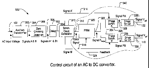
FIG. 5 is a block diagram of a control circuit of
an AC to DC converter in accordance with the present
invention;
FIG. 6 is a graph of signals generated by the
control circuit of the AC to DC converter of FIG. 5;
FIG. 7 is a circuit diagram of a zero voltage
crossing detector, a delay circuit and a synchronization
circuit of the control circuit shown in FIG. 5;
FIG. 8 is a graph of signals generated by the
circuits shown in FIG.7;
FIG. 9 is a circuit diagram of a zero voltage
crossing detector and a synchronization circuit with a
built-in delay (for a delay < 90 );
FIG. 10 is a graph of signals generated by the
circuits shown in FIG. 9;
FIG. 11 is a circuit diagram of a zero voltage
crossing detector and a synchronization circuit with a
built-in delay (for a delay > 90 );
FIG. 12 is a graph of signals generated by the
circuits shown in FIG. 11;
It will be noted that throughout the appended
drawings, like features are identified by like reference
numerals.
CA 02354454 2001-07-30
- g _
9-14628-3CA
DETAILED DESCRIPTION OF THE PREFERRED EMBODIMENT
The invention provides a pulse width modulation
control circuit for a high frequency series resonant AC/DC
converter.
FIG. 5 shows a block diagram of the control
circuit in accordance with the invention for the generation
of the appropriate gating signals, which are suitable for
controlling the FETs 108,116 of the circuit shown in
FIG. 1.
FIG. 5 is identical to FIG. 3, with the exception
that a delay circuit 502 has been inserted between the zero
crossing detector 306 and the synchronization circuit 310;
and the position of the first and second drivers 330,338
has been reversed. An input of the delay circuit 502 is
connected at 308 to the output of the zero crossing
detector 306 and an output of the delay circuit 502 is
connected at 504 to the input of the synchronization
circuit 310. The purpose of the delay circuit 502 is to
shift the gating signal 418 generated during the positive
cycle for the first FET 108 and the gating signal 420
generated during the negative cycle for the other FET 116.
In this way the zero crossing detection is pre-processed
and compensation for the effect of the circuit delays is
introduced.
FIG. 6 is a schematic diagram of the waveforms
generated by the control circuit shown in FIG. 5. The
auxiliary transformer 302 (FIG. 5) generates two
complementary voltage signals (FIG. 6) A 602 and B 604 at
its output. The zero-crossing detector circuit 306
generates signals A1 606 and B1 608. Signals A1 606 and
B1 608 correspond to positive half-cycles of signals A 602
and B 604 respectively. The delay circuit 502 (FIG. 5)
introduces a time delay (tdelay = T/2-tdpWM-tdDriver) , where T/2
(FIG. 4) is a time between zero-crossings of the AC input
CA 02354454 2001-07-30
- g _
9-14628-3CA
signal; tdPwM is the delay through the Pt-VM circuit; and,
tdDriver is the delay through the driver circuit . The
synchronization circuit 310 generates signals A' 610,
B' 612 and a clock signal 614. The rising edge of A' 610
and B' 612 generates the clock signal 614 at twice the
frequency of input signals A 602 and B 604. The clock
signal 614 is used to synchronize the PWM 320 at twice the
frequency of the AC input voltage 102. Based on the
feedback signal 324 (FIG. 5), the PWM 320 generates signal
PPwM 616, which is delayed with respect to the clock
signal 614 due to the internal delay tdPwM in the PWM 320.
First phase and second phase synchronizing circuits 326,334
generate signals PA 618 and PB 620 which are in phase and
frequency of the positive half-cycles of signals A 602 and
B 604 respectively, but are significantly delayed with
respect to the positive zero crossings of input signals
A 602 and B 604. Signals PA 618 and PB 620 are now used to
drive the second and first drivers 338,330. The internal
delays of these drivers 338,330 further delay the signals
PA 618 and PB 620 with respect to the clock signal 614, and
hence with respect to the zero crossings of the input
signals A 602 and B 604.
If the intentional delay is set according to the
above criteria, the gating signals Vgs2 622 and V9S1 624
output by the drivers 338,330 are in phase with the
respective positive half-cycles of input signals A 602 and
B 604. Gating signals generated in this way do not cause
cross-conduction between the two FETs 108,116, and provide
a maximum pulse width of about 180°.
There are a number of circuit configurations that
can be used to generate the delay tdeiay shown in FIG. 6.
Three potential circuit configurations are described below.
FIG. 7 shows a circuit diagram 700 for the zero
crossing detector 306, the delay circuit 502 and the
CA 02354454 2001-07-30
- 10 -
9-14628-3CA
synchronization circuit 310. The circuit 700 may be
implemented as an application specific integrated circuit
(ASIC), an integrated circuit (IC) or as discrete
components. The zero voltage crossing detector 306
comprises resistors RA1 710, RA2 714, zener diode ZA1 712,
and an AND logic gate GA1 716 for detecting zero crossings
of input voltage signal A 708. Resistors RBl 740, RB2 744,
zener diode ZB1 742 and an AND logic gate GB1 746 detect
zero crossings of input voltage signal B 738. The delay
circuit 502 includes a resistor RA3 722, a diode DA 720 and
a capacitor CA 724 for generating a ramp A2 726. Resistor
RB3 752, a diode DB 750 and a capacitor CB 754 for
generating a ramp B2 756. The synchronization circuit 310
comprises four NOR logic gates GA2 728A, GB2 728B, GCl 758,
GC2 762; one inverter GC3 764; a diode DC 768; a resistor
RC 770; and a capacitor CC 772 for generating appropriate
pulses for phase synchronization and clock generation.
FIG. 8 illustrates the waveforms generated by the
circuit shown in FIG. 7. When positive signal A 802 is
applied at the input 708 (FIG. 7) of the zero voltage
crossing detector, the voltage 806 at node ZA 713 follows
the positive input voltage whenever it is below a zener
voltage rating (VZ) of diode ZA1 712. It is clamped at VZ
whenever the voltage is above the voltage level VZ. The
voltage 806 at node ZA 713 is clamped at zero during the
negative half-cycle. If the zener voltage VZ is equal to a
threshold voltage (Vth) 814 of AND gate GA1 716, a
rectangular voltage pulse 810 is output at A1 718. The
rectangular voltage pulse 810 generates a ramp voltage 816
at node A2 726. Similarly, a ramp voltage signal 818 is
produced at node B2 756 corresponding to the positive half-
cycle of the input voltage signal B 804 on node 738. If
Vth is the threshold voltage 814 of NOR logic gates
GA2 728A and GB2 728B, the leading output states of both
the gates 728A,728B remain unchanged until the ramp
CA 02354454 2001-07-30
- 11 -
9-14628-3CA
voltages A2 816 and B2 818 exceed the threshold voltage
Vth. Therefore, the delay of the signals A2 816 and B2 818
can be adjusted by changing the slope of the ramp voltage
signals. The signals A' and B' generated by the
synchronization clock generator 310 (FIG. 5) are shown at
820 and 822. The gate signal generated by the NOR gate GC1
is shown at 824, and the gate signals C2,C3 respectively
generated by the inverter GC3 and input to the NOR gate GC2
are shown at 828 and 830. The logic gates GC1 758,
GC2 762, GC3 764 together with the diode-resistor-capacitor
network (DC 768, RC 770, CC 772) generates the clock
signal 832, shown in FIG.8.
FIG. 9 shows a circuit diagram 900 for an
alternate embodiment of the zero crossing detector 306 and
the synchronization circuit 310 with a built-in delay, when
the required delay time is less than one quarter of the
period (90°) of the AC input voltage 102. The zero voltage
crossing detector 306 comprises resistors RA1 906, RA2 908,
RA3 912, and a comparator CA 910 for detecting zero
crossings of input voltage signal A 902. Resistors
RB1 926, RB2 928, RB3 932 and comparator CB 930 detect zero
crossings of input voltage signal B 922. The
synchronization circuit 310 comprises four NOR logic gates
GA2 728A, GB2 728B, GC1 758, GC2 762; one inverter GC3 764;
a diode DC 768; a resistor RC 770; and a capacitor CC 772
for generating appropriate pulses for phase synchronization
and clock generation.
FIG. 10 illustrates the waveforms generated by the
circuit shown in FIG. 9. When positive signal A 1002 is
applied at the input 902 (FIG. 9) of the zero voltage
crossing detector, a rectangular voltage pulse 1006 is
output at A1 726. Similarly, when positive signal B 1004
is applied at the input 922 of the zero voltage crossing
detector, a rectangular voltage pulse 1008 is output at
B1 756. Therefore, the delay of the signals A1 1006 and
CA 02354454 2001-07-30
- 12 -
9-14628-3CA
B1 1008 can be adjusted by changing ratio of resistors
RA2 908 to RA3 912 and the ratio RB2 928 to RB3 932. The
signals A' and B' generated by the synchronization clock
generator 310 are shown at 1010 and 1012. The gate signal
generated by the NOR gate GC1 is shown at 1014, and the
signals C2,C3 respectively generated by the inverter GC3
and input to the NOR gate GC2 are shown at 1016 and 1018.
The logic gates GC1 758, GC2 762, GC3 764 together with the
diode-resistor-capacitor network (DC 768, RC 770, CC 772)
generates the clock signal 1020, shown in FIG.10.
FIG. 11 shows a circuit diagram 1100 of a further
alternate embodiment of the zero crossing detector 306 and
the synchronization circuit 310 with a built-in delay, when
the required delay time is greater than one quarter of the
period (90°) of the AC input voltage 102. The zero voltage
crossing detector 306 comprises resistors RA1 906, RA2 908,
RA3 912, and a comparator CA 910 for detecting zero
crossings of input voltage signal A 902. Resistors
RB1 926, RB2 928, RB3 932 and comparator CB 930 detect zero
crossings of input voltage signal B 922. The
synchronization circuit 310 comprises three NOR logic gates
GA2 728A, GB2 728B, GC2 762; one NAND gate 1102, one
inverter GC3 764; a diode DC 768; a resistor RC 770; and a
capacitor CC 772 for generating appropriate pulses for
phase synchronization and clock generation.
FIG. 12 illustrates the waveforms generated by the
circuit shown in FIG. 11. When positive signal A 1202 is
applied at the input 902 (FIG. 11) of the zero voltage
crossing detector, a rectangular voltage pulse 1206 is
output at A1 726. Similarly, when positive signal B 1204
is applied at the input 922 of the zero voltage crossing
detector, a rectangular voltage pulse 1208 is output at
B1 756. Therefore, the delay of the signals A1 1206 and
B1 1208 can be adjusted by changing ratio of resistors
RA2 908 to RA3 912 and the ratio RB2 928 to RB3 932. The
CA 02354454 2001-07-30
- 13 -
9-14628-3CA
signals A' and B' generated by the synchronization clock
generator 310 are shown at 1210 and 1212. The gate signal
generated by the NAND gate GCl 1102 is shown at 1214, and
the signals C2,C3 respectively generated by the inverter
GC3 and input to the NOR gate GC2 are shown at 1216
and 1218. The logic gates GCl 758, GC2 762, GC3 764
together with the diode-resistor-capacitor network (DC 768,
RC 770, CC 772) generates the clock signal 1220, shown in
FIG.10.
The invention therefore provides a control circuit
for a high frequency series resonant AC/DC converter that
has high conversion efficiency, little or no cross
conduction losses and increased effective pulse width.
The embodiments) of the invention described above
are intended to be exemplary only. The scope of the
invention is therefore intended to be limited solely by the
scope of the appended claims.