Note : Les descriptions sont présentées dans la langue officielle dans laquelle elles ont été soumises.
CA 02355447 2001-08-20
Doc. No. 10-373 CA CIP Patent
BI-DIRECTIONAL CROSS-CONNECT
FIELD OF THE INVENTION
The invention relates to optical devices including cross-connects, and in
particular to
optical devices including bi-directional cross-connects.
BACKGROUND OF THE INVENTION
For long-distance communications using optical fibers, amplifiers are used to
boost
signals along an optical path. Because amplifiers are one-way devices, two
fibers with associated
amplifiers are required for bi-directional communications using optical
fibers. One common
format for use with fiber optics communications is use of International
Telecommunications
Union (ITU) channels that define frequency spacing for multiplexed optical
signals.
Figure 1 illustrates one embodiment of bi-directional transmission of multiple
optical
channels using two optical fibers. Optical signals are transmitted from
multiple transmitting
devices 100 to multiple receiving devices 140 and from transmitting devices
150 (which can be
devices 140) to receiving devices 180 (which can be devices 100).
When transmitting from devices 100, the optical signals are multiplexed by
multiplexor
110 to generate a wavelength division multiplexed (WDM) or dense WDM (DWDM)
optical
signal. The WDM/DWDM optical signal is transmitted to amplifier 120, where the
signal is
strengthened and forwarded to amplifier 122. The sequence of amplification
continues as
necessary until the signal is received by demultiplexor 130. Amplification of
transmitted optical
signals is known in the art. Demultiplexor 130 demultiplexes the optical
signal and distributes
the signals to devices 140.
Optical signals transmitted from devices 150 to devices 180 are transmitted in
a similar
manner. The optical signals are multiplexed by multiplexor 190 to create a WDM
or DWDM
optical signal. The signal is transmitted via optical fiber to amplifiers 160
and 162 to
demultiplexor 170. Demultiplexor 170 demultiplexes the WDMlDWDM optical signal
and
CA 02355447 2001-08-20
Doc. No. 10-373 CA CIP Patent
distributes the optical signals to devices 180. The bi-directional network of
Figure 1 requires two
sets of multiplexors, demultiplexors, amplifiers, fibers and related
interconnections and is thus
inefficient network architecture.
Figure 2 illustrates one embodiment of bi-directional transmission of multiple
optical
channels using circulators and interleaving filters. In the architecture of
Figure 2 a first set of
optical frequencies (e.g. even ITU channels) are communicated in a first
direction and a second
set of optical frequencies (e.g. odd ITU channels) are communicated in the
opposite direction.
A WDM or DWDM signal is transmitted to circulator 210 via optical fiber 200.
Circulator 210 routes the optical signal to amplifier 220. Amplifier 220
amplifies the signal, and
filter 230 filters the amplified signal. Amplifier 225 further amplifies the
optical signal. The
filtering and amplification are performed as necessary based on, for example,
fiber length and/or
signal conditions. The optical signal is eventually routed to circulator 240.
Circulator 240 routes the optical signal from amplifier 225 to optical fiber
250, which
carries the optical signal to one or more receiving devices (e.g. a
demultiplexor). For optical
signals traveling in the opposite direction, optical fiber 250 carries signals
from a transmitting
device (e.g. a multiplexor) to circulator 240, which routes the optical signal
from fiber 250 to
amplifier 260. Amplifier 260, filter 270 and amplifier 265 amplify and filter
the optical signal as
necessary, and direct the optical signal to circulator 210.
Circulator 210 routes optical signals from amplifier 265 to optical fiber 200.
Optical
fiber 200 carries the optical signal to a receiving device (e.g. a
demultiplexor). The network
architecture of Figure 2, as with the network architecture of Figure 1,
requires two sets of
amplifiers. The network architecture of Figure 2 also requires two sets of
filters and at least two
circulators. The network of Figure 2 is can be more efficient than the network
architecture of
Figure 1; however, the network architecture of Figure 2 can be expensive to
build and to
maintain.
BRIEF DESCRIPTION OF THE DRAWINGS
2
CA 02355447 2001-08-20
Doc. No. 10-373 CA CIP Patent
The invention is illustrated by way of example, and not by way of limitation,
in the
figures of the accompanying drawings in which like reference numerals refer to
similar elements.
Figure 1 illustrates one embodiment of bi-directional transmission of multiple
optical
channels using two optical fibers.
Figure 2 illustrates one embodiment of bi-directional transmission of multiple
optical
channels using circulators and interleaving filters.
Figure 3 illustrates one embodiment of a block diagram of a wavelength
interleaving
cross-connect coupled to another optical device.
Figure 4 illustrates one embodiment of a block diagram of a wavelength
interleaving
cross-connect coupled to an add/drop device.
Figure 5 illustrates one embodiment of a wavelength interleaving cross-connect
having
multiple half wave plates and two birefringent elements.
Figure 6 illustrates one embodiment of a wavelength interleaving cross-connect
having
reflective elements to reflect optical signals through multiple half wave
plates and a birefringent
element.
Figures 7a and 7b illustrate one embodiment of a wavelength interleaving cross-
connect
having all four ports on a common side and a reflective element to reflect
optical signals through
multiple half wave plates and multiple birefringent elements.
Figure 8 illustrates one embodiment of a wavelength interleaving cross-connect
having a
polarization beam sputter and multiple etalons.
Figure 9 illustrates certain dimensions for one embodiment of a Michelson
phase shifter
cross-connect with a contact plate splitter.
3
CA 02355447 2001-08-20
Doc. No. 10-373 CA CIP Patent
Figure 10 illustrates one embodiment of a cross-connect using a multi-cavity
etalon.
Figure 11 is a block diagram representing the cross-connect of the present
invention in
combination with bi-directional isolators at the first and second ports for
feeding signals
traveling in opposite directions through an optical device in the same
direction.
Figure 12a and 12b illustrate an embodiment of the cross connect of Fig. 11.
Figure 13 is a polarization chart for the cross connect of Figs 12a and 12b.
DETAILED DESCRIPTION
Wavelength interleaving cross-connects are described in the following
description. For
purposes of explanation, numerous specific details are set forth in order to
provide a thorough
understanding of the invention. It will be apparent, however, to one skilled
in the art that the
invention can be practiced without these specific details. In other instances,
structures and
devices are shown in block diagram form in order to avoid obscuring the
invention.
Reference in the specification to "one embodiment" or "an embodiment" means
that a
particular feature, structure, or characteristic described in connection with
the embodiment is
included in at least one embodiment of the invention. The appearances of the
phrase "in one
embodiment" in various places in the specification are not necessarily all
referring to the same
embodiment.
Wavelength interleaving cross-connects pass a first optical signal including
channels
from a first set of optical frequencies in a first direction and a second
optical signal including a
second set of optical frequencies in a second direction. In one embodiment,
the first optical
signal, when input to a first input/output (I/O) port, is routed from the
first I/O port to a second
I/O port. The first optical signal, when input to a third I/O port, is routed
from the third port to a
fourth I/O port. The second optical signal, when input to the fourth I/O port,
is routed from the
fourth I/O port to the second I/O port. The second optical signal, when input
to the third I/O port,
CA 02355447 2001-08-20
Doc. No. 10-373 CA CIP Patent
is routed from the third I/O port to the first I/O port. Thus, by coupling an
optical device (e.g.,
amplifier, filter) between the second port and the third port, the optical
device can be used for bi-
directional communications thereby reducing the number of devices required for
a bi-directional
optical network architecture.
For simplicity of description the wavelength interleaving cross-connects
described herein
are described in terms of filtering and routing even and odd ITU channels;
however, the sets of
optical frequencies filtered and routed can be those other than ITU channels.
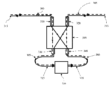
Figure 3 illustrates one embodiment of a block diagram of a wavelength
interleaving
cross-connect coupled to another optical device. One or more devices (not
shown in Figure 3)
transmit a first optical signal 305 having a first set of optical frequencies
(e.g., odd ITU
channels). One or more optical devices (not shown in Figure 3) receive a
second optical signal
315 having a second set of optical frequencies (e.g., even ITU channels). In
one embodiment,
odd channels 305 and even channels 315 are carried by a single optical fiber.
The transmitting
devices and the receiving devices can be the same device or different devices.
The optical fiber carrying odd channels 305 and even channels 315 is optically
coupled to
I/O port 310. In one embodiment, port 310 is a collimator assembly having a
graded index
(GRIN) lens to collimate the light . Other types of lenses can also be used,
or pre-collimated
light can be received. Port 310 is optically coupled to wavelength
interleaving cross-connect
300.
One or more devices (not shown in Figure 3) receive odd channels 305 and
transmit
even channels 315 via port 320 that is optical coupled to wavelength
interleaving cross-connect
300. The transmitting devices and the receiving devices can be the same device
or different
devices. In one embodiment, port 320 is a collimator assembly having a GRIN
lens to collimate
the light. Other types of lenses can also be used, or pre-collimated light can
be received.
I/O ports 330 and 340 are also optically coupled to wavelength interleaving
cross-connect
300. In one embodiment, ports 330 and 340 include collimator assemblies having
GRIN lenses
CA 02355447 2001-08-20
Doc. No. 10-373 CA CIP Patent
to collimate the light. Other types of lenses can also be used, or pre-
collimated light can be
received.
Optical device 350 is optically coupled between port 330 and 340. Optical
device 350
can be, for example, a channel equalizer, a filter, a repeater, an Erbium-
Doped Fiber Amplifier
(EDFA), a Semiconductor Optical Amplifier (SOA), a Rare Earth Doped Fiber
Amplifier
(REDFA) or other optical device.
The odd channels 305 (dashed line) input to wavelength interleaving cross-
connect 300
via port 310 and routed to port 330. The odd channels 305 are then input to
optical device 350.
The odd channels 305 as output by optical device 350 are carried to port 340
by an optical fiber
or other waveguide. The wavelength interleaving cross-connect 300 routes odd
channels 305
from the port 340 to the port 320.
The even channels 315 (solid line) are input to the wavelength interleaving
cross-connect
300 via the port 320 and routed to the port 330. The even channels 315 are
then carried to the
optical device 350. The even channels 315 as output by the optical device 350
are carried to the
port 340 by a suitable optical waveguide. The wavelength interleaving cross-
connect 300 routes
the even channels 315 from the port 340 to the port 310.
Because both the even channels 315 and the odd channels 305, which represent
bi-
directional communications, are routed from their respective input ports to
the port 330, a single
optical device (i.e., optical device 350) can be used for bi-directional
communications. The even
channels 315 and the odd channels 305 received from the optical device 350 via
the port 340 are
routed to the respective output ports to provide bi-directional
communications. Thus, the number
of optical devices (e.g. amplifiers), needed for bi-directional
communications, can be reduced by
as much as half.
Figure 4 illustrates one embodiment of a block diagram of a wavelength
interleaving
cross-connect coupled to an add/drop device. The wavelength interleaving cross-
connect 300
and the ports 310, 320, 330 and 340 operate in a similar manner as described
above with respect
to Figure 3.
6
CA 02355447 2001-08-20
Doc. No. 10-373 CA CIP Patent
An add/drop device 400 is coupled between the ports 330 and 340. The add/drop
device
400 receives the odd channels 305 and the even channels 315 from the port 330
of the
wavelength interleaving cross-connect 300. The add/drop device 400 includes
one or more
filters to filter one or more channels from the optical signals received. The
add/drop device 400
also receives the odd channels 410 and the even channels 420 from a device
(not shown in Figure
4) generating or transmitting the signals. One or more of the odd channels 410
and the even
channels 420 can be added to the even channels 305 and the odd channels 315 to
provide new
even channels 325 and odd channels 335 that are routed to the port 340 of the
wavelength
interleaving cross-connect 300. Dropped channels that have been filtered by
the add/drop device
400 are illustrated as odd channels 430 and even channels 440.
Figure 5 illustrates one embodiment of a wavelength interleaving cross-connect
having
multiple half wave plates and two birefringent elements. The elements of
Figure 5, with the
exception of I/O ports 310, 320, 330 and 340, represent one embodiment of
wavelength
interleaving cross connect 300.
In general, odd channels received via port 310 are directed to port 330, and
even channels
received via port 310 are directed to port 340. Odd channels received via port
320 are directed to
port 340, and even channels received via port 320 are directed to port 330. In
one embodiment,
to operate as described above with respect to Figures 3 and 4 odd channels are
input to port 310
and even channels are input to port 320. In an alternate embodiment, even
channels are input to
port 310 and odd channels are input to port 320.
The half wave plate 510, a first birefringent element 550, a half wave plate
515, a second
birefringent element 555, and a half wave plate 520 together operate as a
filtering element to
filter optical signals that pass therethrough. In one embodiment, the first
birefringent element
550 has an optical path length of L and the second birefringent element 555
has an optical path
length of 2L. In one embodiment, the filtering effect of half wave plates 510
(e.g. @ 22.5°),
515(e.g. @ 52.5°) and 520(e.g. @ 3.5°) and of birefringent
elements 550 and 555 provides a
comb function in both directions; however, other filtering functions can also
be provided.
7
CA 02355447 2001-08-20
Doc. No. 10-373 CA CIP Patent
Preferably, the polarization of a first set of frequencies (e.g. ITU even
channels) is rotated by 90°,
while the polarization of a second set of frequencies (e.g. ITU odd channels)
is unaffected. This
difference in response typically provides the opportunity for the odd and even
numbered channels
launched via the same input port to be directed to different ports; however,
in the present
invention it also enables the odd and even numbered channels launched via
different input ports
to be directed to the same output port. Of course, all of this depends on the
relative polarizations
of the odd and even channels when they are input into the device, and how
their polarizations are
otherwise manipulated within the system.
In one embodiment, the first and second birefringent elements 550 and 555 are
composed
of multiple birefringent crystals that are selected to provide improved
thermal stability over a
range of operating temperatures as compared to a single birefringent crystal.
In one embodiment,
one crystal is a TiOz crystal and a second crystal is a YVOQ crystal; however,
other crystal types
can also be used. Other birefringent assemblies can also be used, for example,
a single crystal
can be used if temperature stability is not important.
For the sake of example we will assume that the even numbered channels, are
input the
port 320 and the odd numbered channels are input the port 310. The components
of the optical
signal comprising even numbered channels launched via port 320 emerge from the
half wave
plate 520 in the orthogonal polarization state as when they entered half wave
plate 510, and
therefore pass through a polarization beam sputter 560 to a half wave plate
530 and to the port
330. Assuming that the port 330 is optically coupled to port 340 via an
optical device of some
kind, the even channels received via the port 340 will travel through the
cross-connect 300 in a
similar manner; however, a waveplate 540 is used to ensure that the
polarization of the even
channel components beginning the second pass is orthogonal to their
polarization after the first
pass. Accordingly, the even channels will get reflected by the prism 560 and
directed to the
waveplate 520. Once again, passage through the first and second birefringent
elements 550 and
555 results in a polarization rotation enabling the even channel components to
pass through the
prism 540 to the port 310.
8
CA 02355447 2001-08-20
Doc. No. 10-373 CA CIP Patent
Moreover, it is preferable for the signals that pass in a first direction
(e.g. left to right) to
exit the waveplate 520 with a polarization that is orthogonal to the signals
of the same frequency
set re-entering the waveplate 520 for a second pass in a second direction
(e.g. right to left). The
orthogonal relationship between the passes reduces, or even eliminates
chromatic dispersion for
signals that are passed from the port 310 to the port 330, through an optical
device to the port 340
and then to the port 320.
One of the components (e.g. the ordinary component) of the odd numbered
channels
received via the port 310 is directed to the filtering elements through a half
wave plate 500,
which ensures that the polarization of the odd channel components is
orthogonal to the
polarization of the even channel components launched via the port 320, and
that the components
of the odd numbered channels are passed directly through the polarization beam
sputter prism
540 to the waveplate 510. The polarization of the odd channels is unaffected
as a result of
passing through the filtering elements 550 and 555. Accordingly, the odd
channels are directed
to port 330 after passing directly through the polarization beam sputter 560.
The half wave plate
530 rotates the polarization of one of the odd channel components, whereby
they can be
combined in a walk-off crystal provided in the port 330.
The odd channels received via the port 340 are processed in a similar manner
as the odd
channel signals launched via the port 310, except that the waveplate 540
rotates the polarization
of one of the components thereof (e.g. extraordinary component) resulting in
the odd channel
components being reflected by the prism 560 and re-entering the waveplate 520
with a
polarization orthogonal to the polarization of the odd channel components
exiting the waveplate
520 after the first pass. As a result of passing through the first and second
filtering elements 550
and S55 a second time, the polarization of the odd channel components is again
unaffected,
which enables the odd channel components to be reflected by the prism 540 to
the port 320. As
with the even channels described above, an orthogonal relationship between
signals that pass in a
first direction and in a second direction can reduce, or even eliminate,
chromatic dispersion.
9
CA 02355447 2001-08-20
Doc. No. 10-373 CA CIP Patent
Figure 6 illustrates one embodiment of a wavelength interleaving cross-connect
having
reflective elements to reflect optical signals through multiple half wave
plates and a birefringent
element. The cross-connect of Figure 6 provides a similar functionality as the
cross-connect of
Figure 5; however, the cross-connect of Figure 6 passes signals though a
single birefringent
element multiple times rather than through multiple birefringent elements.
Signals, received via the port 310, are spatially separated into horizontal
and vertical
components by a walk-off crystal within the port 310. One of the components
passes through
half wave plate 605 (e.g. extraordinary component), whereby when entering the
polarization
beam splitter prism 540, both components have the same polarization. Moreover,
the waveplate
605 ensures that the signals coming from the port 310 have a state of
polarization that enables
them to pass directly through the polarization beam sputter 540.
Signals, received via the port 320, are spatially separated into horizontal
and vertical
components by a walk-off crystal within the port 320. One of the components
(e.g. ordinary
component) passes through half wave plate 600, whereby when entering the
polarization beam
sputter prism 540, both components have the same polarization, which is
orthogonal to the
polarization of the aforementioned components from the port 310. Moreover, the
waveplate 600
ensures that the signals coming from the port 320 have a state of polarization
that enables them
to be reflected by the polarization beam sputter 540. Subsequently, all of the
components pass
through a hole in a reflective element 650. In one embodiment, reflective
element 650 is a
reflective prism; however, other components could also be used.
Reflective elements 650 and 655 reflect the signals through half wave plates
610, 620,
625 and 630, through a polarizer 615, and through a birefringent element 660 a
plurality of times.
The polarization of the components of the odd channel signals is unaffected by
the multiple
passes through the single birefringent element 660, while the polarization of
the even channel
signals is rotated by 90°. Accordingly, the odd channel components
launched via the port 310
and the even channel components launched via the port 320 pass directly
through the polarization
beam sputter prism 560 to the port 330. Prior to entering the port 330 one of
the components
CA 02355447 2001-08-20
Doc. No. 10-373 CA CIP Patent
passes through half wave plate 640, which re-orients the one component
orthogonal to the other.
Alternatively, odd channel components launched via the port 320 and even
channel components
launched via the port 310 get reflected by the prism 560 to the port 340. As
above, prior to
entering the port 340 one of the components passes through half wave plate
635, which re-orients
the one component orthogonal to the other The azimuth angles of the half wave
plates and the
birefringent element are chosen to provide the desired filtering
functionality. Design of such
filters is known in the art.
In one embodiment, birefringent element 660 is composed of multiple
birefringent
crystals that are selected to provide improved thermal stability over a range
of operating
temperatures as compared to a single birefringent crystal. In one embodiment,
one crystal is a
TiOz crystal and a second crystal is a YVOQ crystal; however, other crystal
types can also be used.
Other birefringent assemblies can also be used, for example, a single crystal
can be used if
temperature stability is not important.
Assuming that the device of Figure 6 defines the cross connect 300 of Figure
3, odd
channels launched via the port 310 exit via the port 330, and subsequently are
received via port
340. The recently processed odd channels are passed through half wave plate
635, thereby
ensuring that the polarization of both of the components is the same but
orthogonal to the
polarization of the odd channels exiting the waveplate 620. Accordingly, the
polarization beam
splitter 560 directs the odd channel components though the half wave plates,
the polarizer and the
birefringent element for a second time. After filtering, the odd channels, the
polarization of
which remains the same, are passed to port 320 through polarization beam
sputter 540.
Even channels are routed in a similar manner from the port 320 to the port 330
and from
the port 340 to the port 310, taking into account that the polarization of
even channel signals is
rotated by 90° each time they pass between waveplates 610 and 620. In
one embodiment,
signals that pass in a first direction (e.g., left to right) have a
polarization that is orthogonal to
signals of the same frequency set that pass in a second direction (e.g., right
to left). The
orthogonal relationship between the passes reduces, or even eliminates,
chromatic dispersion for
11
CA 02355447 2001-08-20
Doc. No. 10-373 CA CIP Patent
signals that are passed from port 310 to port 330, through and optical device
to port 340 and then
to port 320.
Figures 7a and 7b illustrate one embodiment of a wavelength interleaving cross-
connect
having all four ports on a common side and a reflective element to reflect
optical signals through
multiple half wave plates and multiple birefringent elements. The cross-
connect of Figure 7
provides a similar functionality as the cross-connect of Figures 5; however,
the cross-connect of
Figure 7 passes signals though multiple birefringent elements to a mirror and
then back through
the multiple birefringent elements. This arrangement ensures that the
transmission between each
set of ports is chromatic dispersion free.
An optical signal carrying odd channels is received via port 310, and is
spatially separated
into orthogonal sub-beams by a walk-off crystal provided therein. One of the
sub-beams passes
through a half wave plate 710, which ensures both sub-beams have the same
polarization for
passage through the device, e.g. horizontal. Both components enter a prism
725, which routes
the signals through a half wave plate 730, a first birefringent element 735, a
half wave plate 740,
a second birefringent element 745 and a half wave plate 750. In a preferred
embodiment, the
first birefringent element 735 has an optical path length of L, and the second
birefringent element
745 has an optical path length of 2L; however, other optical path lengths can
also be used. The
combination of the half wave plates 730, 740 and 750, and the first and second
birefringent
elements 735 and 745 operate to filter the optical signal, as desired.
Preferably, the assembly
also rotates the polarization of one of the subsets of channels (e.g. the even
numbered ITU
channels), while having no cumulative effect on the other subset of channels
(e.g. the odd
numbered ITU channels).
After emerging from the half wave plate 750, the odd channel components, still
having
their original polarization (horizontal), pass through walk-off crystal 755 to
a quarter wave plate
760 and a mirror 770, which combine to direct the sub-beams with the first
polarization from a
lower level containing the port 310 to a middle level containing the ports 330
and 340. At this
point, even numbered ITU wavelengths would have the second polarization, and
get spilled off
12
CA 02355447 2001-08-20
Doc. No. 10-373 CA CIP Patent
by the walk-off crystal 755. The quarter wave plate 760 is positioned to
intersect the sub-beams
and provide a polarization rotation of 45° for each pass therethrough.
The mirror 770 reflects the
optical signals back through quarter wave plate 760 for a second time
resulting in a full 90°
rotation of the sub-beams to the second polarization. Accordingly, the walk-
off crystal 755
passes the sub-beams, during their second pass, upwardly towards the middle
level. The sub-
beams pass through to the half wave plate 750, the second birefringent element
745, the half
wave plate 740, the first birefringent element 735 and the half wave plate 730
for a second pass
with a polarization (e.g. vertical) orthogonal to the polarization during the
first pass. The sub-
beams pass through a polarization beam splitting prism 727, which passes light
having vertical
polarization to the port 330. Between the ports 330 and 340, the sub-beams are
passed through
an optical device of some kind, such as an amplifier or an add/drop
multiplexer.
One of the odd channel sub-beams received via port 340 are passed through a
half wave
plate 700 to ensure both sub-beams have the original polarization
(horizontal). Accordingly,
both of the sub-beams are reflected by the polarization beams splitting prism
720 and through the
half wave plate 730, the first birefringent element 735, the half wave plate
740, the second
birefringent element 745, and the half wave plate 750 to the walk-off crystal
755. At this point,
because the odd channel sub-beams still have their original polarization, the
walk-off crystal 755
directs the sub-beams from the middle level up to the higher level containing
the port 320.
Again, the sub-beams pass through the quarter wave plate 760 to mirror 770,
which reflects the
sub-beams back through the quarter wave plate 760. As a result of the double
pass through the
quarter wave plate 760 the polarization of the sub-beams is rotated from their
original
polarization to an orthogonal polarization (vertical). The signals are then
reflected back
upwardly through the walk-off crystal 755 to the higher level and to the
waveplate 750, the
second birefringent element 745, the waveplate 740, the first birefringent
element 745, and the
waveplate 730. A prism 720, on the third level, reflects the sub-beams to the
port 320. One of
the sub-beams passes through a half wave plate 715, which enables the sub-
beams containing the
odd numbered channels to be combined and output the port 320.
13
CA 02355447 2001-08-20
Doc. No. 10-373 CA CIP Patent
The even channels are routed in a similar manner from port 320 to port 330 and
from port
340 to port 310. The even channel sub-beams are launched via the port 320 on
the upper level,
and the half wave plate 715 ensures that both sub-beams have the same
polarization (e.g.
horizontal). Passage through the birefringent elements and associated
waveplates results in a 90°
rotation from the original polarization to an orthogonal polarization
(vertical). Accordingly, the
even channel sub-beams pass downwardly through the walk-off crystal 755 to the
middle level
before intersecting the quarter wave plate 760 and mirror 770. The quarter
wave plate 760
rotates the even channel sub-beams back to their original polarization
(horizontal), whereby the
walk-off crystal directs them back along the middle level during the second
pass therethrough.
Again passage through the birefringent elements and associated waveplates
results in another 90°
rotation from the original polarization to an orthogonal polarization
(vertical). As a result, the
even channel sub-beams also pass directly through the polarization beams
splitting prism 727 to
the port 330. As above, when the even channel sub-beams re-enter the device
via the port 340,
the half wave plate 700 ensures that both sub-beams have the original
polarization (horizontal).
However, the polarization of the even channel sub-beams again is effected by
passage through
the birefringent elements and associated waveplates, which rotates their
polarization from their
original polarization to an orthogonal polarization (vertical). Accordingly,
the walk-off crystal
755 passes the even channel sub-beams downwardly therethrough to the lower
level and to the
quarter wave plate 760 and mirror 770. The quarter wave plate 760 rotates the
polarization of the
sub-beams back to their original polarization (horizontal) enabling the walk-
off crystal 755 to
direct them back along the lower level. After yet another polarization
rotation by the birefringent
elements 735 and 745, the even channel sub-beams are directed to the port 310
for
recombination, with the help of the waveplate 710.
In one embodiment, signals that pass in a first direction (e.g., left to
right) have a
polarization that is orthogonal to signals of the same frequency set that pass
in a second direction
(e.g., right to left). The orthogonal relationship between the passes reduces,
or even eliminates,
74
CA 02355447 2001-08-20
Doc. No. 10-373 CA CIP Patent
chromatic dispersion for signals that are passed from port 310 to port 330,
through and optical
device to port 340 and then to port 320 or vice versa.
Figure 8 illustrates one embodiment of a wavelength interleaving cross-connect
having a
beam sputter and multiple etalons. The cross-connect described includes a
Fabry-Perot phase
shifter (FPPS) providing phase shifting for an optical signal, and a Fabry-
Perot etalon in a
Michelson arrangement. The combination of the FPPS and the etalon provide
sufficient
passband width and isolation to operate as an interleaver/deinterleaver. A
similar device is
disclosed in United States Patent No. 6,169,626 issued January 2, 2001 to Chen
et al, which is
incorporated herein by reference.
In one embodiment, the components of cross-connect 300 are held in optical
contact by
atomic force rather than epoxy; however, epoxy can also be used. In order to
maintain optical
contact by atomic force, the thickness of each glass plate should be
consistent within a
predetermined tolerance. In one embodiment the thickness tolerance for each
plate is 1.0 pm;
however, other tolerances can also be used.
Because of the flatness of the components of the cross-connect 300, by
abutting the
components to each other, contact is maintained by atomic forces. In one
embodiment, use of
atomic force to maintain optical contact allows material matching to within
1.0 ~tm. As
mentioned above, optical contact by atomic force also provides better thermal
performance
compared to use of epoxy to assemble optical components.
The beam splitter cube 800 splits the optical signal into a first sub-beam and
a second
sub-beam. In one embodiment, beam sputter cube 800 splits the beam evenly such
that each
etalon receives a 50% strength version of the input signal. In other words,
beam sputter cube 800
is a 50/50 beam sputter. Other types of beam sputters can also be used.
Because a precise 50/50
beam sputter is difficult to manufacture, other beam splitting ratios can also
be used. In one
embodiment, the two crystals of beam sputter 800 are maintained in optical
contact by atomic
force.
CA 02355447 2001-08-20
Doc. No. 10-373 CA CIP Patent
Assuming a 50/50 beam split by beam sputter cube 800, the first sub-beam is
directed to
etalon 830 and the second sub-beam is directed to FPPS 850. In one embodiment,
front
reflective material of etalon 830 reflects 0% to 10% of the signal directed to
etalon 830 by beam
sputter cube 800. In one embodiment, the gap between the front reflective
material and the back
reflective material is 0.75 mm; however, other gap sizes can also be used. The
back reflective
material reflects 90% to 100% of the signal passed by the front reflective
material.
In one embodiment, etalon 830 is coupled to beam splitter cube 800 by optical
contact. In
such an embodiment, the gap between etalon 830 and beam sputter cube 800 can
be less than 1.0
pm. In an alternate embodiment, etalon 830 is coupled to beam splitter cube
800 with epoxy;
however, the gap between etalon 830 and beam splitter cube 800 is generally
larger than when
coupled by atomic force. In one embodiment, etalon 830 includes a tuning plate
(not shown in
Figure 8). The tuning plate provides cross-connect 300 with fine resolution
(e.g., 10 nm or less).
The tuning plate provides fine tuning capability by changing the effective
optical path length
through etalon 830.
The second sub-beam is passed beam sputter cube 800 to FPPS 850. In one
embodiment,
the front reflective material reflects 15% to 20% of the second sub-beam
directed to FPPS 540 by
beam sputter cube 800. In one embodiment the gap between the front reflective
material and the
back reflective material is 1.5 mm; however, other gap sizes can also be used.
The back
reflective material reflects 90% to 100% of the signal passed by the front
reflective material. The
reflected second sub-beam is directed to the beam sputter cube interface and
reflected to the
appropriate port. In one embodiment, FPPS 850 is coupled to beam sputter cube
800 by atomic
force. In an alternate embodiment, FPPS 850 is coupled to beam splitter cube
800 with epoxy.
Etalon 830 provides a linear phase difference and a sinusoidal transfer
function for the
first sub-beam. FPPS 850 provides a non-linear phase response with slight
attenuation for the
second sub-beam. The phase and intensity response of etalon 830 and FPPS 850
cause
constructive and destructive light interference at the beam sputter cube
interface. The
frequencies for which constructive light interference occurs are passed at or
near full intensity.
16
CA 02355447 2001-08-20
Doc. No. 10-373 CA CIP Patent
The frequencies, for which destructive light interference occurs, results in
attenuation of the
optical signal.
This device is effectively the same as the aforementioned cross connects,
whereby odd
channels input the port 310 and even channels input the port 320 get output
the port 330, while
odd and even channels input the port 340 get output the ports 320 and 310,
respectively.
Figure 9 illustrates certain dimensions for one embodiment of a Michelson
phase shifter
cross-connect in which the ports 310, 320, 330 and 340 are optically coupled
with a contact plate
splitter 900. In one embodiment, the air gap dimensions, the phase matching
parameters and the
design parameters are the same for the interleaver with the contact plate as
with the interleaver
with the beam splitter with the following exception:
L, ~ LZ ~ O.S,um for a plate splitter embodiment.
In general, the cross-connect of Figure 9 operates in a similar manner as the
beam splitter
cube cross-connect described above. In one embodiment, plate sputter 900 is a
50/50 beam
sputter; however, other plate sputters can be used. In one embodiment crystals
902 and 904 are
silica; however, other materials can also be used.
In one embodiment, FPPS 910 and etalon 920 are coupled to the contact plate
sputter by
atomic force. Coupling with atomic force allows the gaps between FPPS 910 and
the contact
plate splitter and between etalon 920 and the contact plate sputter to be less
than 1.0 Vim. In an
alternate embodiment, FPPS 910 and etalon 920 are coupled to the contact plate
sputter by
epoxy. As mentioned above, coupling with atomic force improves both thermal
and optical
performance.
The optical signal passes through crystal 902 to plate splitter 900. In one
embodiment,
plate sputter passes 50% of the intensity of the optical signal and reflects
the other 50% of the
intensity of the optical signal. Thus, plate sputter 900 is a 50/50 plate
sputter; however, other
plate splitters can also be used.
The reflected optical signal passes through crystal 902 to FPPS 910. A phase-
shifted
version of the optical signal is reflected back to plate sputter 900. The
transmitted optical signal
17
CA 02355447 2001-08-20
Doc. No. 10-373 CA CIP Patent
passes through crystal 904 to etalon 920. A version of the optical signal
having a linear phase
difference is reflected back to plate sputter 900.
At plate sputter 900, the reflected signals converge and, through constructive
and
destructive interference, are separated into even and odd channels. In one
embodiment, tuning
plate 960 is used to fine-tune the phase characteristics of the cross-connect.
In one embodiment,
a ~0.01 ° adjustment to tuning plate 960 corresponds to a ~10 nm phase
distance.
Figure 10 illustrates one embodiment of a cross-connect having a multi-cavity
etalon
optical comb filter optically coupled to the ports 310, 320, 330 and 340. In
order to provide
filtering that is sufficiently accurate to provide comb-filtering
functionality for International
Telecommunications Union (ITU) channel spacing, the thickness of each glass
plate should be
consistent within a predetermined tolerance. In one embodiment the thickness
tolerance for each
plate is 1.0 ~tm; however, other tolerances can also be used.
In general, the comb filter cross-connect 300 includes glass plates 1010, 1020
and 1030.
The comb filter cross-connect 300 also includes reflective coatings/materials
1040, 1050, 1060
and 1070. In one embodiment, the components of the comb filter cross-connect
300 are held in
optical contact by atomic force rather than epoxy; however, epoxy can also be
used. Because of
the flatness of the components of the comb filter cross-connect 300, by
abutting the components
to each other, contact is maintained by atomic forces.
In one embodiment, the glass plates 1010, 1020 and 1030 are 0.5 mm thick for
100 GHz
spaced input signals, 1.0 mm thick for 50 GHz spaced input signals, and 0.25
mm thick for 200
GHz spaced input signals. Other plate thicknesses can be used, for example,
for other input
signal spacings.
In one embodiment, reflective coatings/materials 1040 and 1070 have
approximately the
same reflectivity, and reflective coatings/materials 1050 and 1060 have
approximately the same
reflectivity, which is different than the reflectivity of coatings/materials
1040 and 1070. In one
embodiment, the reflectivity of coatings/materials 1040 and 1070 is in the
range of 20% to 30%
reflective, and the reflectivity of coatings/materials 1050 and 1060 is in the
range of 60% to 70%
18
CA 02355447 2001-08-20
Doc. No. 10-373 CA CIP Patent
reflective. Other reflectivities can also be used, and mufti-cavity etalons
having more than three
plates can also be used.
This device is effectively the same as the aforementioned cross connects,
whereby odd
channels input the port 310 and even channels input the port 320 get output
the port 330, while
odd and even channels input the port 340 get output the ports 320 and 310,
respectively.
Figure 11 schematically illustrates the bi-directional cross connect 300
according to the
present invention in combination with a pair of bi-directional isolators 1110
and 1120 forming a
uni-directional cross connect with double stage spectral isolation for use
with an optical device
1150, e.g. an amplifier. The bi-directional isolators 1110 and 1120 are more
thoroughly
described in co-pending United States Patent Application No 09/558,848 filed
April 27, 2000,
which is incorporated herein by reference.
With reference to Figures 12a and 12b, a cross connect capable of fulfilling
the scheme
illustrated in Figure 11 includes ports 1201, 1202, 1203 and 1204. Each port
includes a lens
1210 fixed to a ferrule 1215, which surrounds a fiber 1220. To ensure that the
device is
polarization independent, each port also includes a walk-off crystal 1225 for
dividing the input
beams into orthogonally polarized sub-beams and/or for combining orthogonally
polarized sub-
beams for output. A half wave plate 1230 is provided for rotating the
polarization of one of the
sub-beams launched via the port 1201, so that both sub-beams have a first
polarization (e.g.
vertical). A half wave plate 1235 is provided for rotating the polarization of
one of the sub-
beams launched via the port 1202, so that both sub-beams have a second
polarization (e.g.
horizontal). Another half wave plate 1240 is provided at port 1203 for
rotating the polarization
of one of the outgoing sub-beams, so that the pair of outgoing sub-beams can
be combined by
walk-off crystal 1225. The port 1204 also includes a half wave plate 1245 for
rotating one of the
sub-beams of the light received via the optical device 1150 (Fig. 11 ) so that
both of the sub-
beams have the first polarization (e.g. vertical).
The remainder of the description of the device of Figure 12 will be made with
reference
to Figure 13. A signal comprised of wavelengths from a first set of
wavelengths (e.g. even-
19
CA 02355447 2001-08-20
Doc. No. 10-373 CA CIP Patent
numbered ITU channels), along with some unwanted wavelengths from a second set
of
wavelengths (e.g. odd-numbered ITU channels) is input the port 1201, and due
to the walk-off
crystal 1225 and the half wave plate 1230, becomes a first polarization (e.g.
vertical). The signal
passes through a non-reciprocal rotator 1250 comprised of a half wave plate
1251 and a Faraday
rotator 1252. In the forward direction, i.e. left to right, the polarization
rotations caused by the
half wave plate 1251 and the Faraday rotator 1252 cancel each other out, and
therefore have no
effect on the polarization of the sub-beams in question. Subsequently, the sub-
beams pass
through a birefringent assembly 1255, preferably including a first
birefringent element of length
L and a second birefringent element of length 2L. The birefringent assembly
selectively rotates
the polarization of the second set of wavelengths (e.g. the odd-numbered ITU
channels), while
having no cumulative effect on the polarization of the first set of
wavelengths (e.g. the even-
numbered ITU channels). As a result, the polarization of the unwanted
wavelengths from the
second set of wavelengths in the signal is rotated, while the polarization of
the wavelengths from
the first set of wavelengths remains the same. This difference in polarization
enables the
unwanted wavelengths to be directed away from the remainder of the signal in a
walk-off crystal
1260. The portion of the signal including wavelengths from the first set of
wavelengths, which
remained the first polarization (e.g. vertical), is passed directly through
the walk-off crystal 1260,
while the remainder is spilled off at an angle. The remaining signal is passed
through another
birefringent assembly 1265, preferably including a first birefringent element
of length L and a
second birefringent element of length 2L, which also has no effect on the
polarization of the first
set of wavelengths (e.g. even ITU channels). A walk-off crystal 1270 directs
the sub-beams
having the first polarization (e.g. vertical) to the port 1203.
Similarly, a signal comprising wavelengths from the second set of wavelengths
(e.g. odd-
numbered ITU channels), along with unwanted wavelengths from the first set of
wavelengths, is
input the port 1202 resulting in two sub-beams with the second polarization
(e.g. horizontal).
These sub-beams get directed by prism 1272 through the non-reciprocal rotator
1250, which has
no effect on the polarization thereof, to the birefringent assembly 1255,
which rotates the
CA 02355447 2001-08-20
Doc. No. 10-373 CA CIP Patent
polarization of the wavelengths in the second set of wavelengths by 90°
from the second
polarization to the first polarization (e.g. to vertical), while leaving the
polarization of the
wavelengths in the first set of wavelengths unaffected, e.g. horizontal. A
half wave plate 1280 is
positioned in the path of the sub-beams from the port 1202 for rotating the
polarization of all of
the wavelengths by 90°, thereby making the unwanted wavelengths the
first polarization (e.g.
vertical), while making the remainder of the signal the second polarization
(e.g. horizontal).
Accordingly, the walk-off crystal 1260 spills off the unwanted light and
directs the wavelengths
from the second set of wavelengths with the second polarization through the
birefringent
assembly 1265, which rotates the polarization thereof from the second
polarization to the first
polarization (e.g. vertical). Since the sub-beams have the first polarization,
the walk-off crystal
1270 directs them to the port 1203, as with the aforementioned sub-beams from
the first set of
wavelengths input the port 1201.
Assuming that both sets of sub-beams, which were output the port 1203, get
passed
through an optical device 1150 (Fig. 11 ) and input the port 1204, we will
describe their routes
simultaneously will reference to the second last flow chart at the bottom of
Figure 13. Passage
through the port 1204 results in either signal becoming two sub-beams with the
second
polarization (e.g. horizontal). To ensure minimal chromatic dispersion the
polarization of the
sub-beams re-entering the birefringent assembly 1265 is orthogonal to the
polarization of the
sub-beams exiting the birefringent assembly 1265. The sub-beams are directed
through the walk-
off crystal 1270 to the birefringent assembly 1265. Passage through the
birefringent assembly
1265 results in the polarization of the wavelengths in the second set of
wavelengths (e.g. odd
channels) being rotated to the first polarization (e.g. vertical), while the
polarization of the first
set of wavelengths is unaffected. Accordingly, the sub-beams including
wavelengths from the
second set of wavelengths is passed directly through the walk-off crystal 1260
to the birefringent
assembly, while the sub-beams including wavelengths from the first set of
wavelengths is
directed through the walk-off crystal 1260 along a different path to the half
wave plate 1280.
The half wave plate 1280 rotates the polarization of the sub-beams including
wavelengths from
21
CA 02355447 2001-08-20
Doc. No. 10-373 CA CIP Patent
the first set of wavelengths (e.g. even channels), whereby both sets of sub-
beams have the first
polarization entering the birefringent assembly 1255. Again, the birefringent
assembly 1255
rotates the polarization of the second set of wavelengths, while having no
cumulative effect on
the polarization of the first set of wavelengths. In this direction, i.e.
right to left, the non-
reciprocal rotator 1250 rotates the polarization of all of the sub-beams by
90°. This last rotation
ensures that the sub-beams have the proper polarization to be combined in the
appropriate ports
and output. If the polarization is not correct the sub-beams will be spilled
off, as in the last flow
chart, which charts the polarization of sub-beams launched into port 1203.
In the preferred embodiment illustrated in Figures 12 a and 12b, the bi-
directional
isolators 1110 and 1120 of Figure 11 are combined into a single unit including
the non-reciprocal
rotator 1250 and the birefringent assembly 1255.
In the foregoing specification, the invention has been described with
reference to specific
embodiments thereof. It will, however, be evident that various modifications
and changes can be
made thereto without departing from the broader spirit and scope of the
invention. The
specification and drawings are, accordingly, to be regarded in an illustrative
rather than a
restrictive sense.
22