Note : Les descriptions sont présentées dans la langue officielle dans laquelle elles ont été soumises.
CA 02356415 2001-08-30
OOLUC0253E;PP
Lucent Technologies
Radio system, antenna arrangement and polarization
modulator for generating a transmit signal with
changing polarization
Description
The invention relates to a radio system, in
particular a mobile radio system, with a plurality of
base stations, each base station being assigned at
least one dual-polarized antenna. Furthermore, the
invention relates to an antenna arrangernent, in
particular for operation with a-base station of a radio
system, and a polarization modulator for use in such a
radio system.
The recent sharp increase in the number of
mobile radio subscribers and the provision of new
services in mobile radio have caused mobile radio
networks, such as the GSM network for example, to
approach the limits of their capacity. As is known, in
the GSM network, traffic channels are used for the
transmission of user data and signalling channels are
used for the control and management of a mobile radio
network. However, the signalling load in a mobile
radio network is very high, since information has to J~e
constantly exchanged over the air interface, even whf=_n
no connection has been set up between a base station
and a mobile station. An important signalling channel
is represented here by the so-called broadcast. control
channel, also known as the BCCH channel, over which fc~r
example radio channel configurations, synchronizing
information and identifications for registration a==a
sent to all the mobile stations of a cell. Such a BC(;H
channel may take up as much as half of the availab_Le
frequency spectrum of a cell, which is then of course
no longer available for traffic channels. To allow
CA 02356415 2001-08-30
- 2 -
better utilization of the spectrum reserved for a cell,
it is generally known to subject the individual traffic
channels when need be to a frequency hopping process,
in which the carrier frequency for a traffic channel is
changed at a predetermined regular rate. The frequency
hopping process cannot be used, however, for a BCCH
channel, since the BCCH channel is required for
measurements of the receiving field strength and
selection of the strongest cell. This has the result
that the distance between cells in which the same BCCH
carrier frequency is being used is much greater than
the distance between cells in which the same traffic
carrier frequency is being used. For example, the
cluster size for a BCCH channel of a GSM network is 12
to 21 cells, whereas for traffic channels a cluster
size of 3 to 9 cells is entirely adequate. The cluster
size is understood here as meaning the number of cells
among which the available frequencies are divided.
However, there have previously been no proposed
ways of making more efficient use of the a~railabl~=_
carrier frequencies for signalling channels in thf~
manner possible with the aid of the frequency hoppin~~
process for traffic channels.
The invention is therefore based on the object
of providing a radio system, an antenna arrangement and
a polarization modulator with which the frequencies
available for a radio network can be used more
efficiently, in particular with regard to signalling
channels, and consequently the cluster size of a radio
network can be reduced.
The basic concept of the invention ins to be
seen in the idea of using instead of the frequency
hopping process a so-called polarization hopping
process, with which the polarization state of ~~
transmit signal can be changed, preferably on ~i
cyclical basis. If polarization hopping is used for
BCCH channels, the cluster size can be signif=icantly
reduced and consequently the frequency spectrum
CA 02356415 2001-08-30
- 3 -
available in a cell can be assigned to a greater number
of traffic channels.
This is so because, as is known, the frequency
hopping process has the result that channels with
different mid frequencies have fading responses that
are independent of one another as long as the frequency
hops are large enough. This response is obtained even
if, instead of frequency hops, different polarization
states are used for a radio link. For example, a data
block of a GSM network comprises four data bursts, it
being intended for the fading response of the channels
for each of the four bursts to be independent: of- one
another. This condition can therefore be satisfied
both by different frequency hops and by different
changes of the polarization states.
The invention achieves the object mentioned
above in the first instance by the features of Claim 1.
The latter specifies the provision of a radio
system, in particular a GSM mobile radio system, which
comprises a plurality of base stations, which have at
least one transmitter and one receiver, with each base
station being assigned at least one dual-polarized
antenna. The dual-polarized antenna may be a cross
polarized antenna. According to the invention, the
dual-polarized antenna is assigned a polarization
modulator for changing at predetermined points in time
the polarization state of a transmit signal. to be
transmitted .
Advantageous developments are the subject of
the dependent claims.
To allow already existing base stations to
continue to be used, the dual-polarized antenna and the
polarization modulator together form a module which can
be connected to the base station.
The polarization modulator expediently
activates the dual-polarized antenna with the transmit
signal to be transmitted in such a way that the
polarization of the signal to be transmitted changes on
CA 02356415 2001-08-30
-
a cyclical basis between typically four different=
polarization states.
If a GSM mobile radio system is concerned, in
which the signals are transmitted in so-called TDM~~
frames with eight time slots, the points in time fo~_
changing the polarization state are determined by a
clock generator in dependence on the TDMA frame~> or the
time slots within a TDMA frame.
Since the dual-polarized antenna is used both
for the transmitting direction and for the receiving
direction, transmitter/receiver filters are provided,
in a manner known per se, at corresponding locations.
The object specified above is likewise achieved
by the features of Claim 8.
The latter specifies the provision of an
antenna arrangement with at least one dual-polarized
antenna, which is respectively assigned a polarization
modulator for changing at predetermined points in time
the polarization state of a transmit signal to be
transmitted.
Advantageous developments of the antenna.
arrangement are the subject of the dependent claims.
The object is further achieved by the feature,
of Claim 12.
The latter defines a polarization modulator for
use in a radio system, said modulator generating a
plurality of polarization states for a transmit signal
in dependence on an applied clock signal.
The invention is explained in more detail below
on the basis of an exemplary embodiment in conjunction
with the attached drawings, in which:
Figure 1 shows the block diagram of a base
station to which an antenna arrangement according to
the invention is assigned, and
Figures 2a-d respectively show an equivalent
circuit of the polarization modulator shown in Figure 1
for four different polarization states.
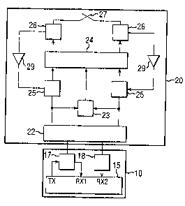
Schematically represented in Figure 1 is a base
station, for example of a GSM mobile radio network,
CA 02356415 2001-08-30
- 5 -
denoted generally by 10. The base station 10 has, in a
way known per se, inter alia, a transceiver 15, which
comprises for example a transmitter TX and two
receivers RX1, RX2 for diversity reception. Of course,
further transceivers may be implemented in the bare
station. In the present example, the transmitter TX
and the receiver RX1 are connected to a duplexer 17 for
separating the transmitting direction and receiving
direction. The receiver RX2 is connected to a bandpa:~s
filter 18.
Figure 1 also shows an antenna arrangement.,
denoted generally by 20, which has a -d. c. diplexing
filter and a power supply device 22. The d.c.
diplexing filter ensures that only the RF transmit
power is allowed through by the transceiver 15. The
antenna arrangement. 20 is designed as a separate device
from the base station 10 and is connected via the d.c.
diplexing filter and power supply device 22 to the
duplexer 17 and the bandpass filter 18 of the bay>e
station 10. A clock-recovery and control circuit 23
implemented in the antenna arrangement 20 has two
inputs, which are connected to the d.c. diplexing
filter and supply device 22. The output of the clock:-
recovery and control circuit 23 is connected to a
polarization modulator 24, which is explained i.n
further detail below. The clock-recovery and control
circuit 23 can generate, for example from a TDMA framE~,
a control signal for the polarization modulator 29.
The clock-recovery and control circuit 23 is designed
in such a way for this that it recovers the burst clock
from the fluctuations of the envelope of the F:F
transmit power of a TDMA frame. This is so because, a.s
is known, the data to be transmitted are transmitted a.s
a data burst in the time slots of a TDMA frame. For
the transmission of a data burst, the transmit power is
raised at the beginning of each time slot of a TDMA
frame and lowered again at the end of the time slot or
data burst. The clock-recovery and control circuit 23
recovers the burst clock rate from this variation in
CA 02356415 2001-08-30
- 6 -
the output and it is used as the clock signal for the
polarization modulator 24. In time with the burst
clock rate, the polarization modulator 24, in
connection with a dual-polarized antenna 27, changes
the polarization states of the signal to be
transmitted. In the exemplary embodiment, a cross-
polarized antenna is used as the dual-polarized
antenna.
Connected to a second and third input of the
polarization modulator 24 there is respectively a
transmitter/receiver filter 25, which in turn are
respectively connected to a port of the d. c. diplexing
filter and power supply device 22. The two
transmitter/receiver filters 25 are respectively
connected via a low-noise preamplifier 29 to a further
transmitter/receiver filter 26. The two output signals
of the polarization modulator 24 are fed via the t=wo
transmitter/receiver filters 26 to the cross-polarized
antenna 27. The transmitter/receiver filters 2.'~ and 26
are required, for example, whenever the pola:rizatio:z
modulator 24 is realized by switching diodes. This is
so because the switching diodes generate harmoni~~
oscillations which fall within the receiving band and
may consequently disturb the receivers RX1 and RX2.
At this point it should be briefly noted that
the clock-recovery and control circuit 23, which
generates the switching signal for the polarization
modulator 24, may be substituted by a time-slot cloc:~
generator (not shown) already present in the base
station 10, the output signal of which is fed to th<~
polarization modulat=or 24.
As already mentioned, the polarization
modulator 24 ensures that the polarization state of the
signal to be transmitted changes at the beginning o:-~
each data burst.
Figures 2a-2d respectively show an equivaleni~
circuit diagram of the polarization modulator c:4, each
equivalent circuit diagram symbolizing a specific
polarization state. According to Figures 2a-2d, thE~
CA 02356415 2001-08-30
-
polarization modulator 24, in connection with the
cross-polarized antenna 27, may generate a Linearly
(+45°) polarized transmit signal, a linearly (-45°)
polarized transmit signal, a circularly (anticlockwise)
polarized transmit signal and a circularly (clockwise)
polarized transmit signal. Depending on
implementation, the polarization modulator 24 may ho~~
randomly back and forth between individual polarization
states or all the polarization states, or else providE~
the individual polarization states on a cyclical basis
in connection with the cross-polarized antenna 27.
In the present example, t-he equivalent circuits
respectively have two inputs and two outputs, i.t being
possible for each input to be assigned to a separatE~
transmitter. This means that, according to Figure 2a
for example, a signal with a 45° linearly polarized
state is generated if a transmitter is connected at the
left-hand input. Conversely, a signal with a -45''
linearly polarized state is emitted at the cross--
polarized antenna 27 if a transmitter is connected at.
the right-hand input. The polarization modulator 24
has a converse behaviour with regard to Figure 2b.
According to the equivalent circuit diagram
shown in Figure 2c, a transmit signal applied to the
left-hand input is split into two 90°-shifted signal
components and fed to the cross-polarized antenna 27,
the emitted transmit signal forming an anticlockwise,
circularly polarized transmit signal. If, however, a
transmit signal is applied to the right-hand input of
the polarization modulator 24, it is split into two
90°-shifted signal components and fed to the cross-
polarized antenna 27, the emitted transmit signal
forming a clockwise, circularly polarized transmit
signal. The polarization modulator 24 has a converse:
behaviour if the equivalent circuit shown in Figure 2cl
is used.
With the antenna arrangement 20 described it is
now possible to reduce significantly the cluster size
of a GSM network for BCCH channels.