Sélection de la langue

Search

Sommaire du brevet 2356876 

Énoncé de désistement de responsabilité concernant l'information provenant de tiers

Une partie des informations de ce site Web a été fournie par des sources externes. Le gouvernement du Canada n'assume aucune responsabilité concernant la précision, l'actualité ou la fiabilité des informations fournies par les sources externes. Les utilisateurs qui désirent employer cette information devraient consulter directement la source des informations. Le contenu fourni par les sources externes n'est pas assujetti aux exigences sur les langues officielles, la protection des renseignements personnels et l'accessibilité.

Disponibilité de l'Abrégé et des Revendications

L'apparition de différences dans le texte et l'image des Revendications et de l'Abrégé dépend du moment auquel le document est publié. Les textes des Revendications et de l'Abrégé sont affichés :

  • lorsque la demande peut être examinée par le public;
  • lorsque le brevet est émis (délivrance).
(12) Demande de brevet: (11) CA 2356876
(54) Titre français: REFLECTEUR DE LUMIERE A BROUILLAGE MULTIMODE AVEC ANNEAU POLYGONAL
(54) Titre anglais: MULTIMODE INTERFERENCE BASED LIGHT REFLECTING DEVICE WITH POLYGONAL LOOP
Statut: Réputée abandonnée et au-delà du délai pour le rétablissement - en attente de la réponse à l’avis de communication rejetée
Données bibliographiques
(51) Classification internationale des brevets (CIB):
  • G02B 06/12 (2006.01)
  • G02B 06/122 (2006.01)
(72) Inventeurs :
  • AUGUSTSSON, TORSTEN (Suède)
(73) Titulaires :
  • TELEFONAKTIEBOLAGET LM ERICSSON
(71) Demandeurs :
  • TELEFONAKTIEBOLAGET LM ERICSSON (Suède)
(74) Agent: ERICSSON CANADA PATENT GROUP
(74) Co-agent:
(45) Délivré:
(86) Date de dépôt PCT: 1999-12-21
(87) Mise à la disponibilité du public: 2000-07-06
Requête d'examen: 2004-11-29
Licence disponible: S.O.
Cédé au domaine public: S.O.
(25) Langue des documents déposés: Anglais

Traité de coopération en matière de brevets (PCT): Oui
(86) Numéro de la demande PCT: PCT/SE1999/002452
(87) Numéro de publication internationale PCT: SE1999002452
(85) Entrée nationale: 2001-06-22

(30) Données de priorité de la demande:
Numéro de la demande Pays / territoire Date
9804558-6 (Suède) 1998-12-23

Abrégés

Abrégé français

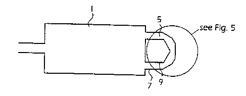
L'invention concerne un dispositif permettant de réfléchir des ondes lumineuses, servant à la construction de systèmes optiques destinées à différentes applications et de dispositifs spéciaux. Ce dispositif, réalisé sur un substrat et doté d'une structure plane, comprend un coupleur d'énergie lumineuse (1) de type interférentiel multimode (MMI), constitué d'une plaque rectangulaire située sur la surface du substrat ou à l'intérieur. Le coupleur partage la lumière incidente sur un terminal d'entrée en deux parties égales, chacune desquelles est acheminée vers un terminal de sortie. Le coupleur associe aussi la lumière arrivant sur les deux terminaux de sortie et l'achemine vers le terminal d'entrée. Une boucle, reliée aux deux terminaux de sortie, permet de transporter la lumière arrivant sur l'un des deux terminaux de sortie vers l'autre. Cette boucle est un guide d'onde plan, réalisé sur le substrat et relié à la surface d'un bord du coupleur. La boucle présente un contour extérieur (7) comportant plusieurs segments linéaires, et elle peut également présenter un contour intérieur (9), de forme polygonale. La forme de la boucle peut être obtenue en pliant à au moins deux reprises une bande d'épaisseur constante, les plis étant réalisés de manière symétrique.


Abrégé anglais


A device for reflecting light waves to be used when building optical systems
for various applications and special devices, is built on a substrate and has
a planar structure. It comprises a light power coupler (1) of the MMI-type,
configured as a rectangular plate at or in the surface of the substrate. The
coupler splits light incoming on an input terminal into two equal portions,
each portion delivered on an output terminal. Also the coupler combines light
incoming on two output terminals into combined light delivered on the input
terminal. A loop is connected to the two output terminals for conducting light
delivered on each one of these output terminals back into the other one of
these output terminals. The loop is a planar waveguide built on the substrate,
connected to an edge surface of the coupler. The loop has an outer contour (7)
comprising a multitude of linear segments and it can also have an inner
contour (9) having a polygon shape. The shape of the loop can be formed by
folding a strip having a uniform width at least twice, the folds being
symmetrically made.

Revendications

Note : Les revendications sont présentées dans la langue officielle dans laquelle elles ont été soumises.


6
CLAIMS
1. A device for reflecting light waves propagating in an optical waveguide,
the device
comprising a light power coupler having an input terminal and at least two
output terminals,
splitting light incoming on the input terminal into at least two shares of
light, each share
delivered on one of the at least two output terminals and combining light
incoming on the at
least two output terminals into combined light delivered on the input
terminal, the device
further comprising a loop connected to two of the output terminals, conducting
light delivered
on each one of these output terminals back into the other one of these output
terminals, char-
acterized in that the device is a planar device built on a substrate, the
coupler being a
substantially rectangular plate at or in the surface of the substrate and
having a refractive
index adapted to the refractive index of surrounding material and an adapted
size so that at an
input terminal is formed at a side of the rectangular plate and at least two
output terminals are
formed at an opposite side and the loop being formed by a planar waveguide at
the surface of
the substrate having an adapted refractive index and having an end segment at
one of the
output terminals and an end segment at another one of the output terminals.
2. A device according to claim 1, characterized in that the coupler is an MMI
coupler.
3. A device according to any of claims 1 - 2, characterized in that the loop
is a strip
having smooth curved outlines, a major portion of the loop being formed as
part of a circle.
4. A device according to any of claims 1 - 2, characterized in that the loop
is a strip
having polygon outlines comprising only straight line segments located in
angles to each
other.
5. A device according to any of claims 1 - 2, characterized in that the loop
has a
convex polygon outline comprising only straight line segments located in
angles to each other,
one of the straight line segments being a large side directly connected to
that side of the
rectangular plate forming the coupler at which the output terminals are
formed, the convex
polygon being symmetric in relation to a center line of the rectangular plate.
6. A device according to claim 5, characterized in that the rectangular plate
forming
the coupler and the planar waveguide forming the loop are integrated into one
unit plate
having a uniform refractive index.
7. A device according to claim 6, characterized in that the unit plate has an
outline
corresponding to a rectangle having an isosceles triangle at one of its sides.
8. A device according to claim 6, characterized in that the unit plate has an
outline
corresponding to a rectangle having a trapezoid at one of its sides.
9. A device for reflecting light waves propagating in an optical waveguide,
the device
comprising a light power coupler having an input terminal and at least two
output terminals,
splitting light incoming on the input terminal into at least two shares of
light, each share
delivered on one of the at least two output terminals and combining light
incoming on the at
least two output terminals into combined light delivered on the input
terminal, the device
further comprising a loop connected to two of the output terminals, conducting
light delivered

7
on each one of these output terminals back into the other one of these output
terminals, char-
acterized in that the loop is a planar waveguide at or in the surface of
substrate having a
refractive index adapted to the refractive index of material surrounding the
planar waveguide
and that the loop has the shape of a strip extending from one of the output
terminals to
another one of the output terminals.
10. A device according to claim 9, characterized in that the strip has smooth
curved
outlines, a major portion of the strip being formed as part of a circle.
11. A device according to claim 9, characterized in that the strip has polygon
outlines
comprising only straight line segments located in angles to each other.
12. A device according to any of claims 9 and 11, characterized in that the
strip has
outlines corresponding to the outlines of a strip which has a uniform width
and is folded at
least twice.

Description

Note : Les descriptions sont présentées dans la langue officielle dans laquelle elles ont été soumises.


CA 02356876 2001-06-22
WO 00/39616 PCT/SE99/02452
1
A DEVICE FOR REFLECTING LIGHT
TECHNICAL FIELD
The present invention relates to a device for reflecting light also called an
optical
reflection plug.
s BACKGROUND OF THE INVENTION
When building optical systems for various applications and special devices,
there may
be a need for providing a total reflection of Light. At present there is no
good established
method to produce a total reflection of light independently of the wavelength
of the light.
Metallizing the end of the waveguide by aluminum has been mentioned as a
possible way, see
,o M.V. Bazylenko, M. Gross, E. Gauja, and P.L. Cchu, "Fabrication of Light-
Turning
Mirrors in Buried-Channel Silica Waveguides for Monolithic and Hybrid
Integration", J.
Lightwave Technol. Vol. 15(1), pp. 148 - 153, 1997. When making optical
integrated circuits
having integrated waveguides metallization of vertical end surfaces is a
costly and
complicated process. Also the lifetime can be questioned. A method of
producing total
~s reflection for a relatively narrow wavelength range is to use Bragg
gratings. Using special
designs such as varying the grating period in the propagation direction a
total reflection over
a wider range could possibly be achieved. However, it is relatively costly to
produce Bragg
gratings and the production thereof requires costly equipment as well as a
large area on the
chip in the case where the totally reflecting structure is to be incorporated
in an integrated
zo circuit structure.
In L.V. Iogansen et al., "Multimode fiber interferometers", Optics and
Spectroscopy,
Vol. 58, No. 5, May 1985 optical reflectors using resonant tunnel loop
reflection are
disclosed. Simple loop reflectors are shown in fig. 5 in this document. There
are some losses
in such a loop reflector comprising loss in the waveguide, loss in the tunnel-
coupling section,
z5 and loss of radiation in the loop.
In the Japanese patent application JP 8-274398 a semiconductor laser module is
dis-
closed. It has a Loop mirror comprising a four-terminal fiber coupler and a
fiber loop
connected to the coupler.
SUMMARY OF THE INVENTION
3o It is an object of the invention to provide a device for reflecting light
waves to be easily
incorporated in integrated optical circuits.
A device for reflecting light waves is built on a substrate and has a planar
structure. It
comprises a light power coupler operating as a power sputter, preferably of
the MMI-type,
and conf gured as a rectangular plate at or in the surface of the substrate.
The coupler splits
35 light incoming on an input terminal into at least two equal portions, each
portion delivered on
an output terminal. Also the coupler combines light incoming on at least two
output terminals
into combined light delivered on the input terminal. A loop is connected to
two output
terminals for conducting light delivered on each one of these output terminals
back into the
other one of these output terminals. The loop is a planar waveguide built on
the substrate,

CA 02356876 2001-06-22
WO 00/39616 PCT/SE99/02452
2
connected to an edge surface of the coupler. The loop has preferably an outer
contour
comprising a multitude of linear segments and it can also have an inner
contour comprising a
multitude of linear segments. The shape of the loop can e.g. be formed by
folding a strip
having a uniform width at least twice, the folds being symmetrically made.
BRIEF DESCRIPTION OF THE DRAWINGS
The invention will now be described in detail by way of non-limiting
embodiments with
reference to the accompanying drawings, in which:
Fig. 1 is a schematic view from above illustrating the principle of a loop
minor
structure,
,o Fig. 2 is a view from above of a loop minor made as a planar structure on a
substrate,
Fig. 3 is a view from above of an alternative embodiment of a loop mirror made
as a
planar structure,
Fig. 4a is an enlarged view of the loop waveguide of Fig. 2 illustrating the
reflection
conditions,
,5 Fig. 4b is a sectional partial view of the loop waveguide as seen in the
direction of the
arrow A of Fig. 4a illustrating an embodiment of construction of the loop, in
particular at the
reflecting surfaces,
Fig. S an enlarged view of the loop waveguide of Fig. 3 illustrating the
reflection
conditions,
zo Fig. 6 is a view from above of a loop mirror having a loop integrated in a
coupler, and
Fig. 7 is a view from above of an alternative embodiment of a loop minor
having a
loop integrated in a coupler.
DESCRIPTION OF PREFERRED EMBODIMENTS
In Fig. 1 the basic construction of a loop minor is illustrated..A loop minor
comprises
i5 a 1x2 optical coupler 1, in the preferred case a 1x2 MMI (Mufti Mode
Interference)
waveguide coupler. The coupler operating as an equal power splitter having one
input
terminal and two output terminals. The two output terminals connected to each
other through
a light waveguide loop 3. MMI devices are described in e.g. L.B. Soldano and
E.C.M.
Pennings, "Optical Mufti-Mode Interference Devices Based on Self Imaging:
Principles and
3o Application", J. Lightwave Technol. Vol. 13(4), pp. 615 - 627, 1995, and
the published In-
ternational patent application W097/35220. The waveguide 3 may as conventional
be an
optical fiber but in the embodiment considered herein it is made as a planar
structure to be
used e.g. in PLCs (Planar Lightwave Circuits).
The waveguide 3 is then made as a strip of a first material embedded in a
layer of a
as second material having a different refractive index, the layer and strip
being produced at or in
the surface of a substrate, basically like electronic integrated circuits. The
second material
can be air and then the strip can be produced by etching a layer applied to
the surface of the
substrate. Typically however, the waveguide is made as a rectangular waveguide
comprising a
core having a rectangular cross-section made by etching a layer having a
suitable refractive

CA 02356876 2001-06-22
WO 00/39616 PCT/SE99/02452
3
index and further comprising .an undercladding layer and an overcladding
layer, these
different layers being formed of e.g. doped silicon oxide material or polymer
layers.
The waveguides used, both for conducting light at the input side of the
coupler 1 and in
the reflecting loop are preferably always designed to be single-mode or
monomode type.
s The loop 3 as illustrated in Fig. 1 is configured as a curved strip having a
smooth path
joining the terminal portions at the outputs of the coupler, these terminal
portions being
parallel to each other. The curved smooth portion of the loop has over a
substantial part
thereof the shape of part of a circle and thus has there a constant curvature.
The maximum
curvature must always be smaller than a value set by the difference of the
refractive index of
~o the waveguide and that of the surrounding material, since larger curvatures
and thus a smaller
radius of the loop would give unacceptable losses. For a small radius a too
large portion of
the energy of light propagating in the reflecting loop would leak out of the
loop.
Furthermore, if the difference of the refractive index n of the waveguide and
that (no) of the
surrounding material is large the loop will have a reasonably small diameter.
For instance,
~ 5 for a relative refractive index difference of 1.5 % , the diameter can be
smaller than 4 mm.
For smaller refractive index differences the circular loop structure will have
a larger diameter
and can in some cases take a too large space on a substrate.
Instead the waveguide of the loop can be made to have substantially a polygon
shape, as
is illustrated by the embodiments illustrated in the plan views of Figs. 2 and
3. The polygon
20 loop 5 is also here single-mode and comprises a curved strip-shaped region
having parallel
and identically shaped connection regions connected to the two outputs of the
coupler 1. The
waveguide 5 is limited by an exterior contour line 7 and an inner contour line
9, each being a
non-closed polygon Line comprising a plurality of straight linear segments.
The start and end
line segments of each polygon line 7, 9 are thus parallel to each other and
extend from the
is output side of the coupler 1 at right angles thereto. The two contour lines
7, 9 are, like the
loop of Fig. 1, symmetrical about a symmetry line extending from the center of
the line
connecting the outputs of the coupler l, i.e. about the longitudinal axis of
the coupler in the
case where it is an MMI-device.
In the loop waveguide structure 5 of Fig. 2 the exterior contour line 7 of the
waveguide
ao comprises straight linear pieces having directions deviating from each
other by 45 ° and thus
forming angles of 135° to each other, at the four corners of the
totally three straight line
segments required to connect the parallel start and end segments. The inner
contour line 9 has
only a total of three linear segments, one segment connecting the start and
end segments at
angles of 90°. The comers of the inner contour line are symmetrically
located in relation to
35 two corresponding corners of the exterior contour line 7, these two corners
connecting the
line segments connected directly to the start and end segments. The
propagation of light in
such a waveguide is illustrated in Fig. 4a. It appears from Fig. 4a, that for
the wavelength of
the used light, the material of the waveguide 3 should have such a refractive
index n in
relation to the refractive index no the surrounding material, e.g. air, that
the light propagating

CA 02356876 2001-06-22
WO 00/39616 PCT/SE99/02452
4
in the waveguide will be totally reflected for all incident angles r~ larger
than about 45 °, i. e.
practically for all incident angles which are larger than an angle somewhat
smaller than 45°,
see A. Stano, L. Faustini, C. Coriasso, D. Campi, C. Cacciatore, "OPTIMIZED
WAVEGIJIDE-INTEGRATED MIRRpRS", Proc. ECIO '97 EWF3, Stockholm, 1997, for a
detailed discussion.
In Figs. 4a and 4b also a construction of the loop waveguide 5 comprising
layers on a
substrate, not shown, is illustrated. The waveguide is constructed of an
undercladding 11, a
core or waveguide layer 13 and an overcladding 15. The layers forming the
undercladding,
the waveguide core and the overcladding are etched to have the required shape.
At the
,o reflecting surfaces 17 of the loop etched rectangular recesses or vents 19
are provided which
have accurately flat surfaces at the waveguide, these flat surfaces also being
accurately
perpendicular to the large surfaces of the structure.
If the total reflection condition cannot be fulfilled in the waveguide Layout
of Figs. 2
and 4a, a structure requiring a total reflection only for all incident angles
r~ larger than
,s somewhat more than 30° can be used, as is illustrated by the
embodiment of Fig. 3. Here the
exterior contour line 7 comprises seven linear segments located in angles of
I50° to each
other what corresponds to the condition that a linear segment of the contour
has a direction
deviating by an angle of 30° from those of the line segments connected
to the considered
linear segment. The interior contour line 9 comprises five Linear segments
having directions
zo deviating from each other by 60° or located in angles of 120°
to each other. The corners of
the interior contour line 9 are also here located symmetrically in relation to
segments of the
exterior contour line, on the line passing such a segment centrally at right
angles. The
propagation of light in this loop structure is illustrated in Fig. 5. The -
waveguide can be made
to include reflective surfaces to air like the embodiment of Fig. 4a by
providing recesses 19
zs from the surface of the structure. '
The contour lines of the structures of Figs. 2 and 3 can be obtained by
folding a strip of
material having a uniform width two and three times respectively. This can
easily be
generalized to folding more times, say n times. Then the resulting structure
will comprise an
outer contour line of 2n+ I line segments and an interior contour having n+ I
line segments.
3o The segments of the exterior contour have directions deviating from those
of the adjacent
segments by angles of 90°/n and the segments of the interior contour
have directions
deviating by angles of 2~90/n. The used light must be totally reflected at the
border surface
between the material of the waveguide and the surrounding material at all
incident angles
about 90°/n or larger than somewhat more than 90°/n.
35 A simplified reflecting structure can also be incorporated directly in a
MMI-coupler, see
Figs. 6 and 7. The MMI-coupler 21 is a planar structure and comprises a thin
layer of a
material having a refractive index adapted to be higher than that of the
surrounding material.
The layer has for a simple coupler a rectangular shape and forms the main part
.23 of the
reflecting structure. The rectangular body 23 is adapted so that for light
incoming into the

CA 02356876 2001-06-22
WO 00/3616 PCT/SE99/02452
layer centrally at a short side, two images of the incoming Iight wave will
appear at the
opposite short side at places symmetrically located in relation to the
longitudinal direction of
the rectangular shape. In Figs. 6 and 7 these pictures appear at the line 25.
In order to make such a simple reflecting structure the rectangular shape 23
is
5 supplemented with a polygon shape 27 at said opposite short side. The
polygon has a free
polygon line 29, which is symmetrical in relation to the longitudinal
direction of the
rectangular body 23. The polygon shape is in Fig. 6 an isosceles triangle
having a 90°-angle
at the free comer. In the embodiment of Fig. 7 it is a symmetric trapezium
having its oblique
sides located in directions deviating from the direction of the long sides of
the rectangular
,o body 23 by angles of 30°, i.e. from the longitudinal direction. For
suitable refractive index
conditions, as outlined above, light from the two images at the line 25 will
be reflected by the
oblique sides of the outer polygon shape 29, as is illustrated in Figs. 6 and
7.

Dessin représentatif
Une figure unique qui représente un dessin illustrant l'invention.
États administratifs

2024-08-01 : Dans le cadre de la transition vers les Brevets de nouvelle génération (BNG), la base de données sur les brevets canadiens (BDBC) contient désormais un Historique d'événement plus détaillé, qui reproduit le Journal des événements de notre nouvelle solution interne.

Veuillez noter que les événements débutant par « Inactive : » se réfèrent à des événements qui ne sont plus utilisés dans notre nouvelle solution interne.

Pour une meilleure compréhension de l'état de la demande ou brevet qui figure sur cette page, la rubrique Mise en garde , et les descriptions de Brevet , Historique d'événement , Taxes périodiques et Historique des paiements devraient être consultées.

Historique d'événement

Description Date
Inactive : Morte - Taxe finale impayée 2011-04-18
Demande non rétablie avant l'échéance 2011-04-18
Réputée abandonnée - omission de répondre à un avis sur les taxes pour le maintien en état 2010-12-21
Réputée abandonnée - les conditions pour l'octroi - jugée non conforme 2010-04-16
Un avis d'acceptation est envoyé 2009-10-16
Lettre envoyée 2009-10-16
Un avis d'acceptation est envoyé 2009-10-16
Inactive : CIB enlevée 2009-10-06
Inactive : Approuvée aux fins d'acceptation (AFA) 2009-01-19
Modification reçue - modification volontaire 2008-11-27
Lettre envoyée 2008-11-26
Modification reçue - modification volontaire 2008-11-18
Exigences de rétablissement - réputé conforme pour tous les motifs d'abandon 2008-11-18
Requête en rétablissement reçue 2008-11-18
Inactive : Abandon. - Aucune rép dem par.30(2) Règles 2007-12-07
Inactive : Dem. de l'examinateur par.30(2) Règles 2007-06-07
Modification reçue - modification volontaire 2007-05-07
Inactive : Dem. de l'examinateur par.30(2) Règles 2006-11-07
Inactive : CIB de MCD 2006-03-12
Lettre envoyée 2004-12-10
Toutes les exigences pour l'examen - jugée conforme 2004-11-29
Exigences pour une requête d'examen - jugée conforme 2004-11-29
Requête d'examen reçue 2004-11-29
Exigences relatives à la nomination d'un agent - jugée conforme 2003-11-19
Inactive : Lettre officielle 2003-11-19
Exigences relatives à la révocation de la nomination d'un agent - jugée conforme 2003-11-19
Inactive : Lettre officielle 2003-11-14
Lettre envoyée 2002-06-13
Inactive : Transfert individuel 2002-04-23
Inactive : Page couverture publiée 2001-10-26
Inactive : CIB en 1re position 2001-10-04
Inactive : Lettre de courtoisie - Preuve 2001-09-25
Inactive : Notice - Entrée phase nat. - Pas de RE 2001-09-21
Demande reçue - PCT 2001-09-20
Demande publiée (accessible au public) 2000-07-06

Historique d'abandonnement

Date d'abandonnement Raison Date de rétablissement
2010-12-21
2010-04-16
2008-11-18

Taxes périodiques

Le dernier paiement a été reçu le 2009-11-23

Avis : Si le paiement en totalité n'a pas été reçu au plus tard à la date indiquée, une taxe supplémentaire peut être imposée, soit une des taxes suivantes :

  • taxe de rétablissement ;
  • taxe pour paiement en souffrance ; ou
  • taxe additionnelle pour le renversement d'une péremption réputée.

Les taxes sur les brevets sont ajustées au 1er janvier de chaque année. Les montants ci-dessus sont les montants actuels s'ils sont reçus au plus tard le 31 décembre de l'année en cours.
Veuillez vous référer à la page web des taxes sur les brevets de l'OPIC pour voir tous les montants actuels des taxes.

Historique des taxes

Type de taxes Anniversaire Échéance Date payée
Taxe nationale de base - générale 2001-06-22
TM (demande, 2e anniv.) - générale 02 2001-12-21 2001-06-22
Enregistrement d'un document 2002-04-23
TM (demande, 3e anniv.) - générale 03 2002-12-23 2002-12-11
TM (demande, 4e anniv.) - générale 04 2003-12-22 2003-12-02
TM (demande, 5e anniv.) - générale 05 2004-12-21 2004-11-22
Requête d'examen - générale 2004-11-29
TM (demande, 6e anniv.) - générale 06 2005-12-21 2005-11-30
TM (demande, 7e anniv.) - générale 07 2006-12-21 2006-11-22
TM (demande, 8e anniv.) - générale 08 2007-12-21 2007-11-23
TM (demande, 9e anniv.) - générale 09 2008-12-22 2008-11-18
Rétablissement 2008-11-18
TM (demande, 10e anniv.) - générale 10 2009-12-21 2009-11-23
Titulaires au dossier

Les titulaires actuels et antérieures au dossier sont affichés en ordre alphabétique.

Titulaires actuels au dossier
TELEFONAKTIEBOLAGET LM ERICSSON
Titulaires antérieures au dossier
TORSTEN AUGUSTSSON
Les propriétaires antérieurs qui ne figurent pas dans la liste des « Propriétaires au dossier » apparaîtront dans d'autres documents au dossier.
Documents

Pour visionner les fichiers sélectionnés, entrer le code reCAPTCHA :


Pour visualiser une image, cliquer sur un lien dans la colonne description du document. Pour télécharger l'image (les images), cliquer l'une ou plusieurs cases à cocher dans la première colonne et ensuite cliquer sur le bouton "Télécharger sélection en format PDF (archive Zip)" ou le bouton "Télécharger sélection (en un fichier PDF fusionné)".

Liste des documents de brevet publiés et non publiés sur la BDBC .

Si vous avez des difficultés à accéder au contenu, veuillez communiquer avec le Centre de services à la clientèle au 1-866-997-1936, ou envoyer un courriel au Centre de service à la clientèle de l'OPIC.


Description du
Document 
Date
(aaaa-mm-jj) 
Nombre de pages   Taille de l'image (Ko) 
Dessin représentatif 2001-10-22 1 3
Abrégé 2001-06-21 1 56
Description 2001-06-21 5 322
Dessins 2001-06-21 3 39
Revendications 2001-06-21 2 98
Revendications 2007-05-06 2 72
Description 2008-11-17 7 342
Revendications 2008-11-17 2 84
Description 2008-11-26 7 354
Revendications 2008-11-26 2 90
Avis d'entree dans la phase nationale 2001-09-20 1 210
Courtoisie - Certificat d'enregistrement (document(s) connexe(s)) 2002-06-12 1 114
Rappel - requête d'examen 2004-08-23 1 117
Accusé de réception de la requête d'examen 2004-12-09 1 177
Courtoisie - Lettre d'abandon (R30(2)) 2008-03-02 1 168
Avis de retablissement 2008-11-25 1 170
Avis du commissaire - Demande jugée acceptable 2009-10-15 1 162
Courtoisie - Lettre d'abandon (AA) 2010-07-11 1 164
Courtoisie - Lettre d'abandon (taxe de maintien en état) 2011-02-14 1 173
Correspondance 2001-09-20 1 24
PCT 2001-06-21 8 356
Correspondance 2003-10-30 8 382
Correspondance 2003-11-13 1 13
Correspondance 2003-11-18 1 26