Note : Les descriptions sont présentées dans la langue officielle dans laquelle elles ont été soumises.
CA 02358018 2001-10-02
-I-
This invention was made with Government support under contract number DE-
AC02-98CH10886, awarded by the U.S. Department of Energy. The Government has
certain rights in the invention.
FIELD OF THE INVENTION
The present invention is directed to an apparatus and method for a wide
tracking
range phase lock loop ("PLL") with exceptionally low fitter. In particular.
the present
invention relates to PLL applications that require low phase noise or zero
crossing fitter
for encoded transmissions. A PLL of the present invention separates the clock
from the
encoded data such that the recovered clock and data are both reduced
signiticantlv in
fitter. This is ven~ helpful in accurate position control applications that
require precise
phase. spatial or time measurement or control.
BACKGROUND OF THE INVENTION
It is often necessary in communication. digital audio and similar applications
to
lock to an external clock or reference while generating a new clock source
that is immune
to various sources of phase and frequency noise in the incoming reference
signal. In order
for a receiver to receive and capture data, as referenced to a transmitter's
clock signal, it
is necessary for the receiver to have a clock signal that is synchronized or
phase aligned
to the same clock signal.
CA 02358018 2001-10-02
-2-
Phase locked loop (PLL) circuits have been commonly used for the purpose of
generating a signal in a preferred phase relationship relative to another
signal. A PLL
carefully adjusts to its ow clock (the "local oscillator') to bring it into
precise alignment
with some external signal (the "reference clock"). In serial data
communications and
similar applications. the reference clock is often embedded in a stream of
data bits. It is
the PLL's task in a clock recovery subsystem to align its local oscillator
with the
reference clock information embedded in the data stream. The PLL circuit
within the
receiver can adjust its local clock signal frequency to a multiple of the
reference signal
frequency, thereby phase aligning the two signals together. The phase
relationship
between the reference signal and the local clock signal is then referred to as
being locked.
Once properly aligned. the local oscillator can be used to clock bits out of
the data stream,
sampling each data baud right in the center at the point of maximum noise
immunity.
As illustrated in Figure I, a conventional PLL 10 provides a feedback system
combining a voltage-controlled oscillator (VCO) 12 and a phase comparator or
detector
14 in electronic communication therewith such that the oscillator frequenc~~
or phase
accurately tracks that of an applied frequency or phase-modulated signal.
respectively. In
a PLL. the error signal from the phase comparator is the difference between
the ~nput
frequency or phase and that of the signal fed back. If f,~ does not equal
f"~~, phase
comparator 14 generates a phase error output signal that is a measure of the
phase
difference. The phase error signal, after being filtered by loop filter 16 and
amplified by
amplifier 18, causes f"co to deviate in the direction of f.,4. The VCO will
eventually
''lock'' to f,~ so as to maintain a fixed relationship with the input signal.
CA 02358018 2001-10-02
-3-
In this application. any imperfections in a transmit clock that is used to
construct a
data stream may compromise the ability of the PLL to properly align its local
oscillator.
Imperfections in the transmit clock are sometimes classified as frequency
offsets. wander
or, as used herein, ''fitter". fitter, a common problem associated with PLL
circuits, can be
defined as abrupt. spurious variations in the phase of successive pulses as
referenced to
the phase of a continuous oscillator, causing deleterious variations in the
output
frequency. As the fitter frequency on the input signal increases, the
bandwidth
requirements of the PLL likewise increase. The precision of the recovered
clock,
therefore, is a limitation on system performance.
With the introduction of more sophisticated services involving the transfer of
large amounts of information such as digital data, video or voice data,
communication
networks must provide predictably superior levels of performance while
ensuring the
maintenance of data quality. In a digital communication system. for instance.
one
application of a PLL may be to provide a ''clean" clock signal which has the
same
frequency and phase as a received digital data signal that is to be decoded. A
typical
digital PLL design uses a reference clock having a frequency that is much
higher than
that of an incoming data signal to generate the output clock. This approach.
however, can
only guarantee a phase lock that is within one clock period of the reference
clock. This
error in the phase lock constitutes fitter. In analog conventional PLL
circuits fitter is
commonly caused by the errors in the filtering of the control voltage and VCO
noise.
Once fitter contaminates a signal, it propagates through a system, often
increasing
as it passes through various devices. PLLs have therefore traditionally found
limited use
CA 02358018 2001-10-02
in those systems requiring very high stability. Systems incorporating radar
oscillators. for
example. require very high stability that can only be provided by narrowin~_=
the loop
bandwidth. This in tum degrades the frequency tracking performance of the PLL
and
detracts from an inherently desirable feature of PLL oscillators. When the
loop gain of
the PLL is high. the pull-in and lock-in times are short, yet the sensitivity
to noise (both
internal and external) becomes high, resulting in large phase fitter and
frequency fitter in
the output. On the other hand, when the loop gain of the PLL is low and the
bandwidth is
narrow so as to remove noise, the pull-in and lock-in capabilities for the
frequency offset
and the initial phase difference become low, resulting in narrower pull-in and
lock-in
ranges. The narrow bandwidth of the loop not only takes a long time to achieve
the lock-
in state for a large frequency offset but also presents difficulty in holding
the lock-in state
for a frequency shift. It therefore becomes difficult for the loop to lock,
and track and
carrier loss is realized.
It is therefore desirable to construct a low fitter PLL that has a relatiwlv
large
bandwidth by controlling harmonics that creep in at higher bandwidths. Good
harmonic
suppression is important in PLLs because this affects loop characteristics (
i.e.. stability,
phase error, jittery. Although not readily apparent. harmonics with balanced
codes exist
off of the fundamental that can cause false locks with pseudo-random code
streams. A
PLL that exhibits optimum harmonic suppression is therefore not only
beneficial in
reducing fitter on the transmit side, but it is also instrumental in rejecting
noise and
transmission-media-induced distortions on both of the reception and
instrumentation
sides.
CA 02358018 2001-10-02
-S-
SUMMARY OF THE INVENTION
The present invention provides a wide tracking range phase locked loop (PLL)
circuit that achieves minimal fitter in a recovered clock signal. The PLL of
the present
invention is particularly adapted for applications that require excellent
stability (i.e., low
phase noise and/or low phase drift). The PLL of the present invention is
further
applicable for encoded transmissions containing clock and/or data such that
the recovery
of such clock and/or data is effected without the need for signal acquisition
preambles,
while avoiding harmonic locks in fixed and/or swept frequency systems.
The PLL circuitry disclosed herein provides a means to produce a low fitter
recovered clock regardless of the source of the fitter (i.e. whether it is in
the source or the
transmission media) and has automatic harmonic lockout detection circuitn~
through
means of a novel lock and seek control logic in electrical communication with
a
programmable frequency discriminator and a code balance detector. The
frequency
discriminator enables preset of a frequency window of upper and lower
frequency limits
to derive a programmable range within which signal acquisition is effected.
The
discriminator works in combination with the code balance detector circuit to
minimize
the potential for false lock. Useable frequency sweeps may thereby extend
through
several frequency harmonics while avoiding such harmonics during signal
acquisition.
This allows a large frequency swept range without a preamble to be used while
avoiding
harmonic lockup during acquisition.
In addition, the combination of a differential loop integrator with the lock
and
seek control logic guarantees swift signal acquisition with a clean noise
output signal
CA 02358018 2001-10-02
-6-
without harmonic lockup. This combination allows a larger dynamic range by
programmable means as compared to other design topologies, thereby allowin~~
greater
flexibility. and large swept frequency ranges.
An adaptive cable equalizer is desirably used in combination with the present
invention PLL to recover encoded transmissions containing a clock and/or data.
The
adaptive cable equalizer is a low-cost monolithic solution for equalizing data
transmitted
over cable or any other media having similar dispersive loss characteristics.
The
equalizer automatically adapts to equalize short haul cable lengths of coaxial
and twisted
pair cables or wires and provides superior fitter performance itself. The
combination of
the equalizer with the present invention PLL is desirable in that such
combination permits
the use of short haul wires with the added advantage of significantly reduced
source fitter.
Using the PLL circuit of the present invention, no signal acquisition
preambles
are required to avoid harmonic locks in fixed, intermittent and/or swept
frequency
systems. This PLL will automatically seek and lock onto fixed and/or varying
frequency encoded input signals and reject harmonics of the encoded signal
stream.
The disclosed technique further permits large frequency sweeps through
harmonics
without the potential for harmonic lockup on signal acquisition. Ligitai input
data is re-
clocked by a low fitter recovery clock and demodulated. The output-recovered
clock
desirably has a 50% duty factor. The described technique will work for any DC
balanced code modulation scheme used in most high capacity digital
transmission and
storage devices.
It is important that the implementation of the present invention PLL generates
CA 02358018 2001-10-02
_7_
the least possible switching noise. It is further important that optimum
analog and
digital noise isolation and shielding are achieved through precise PWB design
using
isolated solid power planes for both analog and digital circuitry.
It is therefore an advantage of the present invention to provide a PLL that is
highly immune to input signal fitter.
It is another advantage of the present invention to provide a PLL that
recovers
the accuracy of the original clock in a noise transmission environment with
the least
possible fitter.
It is an additional advantage of the present invention to provide such a low
fitter
PLL that achieves wide range tracking with low phase error and drift for data
and clock
recovery.
It is yet another additional advantage of the present invention to provide a
tow
fitter PLL in a compact and inexpensive design that uses commercially
available
technology.
It is still another advantage of the present invention to implement a low
fitter
PLL for both fixed and swept frequency systems.
It a further advantage of the present invention to provide a PLL havin_ an
output
that maintains a constant phase relationship with its input, even over a large
range of
input frequencies. The PLL, having one reference clock input and multiple
buffered clock
outputs, continuously monitors the relation between the phase of the input
reference clock
and the phase of the outputs. The PLL then adjusts the output transitions so
that they
land precisely on top of the input transitions within a tight timing window.
CA 02358018 2001-10-02
_8_
BRIEF DESCRIPTION OF THE DRAWINGS
Figure 1 is a functional block diagram of a conventional phase lock loop
circuit.
Figure 2 is a functional block diagram of a low fitter phase lock loop circuit
of
the present invention.
Figure 3 is a circuit diagram of a desired embodiment of a frequency
discriminator used with a phase lock loop circuit of the present invention.
DETAILED DESCRIPTION OF THE PREFERRED EMBODIMENTS
The present invention provides for a phase lock loop (PLL) that recovers a
reference clock and reduces fitter from a serial data stream that is
transmitted thereto.
The low fitter PLL output clock is used to clock counters for accurate delays
and then
buffered for further distribution. Sub-nanosecond fitter is achieved with the
,
combination of an adaptive cable equalizer at the PLL input and the use of a
digital
frequency discriminator that avoids harmonic lock-up on signal acquisition.
Implementing a differential loop integrator further attenuates fitter. The
integrator that
is holding the last lock-on voltage then only has to slew over a narrow range
to track.
This limits the control voltage swing and hence the probability of crossing
over and
finding a nearby harmonic.
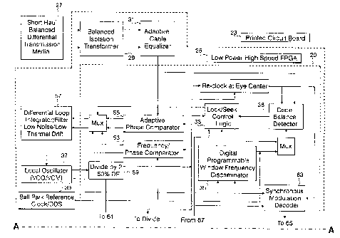
Now referring to the tigures, wherein like elements are identically numbered,
a
functional block diagram of a phase lock loop ("PLL") circuit 20 of the
present invention
is shown in Figure 2. PLL 20 and components in electrical communication
therewith
(further described hereinbelow) are supported by a printed circuit board (PCB)
23. T'he
CA 02358018 2001-10-02
-9-
architecture for PLL 20 is similarly sustained on a field programmable gate
array (FPGA)
25, that enables fast prototvping of circuits as is commonly known in the art.
At least one short haul transmission medium 27 furnishes a conduit for
transfer of
an incoming data stream from a transmitter source (not shown) to PLL 20.
Transmission
medium 27 is desirably selected from short haul cable lengths of coaxial and
misted pair
cables. wires and the like desirably having a maximum length of about 320'. A
balanced
isolation transformer ?9 is desirably coupled in electrical communication with
transmission medium ?7 for translating the incoming data stream onto PCB 23.
An adaptive cable equalizer 31 is provided that is coupled between balanced
isolation transformer ?9 and PLL 20 for reducing fitter inherent in the
incoming data
stream. Adaptive cable equalizer 31 allows short runs on inexpensive twisted
wire pairs
such as those found on fanouts to local devices. Adaptive cable equalizer 31
further
adjusts for the lowest incoming fitter independent of cable length as a signal
pre-
conditioner to PLL ?0. reducing system fitter thereby. Adaptive cable
equalizer 31 may
be selected from anv of a plurality of commercially available embodiments that
are well
known in the art.
PLL ?0 implements an "autoranging" technique that e.iabies preprogramming of a
discrete frequency 4vindow within which an incoming signal is identified to
which lock is
effected. Such autoranging capability is executed by a lock and seek control
logic 33.
Control logic 33 has a first input that is connected to an output of a digital
programmable
frequency discriminator 35 (further described hereinbelow) in electrical
communication
with a balance code detector circuit 36. Balance code detector fault is the
first indication
CA 02358018 2001-10-02
-10-
of a possible harmonic lockup but is not sufficient alone since the received
data may
contain errors. Frequency discriminator 3~ verifies re-acquisition to enable
precise
programming of a wide frequency tracking range; this sets the window frequency
frame
within which a signal shall be "locked" to derive data from the data stream
and further
provide harmonic lockup protection over the prescribed range. An exemplan~
model of a
frequency discriminator for use with the present invention is illustrated in
Figure 3 and
further described hereinbelow.
Frequency discriminator 35 uses dividers and frequency-phase comparators to
set
an upper and lower window around a local clock signal generated by a local
oscillator or
clock 37. Frequency discriminator ~ ~ produces an output voltage that depends
on an
instantaneous signal frequency generated in response to the local clock signal
and an
input reference signal ~~enerated by a reference clock 39. Its signal is also
utilized as a
feedback signal within the loop. Local oscillator 37 is shown in Figure 2 as a
VCO or
VCM that is well established in the art as an electronically tunable
oscillator in which the
output frequency is dependent on the value of an applied tuning voltage.
Improved fitter
performance can be easily attained by the use of low phase noise differential
signal
VCOs. It is understood. however, that the type of tunable oscillator
implemented with the
present invention may be modified without departing from the scope thereof.
Further referring to Figure 2, reference clock 39 provides a baseline
reference
frequency to frequency discriminator 35 and is selected from an external fixed
clock such
as a crystal reference clock or an external dynamic clock such as a direct
digitally
synthesized (DDS) clock. Reference clock 39 eliminates any analog tuning
components,
CA 02358018 2001-10-02
-11-
thereby eliminating the drift and aging characteristics associated with such
devices. A
DDS reference input may be used to quickly acquire and track a known
frequenev,'time
profile within a narrow window while avoiding harmonics with low signal to
noise ratio
(S/N) inputs. Reference clock 39 therefore provides a "ball park" clock
reference to
frequency discriminator 35 and a basis for creating an exact frequency window
using
programmable counters. This window will not drift or vary with age as occurs
with
conventional control voltage threshold detectors.
Frequency discriminator 35 further uses programmable counters that can make
the
frequency window as small as needed to ensure that no harmonics with
sufficient power
to cause lock with the selected filter network will occur. As further shown in
Figure 3, an
illustrative frequency discriminator 35' conducive to operation of the present
invention
PLL ?0 is provided wherein frequency discriminator 35' includes an upper
frequency
threshold counter 45 and a lower frequency threshold counter 47 for
establishing
threshold settings around the local clock signal. Each of upper counter 45 and
lower
counter 47 divides the reference clock signal by a distinct predetermined
divisor.
Frequency discriminator 35' further includes a reference clock frequency
counter =19 that
divides the local clock signal by a predetermined divisor to generate a local
reference
clock signal.
Frequency discriminator 35' includes at least one frequency phase comparator
51
having an input from one of lower frequency threshold counter 45 and upper
frequency
threshold counter 47, and an input from reference clock frequency counter 49.
Comparator 5 I establishes at least one of a minimum frequency and a maximum
CA 02358018 2001-10-02
-12-
frequency that will not cause reacquisition of the reference clock signal. In
practice it may
be necessary to inhibit the output of local oscillator 37 many times to
determine if the
window is narrow enough to avoid harmonics, however. the tracking range will
be hard
limited b~~ this window.
Referring back to Figure 2, a frequency/phase comparator ~3 is provided in
electrical communication with reference clock 39. Comparator ~3 detects the
phase
difference between the reference frequency input and the signal frequency
input from the
VCO. Frequency/phase comparator ~2 locks on to the input reference signal to
effect the
locking step.
An adaptive phase only comparator » is provided in electrical communication
with lock and seek control logic 33 w herein phase only comparator »
determines a phase
difference between the input reference signal and the local clock signal when
lock is
effected therebetween. Phase comparator 55 then generates a phase error signal
corresponding to this phase difference and in proportion to the period so as
to adapt to
changing input frequency and thereby reduce phase lead and/or lag over a wide
frequency
spectrum. Phase comparator >j minimizes phase drift by varying output pulse
width
proportionally with frequency to accommodate a wide dynamic and swept ti-
equency
range with low phase error. The integration of phase comparator » therefore
results in
equal fitter specifications over the entire control voltage, translating to a
full frequency
range over a large frequency span.
A differential Loop integrator or filter 57 is also provided in PLL 20 wherein
filter 57 not only reduces frequency-dependent phase shift error, but also
reduces
CA 02358018 2001-10-02
-13-
temperature induced phase drift. Differential loop filter 57 is in electrical
communication with each of adaptive phase comparator SS and frequency/phase
comparator 53. Differential loop filter 57 generates a voltage control signal
that
corresponds to the phase error signal generated by phase comparator SS and
delivers
such control voltage signal to local oscillator 37. Upon achievement of said
locking
step, PLL 20 transmits this control voltage into the programmable range of
frequency
discriminator 35 so as to repeatedly lock the circuit to the input reference
signal.
Differential loop filter 57 towers control voltage noise, increases
sensitivity and
dynamic range, increases frequency tracking range, increases common mode noise
rejection, compensates for component variations and reduces thermal drift and
fitter.
Filter 57 thereby adapts to component variations so as to minimize the effects
of
thermally induced phase shift and noise.
PLL 20 further includes a divider 59 (shown herein as a divide-by-? divider)
in
electrical communication with local oscillator 37 to provide a low fitter
recovered clock
61 having ~0% duty factor. PLL 20 additionally has a synchronous modulation
decoder
circuit 63 having inputs from local oscillator 39 and the data stream for
demodulating
re-clocked digital input data from the data stream and recovering the re-
clocked data 63
therefrom. Demodulation of a signal takes place at a receiver located some
distance from
the transmitter. The process whereby demodulation is carried out by a second
multiplication requires that the carrier available at the receiver be
precisely synchronous
with the carrier used in the modulation process. Synchronous modulation
decoder circuit
63 may be selected from a plurality of modulation methods that are known
within the art
CA 02358018 2001-10-02
-14-
(i.e.. this can be "IP'~ or other logic implemented in the FPGA. although any
type
conducive to operation of the present invention will suffice).
PLL 20 optionally includes a reference override 67 in electrical communication
with lock and seek control logic 33. Reference override 67 will force the lock
on the ball
park reference 39 when no input signal is available.
PLL 20 may also include at least one indicator (not shown) for indicating when
PLL 20 has not attained signal acquisition and lock. The indicator. which may
be an
LED indicator or the like, is desirably pulse-stretched so that intermittent
problems can
be readily visualized. The indicator can therefore illuminate when out of
lock.
At the initiation of signal transmission. then, there are two frequencies
applied to
phase comparator ~~. As the loop acquires lock, PLL 20 must deal with mvo
different
ranges: one in the area in which frequency lock is acquired and, only after
frequency lock
has been accomplished, one in which phase lock occurs. In operation,
frequencv/phase
comparator ~3 first establishes lock-in with reference clock 39. Once
frequenc~-,~phase
lock is established and the phase error is minimized as the control voltage
stabilizes.
phase comparator » switches in for phase encoded data separation. Phase
comparator W
determines the phase differences between the input signals and the local
reference. The
rising edge of local oscillator clock 37 is measured against the pseudo-random
code
generator crystal output as a trigger to make j fitter measurements. The
detected phase
error signal is filtered so as to reduce noise and is sent thereafter to local
oscillator 37.
Oscillator 37 adjusts the frequency of the locally generated signal
accordingly to
approach lock.
CA 02358018 2001-10-02
-15-
A "ball park'' frequency is selected by producing a digital clock frequency
that
will center the window established by frequency discriminator 35. Frequency
lock must
be established first. then phase lock. Frequency discriminator 35 will
therefore force
frequency comparator 53 to be used, and when this locks, phase comparator 55
can be
used. Thus. when stable lock is attained, lock and seek control logic 33
switches over to
adaptive phase comparator 55, a frequency compensated phase detector for swept
frequency systems. Since filter 57 will not allow a step response when
switching away
from reference clock 39 over to the input signal, the output of filter 57 is
initially within
the ball park VCO control voltage to achieve the desired frequency for any
given set of
initial conditions, even with component variations from unit to unit. PLL ?0
then, upon
frequency lock, confines the rather arbitrary control voltage now to the ball
park
frequency. Only a small adjustment to the control voltage now will lock the
output of
tiler 57 to the desired frequency every time. In this configuration,
frequency/phase
detector 53 determines initial point frequency so that no tuning is necessary
even with
component variations between filter 57 and local oscillator 37. In this
manner, hard limits
can be precisely set without deleterious effects from component aging or
variation as is
found with analog frequency comparators.
Lock and seek logic 33 will automatically attempt to re-acquire if no lock is
detected after a programmable frequency dependent input delay. Logic 33 will
then
return to locking on the reference frequency and the cycle repeats itself. If
the input
signal does not get kicked out by frequency discriminator 35, then an accurate
and
harmonic-free lock has been achieved. A pulse stretched indicator as described
CA 02358018 2001-10-02
-16-
hereinabove desirably indicates successful phase lock on the input signal.
Frequency discriminator 35. in combination with PLL 20. can restrict operation
to
a precise frequency range having its accuracy determined solely by the high
accuracy of
reference clock 39. This can be useful in deciphering frequency division
multiplexed
signals over transmission media without the need for preambles. Discriminator
3~ may
alternatively be used to hold or constrain the output frequency of local
oscillator 37 when
a signal is lost or interrupted. In fixed or periodic swept frequency systems,
a fixed
frequency reference may be used to quickly and accurately set the initial
local oscillator
control voltage for fast signal acquisition, and to establish a programmable
and precise
fixed frequency tracking window. A narrow window can be established for fixed
frequency or a wider window established for swept frequency inputs.
The control signals generated by phase comparator 55 are proportional to the
input signal period to keep phase offset minimized. Phase comparator 55
therefore
allows a very wide range of input frequencies as the period is divided in half
before the
control voltage outputs are produced. This reduces and nearly eliminates phase
shift
for swept frequency systems, such as those that are commonly found in high
velocity
systems (i.e., missile, aircraft and satellite systems, as well as pauicie
accelerators).
Precise timing applications for these systems require low fitter and precise
aperture
windowing.
An illustrative example of the operation of the present inventive PLL is
provided
in the example below. It is emphasized that the values provided herein merely
constitute
an example of the efficiency with which the present process can be completed.
and that
CA 02358018 2001-10-02
-17-
these values can be affected as described thoroughly hereinabove. It is
therefore
understood that any or all steps may be modified in sequence or duration to
adapt to
different applications
Example
Frequency discriminator window threshold settings:
*The upper frequency (UF) threshold counter is set to divide a recovered 2X
reference clock = 56 MHz by 52
*The lower frequency (LF) threshold counter is set to divide a recovered 2X
reference clock = 56 MHz by 60
*The crystal reference clock = 14.318 MHz is divided by 14.
56 MHz/52 - 1.08 MHZ (high threshold)
56 MHZ/60 - 0.938 MHz (low threshold)
14.318 MHz/ 14 = 1.023 MHz (reference).
When the reference is between the high and low thresholds
(0.938 MHz < = 1.023 MHz < = MHz < = 1.08 MHz),
the trequency discriminator will not attempt to reacquire the signal.
Using the above settings with a 14.318 reference crystal clock oscillator:
1. ) The minimum frequency that will not cause reacquisition is:
LF/52 = 1.023 MHz thus LF = 53.196 MHz (low threshold )
2.) The maximum frequency that will not cause re-acquisition is:
HF/60 = 1.023 thus HF = 61.38 MHz (high threshold)
The following stable harmonics have been identified using a 14.318 MHz
CA 02358018 2001-10-02
-18-
reference oscillator with a desired 57.272 MHz fundamental PLL frequency using
the
phase only comparator:
MHz Harmonic Ratio Decimal
32.7274 4/7 0.571428
~
34.3637 6/ 10 0.6
38.1819 2/3 0.666666
40.0910 7/10 0.7
40.9092 5i7 0.714285
42.9547 3/4 0.75
45.8183 8/10 0.8
47.7274 SI6 0.833333
Other integer ratio harmonics are possible, but these lacked sufficient power
to
cause a harmonic lock in the test set over the tracking range (28 MHz through
80
MHz). For example, the 7/9 harmonic did not occur. The frequency discriminator
prevents these harmonics.
Using the same ratios for the 2X reference clock at +0% , -0.3 % for an
approximately 56 MHz operation, the following possible harmonics were
predicted
using the same harmonic ratios as above.
CA 02358018 2001-10-02
-19-
-0.3% (MHz) 0% (MHz) Harmonic Ratio
32.07 32.17 4/7
33.68 33.78 6/10
37.42 37.53 2/3
39.29 39.41 7/10
40.09 40.21 5/7
42.10 42.23 3/4
44.90 45.04 8/10
46.78 46.92 5/6
The ~S % discriminator threshold at 53.196 MHz is well above the next nearest
stable harmonic (5/6).
Testing reveals lock-up without harmonic lock every time, illustrating the
s
predictability and repeatability of PLL 20 performance. Such predictable
operation is
important in guaranteeing that a plurality of PLLs will all achieve lock in
critical
systems, as there is no practical way to "bump" any PLL that does not gain
harmonic-
free lock-up on encoded data in a broadcast system. Each PLL unit must achieve
lock
the first time without any re-tries when signal cables are attached to a
running system
and without preambles. This allows clock and data to b: seaa c~_ = ,;-ngle
trans~.~ission
medium without compromising fitter performance. The advantages are large when
compared to dual media systems, as small thermal shifts will change the phase
of the
clock of the data, not only resulting in irretrievable data loss but also
requiring precise
media length matching and thermal compensation.
In addition, the temperature performance of PLL 20 is excellent due to the
CA 02358018 2001-10-02
-20-
implementation of differential filter 57 in combination therewith. Filter 57
resolves to
nanovolt control voltages for picosecond resolution and precision in phase.
This
frequency sweep range performance goes well beyond that of VCOs commonly used
to
recover data in high bit rate (i.e. fixed frequency) communications systems.
PLL 20
thereby separates clock from data such that the recovered clock and data are
reduced
significantly in fitter. This is very beneficial for accurate position control
systems.
In the present embodiment, PLL 20 has a desirable fitter of about 50 ps, a
maximum RMS fitter of 125 ps and a maximum peak-peak fitter of 1 ns when used
in
lengthy cable distribution systems with swept frequency inputs and phase
modulated
data. It can be used in numerous applications with data rates ranging from a
few Hz to
several GHz.. For simple clock multiplication applications, the fitter is
better than 25
ps RMS in the 10 to 50 MHz range. These ranges, however, are not hard limited
by
the scope of this disclosure and merely serve as an illustration of the fitter
attenuation
that is attainable by the inventive circuit topology.
The PLL of the present invention therefore exhibits differential locking
capability
over a larger range of frequencies than those attainable by conventional PLLs.
The
present invention PLL works on the data stream itself. exhibiting an
''autoranging~~
capability- wherein the PLL locks onto different frequencies without harmonic
lockup.
This technology could be used to advance transmission electron microscope
images,
MRI equipment, telescopes, electronic lenses, filters, any instrument that
accepts
wavelength information and it is desired to stabilize the image of that
wavelength under
CA 02358018 2001-10-02
-21-
varying input conditions. The result is a sharper image and more precise
positions for
fixed or moving point targets.
The PLL disclosed herein, especially in combination with an adaptive cable
equalizer, can solve many imaging, transmission and position measurement
problems
involving noise-limited precision due to transmission media property shifts.
Consequently, it is also possible to stabilize the image of rapidly moving
targets with
PLL 20. Implementation of the present invention is advantageous in a myriad of
applications, which includes but is not limited to those applications
requiring precise
space and time measurement (i.e., telemetry, trajectory, radar, Doppler radar,
phased
array radar and guidance systems; global positioning satellite equipment,
satellite
communications equipment, survey equipment, IiDTV and other precise
positioning or
measuring equipment). The present invention is also desirable for picosecond-
adjustable passive fiber optic delays; high baud rate receivers; range and
velocity
finding or trajectory measurement equipment; gyroscopes; precise high speed
rotation
measurement and control such as is used in scanners, printers, scanning image
surveillance satellites, or attitude correction electronics; communications
systems: and
systems with large inertial damping requirements. The above described
~ombinat«~n of
features consistently yields incrementally better results relative to
conventional PLL
circuits. Most PLL systems are designed to operate over a relatively narrow
frequency
range, and preambles are commonly used to prevent harmonic locks. The present
invention PLL is performance oriented and many of its enhancements are
performance
related with its large swept frequency range and large frequency span. The PLL
design
CA 02358018 2001-10-02
-22-
disclosed herein can therefore "seek" over encoded data harmonics without lock-
up on
those harmonics during signal acquisition. This design requires no preamble to
attain
its harmonic-free lock performance.
Swept systems require a large tracking range that may pass through several
harmonics of the source signal. This design provides all of the necessary
detection
circuitry to prevent any harmonic lockups upon signal acquisition with encoded
data
without any false locks due to power up or signal interruption. This design
has no analog
comparator that could drift with temperature and range
The signal information processing techniques achieved by the present invention
PLL can further produce a new level of clarity or certainty at many points in
space at
the same time if the distributed signal aperture is adequately stabilized in
time to
picoseconds or better. These techniques can pass data along with the signal
such that
many distributed devices can share the same broadcast information. With
loopback
techniques, the timing can be equalized over great distances through a noisy
transmission media that may experience variations due to temperature, Doppler
effect
or physically curved Trajectories. The resultant signal can be automatically
trimmed to
noise floor accuracy, in both resolution and precision.
Various changes to the foregoing described and shown methods and
corresponding structures would now be evident to those skilled in the art. The
matter set
forth in the foregoing description and accompanying figures is therefore
offered by way
of illustration only and not as a limitation. Accordingly, the particularly
disclosed scope
of the invention is set forth in the following claims.