Note : Les descriptions sont présentées dans la langue officielle dans laquelle elles ont été soumises.
CA 02358185 2001-07-06
WO 00/41344 1 PCT/US99/30616
POLARIZATION MODE DISPERSION COMPENSATION VIA AN
AUTOMATIC TRACKING OF A PRINCIPAL STATE OF POLARIZATION
Field of the Invention
The present invention relates to method and
apparatus for providing polarization mode dispersion
compensation in high-speed optical transmission networks
and systems.
Background of the Invention
Polarization mode dispersion (PNm) has become one of
the most important limiting factors for high-speed
optical communication systems, especially for existing
optical networks. The existing optical fiber networks
have poor PNm characteristics with the PNm ranging from
0.5 to 2 ps/km~, corresponding to transmission distances
of 400 km down to 25 km for 10 Gbit/s systems. As
optical networks evolve, it is highly desirable to
transport data over long distance. For example, long
distance transmission is crucial for four-fiber
bidirectional line switched rings (BLSRS) since the
protection path can be as long as the whole optical ring.
Therefore, PNd7 compensation has become an urgent issue
for high-speed optical communication systems. Although
new fiber networks have better P1~7 performance and can
support 10 Gbit/s transmission over reasonably long
distance, PNm will become a limiting factor for 40 Gbit/s
transmissions. As the capacity demands keep increasing,
it is desirable to increase the bit-rate from 10 Gbit/s
to 40 Gbit/s. Therefore, PNm compensation is very
important not only for existing optical fiber networks,
but also for the new optical fiber networks. However,
unlike chromatic dispersion, PNd7 is statistical in
nature, which makes it extremely challenging to
compensate for waveform distortion caused by PNm.
For a laser source with narrow bandwidth, there will
be two polarization modes for a single mode fiber. There
is a group delay between these two eigen-modes, also
known as the principal states of polarization (PSP). If
the input polarization is aligned with one of the PSPs,
CA 02358185 2001-07-06
WO 00/41344 2 PCT/US99/30616
then the output polarization will remain in the same PSP.
In other words, there will be no waveform distortion if
the input polarization is lined up with one of the PSPs.
However, for arbitrary input polarizations, the output
will consist of both PSPs with a certain amount of group
delay between them. It is this differential group delay
(DGD) that causes waveform distortion. In order to
compensate for PMD, it is necessary to find the PSPs at
the output so that a polarization splatter can be used to
separate the two PSPS.
In the prior art, there are three categories of
techniques are used for PMD compensations. They are: (a)
all-optical, (b) all electrical, and (c) hybrid. For
all-optical PMD compensation, the restoration of PMD
distortion is done optically without any optical-
electrical conversion. The signal remains in the optical
domain. Normally, all-optical PMD compensators consist
of a polarization controller, a pair of polarization beam
splatters (PBSs), and either a continuous delay line or a
discrete delay line such as a piece of high-birefringence
optical fiber. The basic concept is to find the PSPs and
align their axes to those of the PBSs. A PMD detection
mechanism is then used to measure the Differential Group
Delay (DGD) as the feedback signal, which is used to
adjust the delay line so that the DGD is reduced to
minimum. There are several different ways of measuring
DGD.
In the article entitled "Polarization Mode
Dispersion: Fundamentals and Impact on Optical
Communication Systems" by F. Heismann, European
Conference of Optical Communication (ECOC'98), Vol. 2,
pages 51-79, (1998), high-speed electronics are used to
measure the electrical spectrum content at specific
frequencies, and then the spectral information is
correlated with the DGD value. In the article entitled
"Fiber-Based Distributed PMD Compensation at 20 GB/S" by
R. Neo et al., European Conference of Optical
Communication (ECOC'98), Vol. 3, pages 157-159, (1998),
CA 02358185 2001-07-06
WO 00/41344 3 PCT/US99/30616
there is disclosed 77 ps Polarization Mode Dispersion
(PMD) compensation for a transmission system at a speed
of 20 Gbit/s using an improved RF spectrum analysis. In
the article entitled "Electronic equalization of fiber
PMD-induced distortion at 10 Gbit/s" by H. Bulow et al,
Optical Fiber Communication (OFC'98), pages 151-152,
(1998), there is demonstrated that 90 ps DGD can be
compensated for by using an all-electrical method for a
Gbit/s system. In the all-electrical method, the
10 distorted optical signal is converted to electrical
signal at the receiver. A delay line filter with
specific weights is used to partially compensate for the
distortion due to PMD.
Hybrid PMD compensation is a technique that uses
both optical and electrical methods to restore the
distortion due to PMD. In the article entitled
"Polarization Mode Dispersion Compensation by Phase
Diversity Detection" by B. W. Hakki, IEEE Photonics
Technology Letters, Vol. 9, No. 1, pages 121-123, January
1997, a hybrid PMD compensation technique is disclosed
wherein a polarization controller (PC) and a polarization
beam splitter (PBS) are used to transform the states of
polarization, and split the polarization components. At
each output of the PBS, a high-speed photo-detector
converts the optical signal to electrical signal. An
electrical delay line is used to adjust the phase delay
between the two electrical signals.
There are both advantages and disadvantages for each
of above mentioned techniques. For the all-optical PMD
measurement technique, the usage of an optical delay
line, as well as the usually complicated optical PMD
measurement result in high insertion loss, and more
importantly, slow compensation speed. On the other hand,
the usage of a mechanical delay line raises a question of
reliability. The requirement of a PMD measurement makes
the compensation process relatively slow. The
statistical nature of PMD also makes a high accuracy PMD
measurement very difficult. On the other hand, the
CA 02358185 2001-07-06
WO 00/41344 4 PCT/US99/30616
physical size requirement does not allow the usage of a
fully featured PNm measuring device.
The electronic PNa7 measurement technique, using RF
spectral information, suffers from laser chirp induced RF
spectrum distortion, as well as distortion induced by
optical fiber nonlinearity. As for all-electrical
method, the finite number of delay lines makes this kind
of PNm compensator good only for some specific values of
Differential Group Delay (DGD). The compensation is
normally partial. It evolves a high-speed electronics
design, which complicates the functionality of receiver.
The hybrid method also requires expensive high-speed
electronics, as well as a pair of high-speed optical
detectors. Both electronic and hybrid solutions are bit-
rate dependent, as well as transmission format dependent.
It is desirable to provide a polarization mode
dispersion compensation arrangement which (a) provides a
simple optical design including a fast digital signal
processing technique with low insertion loss and high
compensation speed, (b) is wavelength and bit-rate
independent and has no limitation on the compensation
range for PNf7 values, (c) provides noise reduction, (d)
has no mechanical moving part, and (e) is transmission
format independent.
Summary of the Invention
The present invention is directed to method and
apparatus for providing polarization mode dispersion
compensation in high-speed optical networks and systems
which use automatic tracking of the principal states of
polarization of a received optical signal.
Viewed from one aspect, the present invention is
directed to a polarization mode dispersion (PNd7)
compensation arrangement in an optical transmission
system comprising a polarization beam splitter (PBS), a
polarization controller (PC), and compensation control
means. The polarization beam splitter (PBS) comprises a
first polarization axis for directing first polarized
components of a received dithering optical signal onto a
CA 02358185 2001-07-06
WO 00/41344 5 PCT/US99/30616
first output path, and a second polarization axis for
directing second orthogonally polarized components of the
received dithering optical signal onto a second output
path for transmission as an output signal from the PNm
compensation arrangement. The polarization controller
(PC) is coupled to receive the dithering optical signal
including first and second principal states of
polarization (PSPs) and PIE distortion received by the
PNm compensation arrangement. The PC transforms the
first and second PSPs into linearly polarized components,
and is responsive to a feedback control signal for
aligning the linearly polarized first and second PSPs to
the first and second polarization axes of the PBS. The
compensation control means is responsive to both the
dithering optical signal received by the PNm compensation
arrangement and the first polarized components received
on the first output path from the PBS for measuring
interference characteristics of the two PSPs. In
response to the interference characteristic measurement,
the compensation control means generates the feedback
control signal to the PC for aligning each of the
linearly polarized PSPs with a separate one of the first
and second polarization axis of the PBS based on the
measured interference characteristics.
Viewed from another aspect, the present invention is
directed to a polarization mode dispersion (PNm)
compensation arrangement in an optical transmission
system comprising an optical tap, a polarization beam
splitter (PBS), and compensation control means. The
optical tap is responsive to the reception of a dithering
optical signal from a remote transmitter including
polarization mode dispersion (PNB7) comprising first and
second orthogonal principal states of polarization (PSPs)
for directing a first portion of the received dithering
optical signal onto a first output path and a second
portion of the received dithering optical signal onto a
second output path. The polarization beam splitter (PBS)
is coupled to receive the second portion of received
CA 02358185 2001-07-06
WO 00/41344 6 PCT/US99/30616
signal from the optical tap, and comprises a first
polarization axis for directing first polarized signals
onto a first output path, and a second polarization axis
for directing second orthogonally polarized signals onto
a second output path for transmission as an output signal
from the PNm compensation arrangement. The compensation
control means is responsive to both the first portion of
the received dithering optical signal on the first output
path from the optical tap and the first polarized signals
on the first output path from the PBS for measuring
interference characteristics of the two principal states
of polarization. In response to such measurement, the
compensation control means aligns each of the principal
states of polarization in the received dithering optical
signal on the second output path from the optical tap
with the corresponding first and second polarization axes
of the PBS based on the measured interference
characteristics.
Viewed from still another aspect, the present
invention is directed to a method of providing
polarization mode dispersion (PNm) compensation in an
optical transmission system. In a first step, a
dithering optical signal is received including first and
second orthogonal principal states of polarization (PSPs)
that have been subjected to polarization mode dispersion.
In a second step, the first and second orthogonal (PSPs)
in the received dithering optical signal from the first
step are transformed into first and second linearly
polarized components in a polarization controller (PC).
In a third step, all linearly polarized components which
are aligned with a first polarization axis of a
polarization beam splitter (PBS) are directed to a first
optical input of a compensation control means, and all
linearly polarized components which are aligned with a
second polarization axis of the polarization beam
splitter (PBS) are directed as an optical output signal
to a remote user device. In a fourth step, interference
characteristics and amplitude fluctuations are measured
CA 02358185 2001-07-06
WO 00/41344 ~ PCT/US99/30616
in polarized components obtained in the third step via
the first polarization axis of the PBS in the
compensation control means for generating a feedback
control signal to the PC. In a fifth step, the PC is
caused to realign the first and second linearly polarized
components to match the first and second polarization
axes of the PBS in response to the feedback control
signal from the fourth step.
The invention will be better understood from the
following more detailed description taken with the
accompanying drawings and claims.
Brief Description of the Drawings
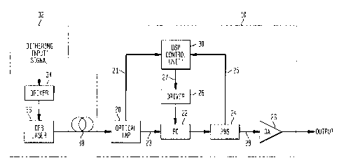
FIG. 1 shows a block diagram of a principal state
polarization (PSP) tracking arrangement 10 for providing
polarization mode dispersion (PNa7) compensation in an
optical transmission system in accordance with the
present invention;
FIG. 2 shows a block diagram of a preferred
arrangement of a digital signal processing control unit
in the principal state of polarization tracking
arrangement of FIG. 1 in accordance with the present
invention;
FIG. 3 graphically shows a spectrum of an electrical
signal illustrating second order harmonics when axes of
the principal state of polarization is not aligned with
axes of a polarization beam splitter in the tracking
arrangement of FIG. 1;
FIG. 4 graphically shows a spectrum of an electrical
signal illustrating a lack of second order harmonics when
axes of the principal state of polarization are aligned
with axes of a polarization beam splitter in the tracking
arrangement of FIG. 1;
FIG. 5 graphically shows an eye-diagram of the
electrical signal of FIG. 3 which include second order
harmonics when the axes of the principal state of
polarization is not aligned with axes of a polarization
beam splitter in the tracking arrangement of FIG. 1; and
CA 02358185 2001-07-06
WO 00/41344 8 PCTlUS99/30616
FIG. 6 graphically shows an eye-diagram of the
electrical signal of FIG. 4 which do not include second
order harmonics when the axes of the principal state of
polarization is not aligned with axes of a polarization
beam splitter in the tracking arrangement of FIG. 1.
Detailed Description
Referring now to FIG. 1, there is shown within a
dashed line rectangle a block diagram of a principal
state polarization (PSP) tracking arrangement 10 for
providing polarization mode dispersion (PNd7) compensation
in an optical transmission system in accordance with the
present invention. The principal state polarization
tracking arrangement 10 comprises an optical tap 20, a
fast polarization controller (PC) 22, a polarization beam
splitter (PBS) 24, an optical amplifier (OA) 26, a driver
28, and a digital signal processing (DSP) control unit
30. The optical tap 20 is coupled to receive a dithering
optical signal from a remote transmitter 32 (shown within
a dashed line rectangle) via a single mode optical fiber
38. The optical tap 20 directs a first portion of the
received optical signal to a first input of the PC 22 via
an optical fiber 23, and directs a remaining second
portion of the received optical signal to a first input
the DSP control unit 30 via an optical fiber 21. The PC
22 is also coupled to receive an electrical feedback
control signal from the driver 28 at a second input
thereof. An output from the PC 22 is coupled to an input
of the polarization beam splitter (PBS) 24. A first
optical output of the PBS 24 is coupled to a second input
of the DSP control unit 30 via an optical fiber 25, and a
second optical output from the PBS 24 is coupled to the
optical amplifier (OA) 26 via an optical fiber 29. An
output from the OA 26 is the output from the PSP tracking
arrangement 10. The remote transmitter 32 comprises a
driver 34 responsive to a dithering input signal for
generating a dithering output driving voltage to a
distributed feedback (DFB) laser 36 in accordance with
the present invention.
CA 02358185 2001-07-06
WO 00/41344 g PCT/US99/30616
In operation, an electrical dithering input signal
is generated at the transmitter 32 which is dithered at a
low speed as, for example, any frequency from 10 KHz to 1
MHz. This electrical dithering input signal is used by
the driver 34 to generate an electrical dithering output
control signal to the DFB laser 36. The DFB laser 36 is
responsive to the electrical dithering output control
signal from the driver 34 for generating a dithering
optical output signal having its frequency dithered at
the above-mentioned low speed for transmission over the
single-mode optical fiber 38. The dithering optical
output signal propagating on optical fiber 38 contains
two orthogonally polarized principal state of
polarizations (PSPs). Due to the path difference that
the two PSPs take over the optical fiber 38, a phase
difference occurs between the PSPs when reaching the PSP
tracking arrangement 10. The general task of the PSP
tracking arrangement 10 is to find the PSPs, and align
them to the axes of the polarization beam splitter (PBS)
24.
In the PSP tracking arrangement 10, the optical tap
20 divides the received dithering optical signal into a
first portion for transmission over optical fiber 21 to a
first input of the DSP Control unit 30, and into a second
portion for transmission over optical fiber 23 to a first
input of the fast polarization controller (PC) 22. The
PC 22 is driven by a feedback control signal received at
a second input thereof which is generated in the DSP
Control unit 30 and provided via the driver 28. It is to
be understood that because of characteristics of the
optical fiber 38, the PSP components are not necessarily
linearly polarized when they arrive at the PSP tracking
arrangement 10, and could be either elliptically or
circularly polarized. The polarization controller 22
transforms the two orthogonal PSP components in the
optical signal received via optical fiber 23 into two
linearly polarized components. Still further, the
polarization controller 22 aligns these linearly
CA 02358185 2001-07-06
WO 00/41344 10 PCT/US99/30616
polarized components to the axes of the polarization beam
splitter (PBS) 24 under the control of the feedback
control signal from the DSP Control unit 30 via the
driver 28. The resulting optical signal from the PC 22
is coupled to an input of the PBS 24 which splits the
linearly polarized components into two separate output
signals. A first output of the PBS 24 is coupled to a
second input of the DSP control unit 31 via optical fiber
25. A second output of the PBS 24 is coupled via an
optical fiber 29 to an input of the optical amplifier 26.
When the two linearly polarized components from the PC 22
are aligned with the axes of the PBS 24, each linearly
polarized component will be coupled to a separate one of
the first and second output of the PBS 24. When the two
linearly polarized components from the PC 22 are not
aligned with the axes of the PBS 24, then a part of each
linearly polarized component will be coupled to a
separate one of the first and second output of the PBS
24. The optical amplifier 26 is responsive to the
optical signal received from the PBS 24 via optical fiber
29 for generating a constant power optical output signal
for transmission to a remote user device (not shown) such
as an optical receiver.
The DSP control unit 30 processes the first and
second input signals from the optical tap 20 and the PBS
24, respectively, and generates a feedback signal to the
PC driver 28 for use by the PC 22. The combination of
the DSP control unit 30, the PC driver 28, and the PC 22
can be referred to as a compensation control means. More
particularly, polarization mode dispersion (PMD) occurs
during optical transmissions over the optical fiber 38.
By dithering the optical transmission signal, information
of the PMD is carried by the dithering portion of the
optical signal. Such dithering signal can be, for
example, sinusoidal or a square wave. Therefore, the
frequency of the transmitted optical signal is increasing
and decreasing and is associated with each PSP since the
PSPs each travel at different speeds down the optical
CA 02358185 2001-07-06
WO 00/41344 11 PCT/US99/30616
fiber 38 and experience some slight phase shift. The
phase shift depends on the amount of PNB7 distortion.
Therefore, by monitoring the interference between the PSP
components in the DSP control unit 30, once the input
signal has been transformed linearly polarized components
by the PC 22, it can be determined whether the axes of
the PSPs are aligned, or not, with the axes of the PBS
24. In response to such determination, the DSP control
unit 30 generates an appropriate feedback control signal
to the PC 22 to reorient and align the linearly polarized
PSP components of the received optical signal to the axes
of the PBS 24.
In the PSP tracking arrangement 10, the polarization
controller (PC) 22 will preferably comprise three
equivalent optical wave-plates to achieve endless
polarization tracking. In such design, there are two
quarter wave-plates (not shown) and one-half wave-plate
(not shown) cascaded in such an order that the half wave-
plate is placed between the two quarter wave-plates.
Although it is possible to achieve arbitrary polarization
transformation using one quarter and one half wave-
plates, it is desirable to use three wave-plates so that
continuous polarization adjustment can be achieved. The
PC 22 can be made of lithium niobate waveguide, squeezed
optical fiber, or liquid crystals. The principles of
operation is the same regardless of what kind of material
is used.
As was stated above, due to the path difference that
the two PSPs take over the optical fiber 38, there will
be a phase difference between the PSPs when reaching the
PSP tracking arrangement 10. After passing through the
PBS 24, the two principle state polarizations (PSPs) will
interfere with each other if the PSPs are not aligned to
the axes of the PBS 24. Since the phase difference is a
function of the frequency of the DFB laser 36 at the
transmitter 32, the interfering laser fields will
oscillate at the dithering frequency. However, if the
PSPs are aligned with the axes of the PBS 24, there is
CA 02358185 2001-07-06
WO 00/41344 12 PCT/US99/30616
one component at each output of the PBS 24, and thus
there is no interference. Therefore, by monitoring the
interference at the DSP control unit 30, the two PSPs can
be aligned to the axes of the PBS 24. To monitor the
interference, a photodetector (shown in FIG. 2) can be
used which measures the intensity of the optical field
received over each of the optical fibers 21 and 25. As a
consequence, the interference signal after the
photodetector will be oscillating at twice the speed of
the laser dithering speed., PSP tracking can then be
accomplished by minimizing the interference component as
will be explained hereinafter.
Referring now to FIG. 2, there is shown a block
diagram of a preferred arrangement of a digital signal
processing (DSP) control unit 30a useful as the DSP
control unit 30 in the principal state polarization (PSP)
tracking arrangement 10 of FIG. 1 in accordance with the
present invention. The DSP control unit 30a comprises
first and second photodiodes 60 and 68, first and second
Analog-to-Digital (A/D) converters 62 and 66, a divider
64, a High Q band pass filter (HIGH Q BPF) 70, a Power or
Amplitude Measuring device (POWER/AMPL. MEASURING) 72, a
Digital Signal Algorithm (DSP ALGORITHM) calculating
device 74, and a Digital-to-Analog (D/A) converter 76.
The output signal from the optical tap 20 (shown in FIG.
1) is coupled to an input of the first photodiode 60. An
output from the first photodiode 60 is coupled to a first
input of the divider 64 via the first A/D converter 62.
The output signal from the Polarization Beam Splitter
(PBS) 24 (shown in FIG. 1) is coupled to an input of the
second photodiode 68. An output from the second
photodiode 68 is coupled to a second input of the divider
64 via the second A/D converter 66. An output of the
divider 64 is coupled to an input of the Power or
Amplitude Measuring device 72 via the High Q bandpass
filter 70. An output from the Power or Amplitude
Measuring device 72 is coupled to an input of a digital
signal processing (DSP) algorithm calculating device 74.
CA 02358185 2001-07-06
WO 00/41344 13 PCT/US99/30616
An output from the DSP algorithm calculating device 74 is
coupled to an input of the digital-to-analog converter 76
which generates an analog control signal at its output
that is coupled to a second input of the PC driver 28
(shown in FIG. 1).
In operation, the signal from the optical tap 20
includes all of the amplitude fluctuations at both the
fundamental and the second harmonic frequencies of the
transmitter's laser dithering frequency, but does not
itself contain interference information. The signal from
the PBS 24 contains two parts, the interference resulting
from the misalignment of the Principle State
Polarizations (PSPs), and the same amplitude fluctuations
as detected by the optical tap 20. In order to use a
high-speed Digital Signal Processing chip, all of the
input signals have to converted from an analog to digital
(A/D) format before any further signal processing occurs.
Many DSP chips have built in A/D and D/A converters.
However, it is necessary in the DSP control unit 30a to
use separate A/D and D/A converters with higher
resolutions. If the laser dithering signal is a single
tone sinusoidal signal, then the signal from the optical
tap 20 will not have frequency components at harmonic
frequencies so that any second harmonic component of the
signal from the PBS 24 has only one contribution, that is
the interference between the PSPs. In this case, the
power or amplitude of the second harmonic component of
signal from the PBS 24 can be used as an error signal to
be fed back to the Polarization Controller (PC) driver 28
in such a way that the error signal is minimized by
reorienting the PSPs in the PC 22. However, the
dithering waveform can be a square wave, as used commonly
for suppression of stimulated Brillouin scattering (SBS).
On the other hand, the polarization dependent loss (PDL)
of the transmission line will cause harmonic distortion,
which interferes with the feedback signal from the PBS
24. The digital divider 64 is used to separate the
harmonic distortion of either the laser dithering
CA 02358185 2001-07-06
WO 00/41344 14 PCT/i1S99/30616
waveform, or the PDL, from the interfering signal of the
two PSPs. Therefore, the output of the divider 64 will
contain only the PSPs interfering information. The high
Q band-pass filter 70 is used to filter out, or pass, the
second harmonic component generated by the interference
of two PSPs. The first and second photodiodes 60 and 69
have built-in, low-noise, amplifiers (not shown) with
low-pass filters (LPFs) (not shown). These photodiode
amplifiers are preferably trans-impedance amplifiers with
a proper gain to drive the,first and second A/D
converters 62 and 66. The photodiode LPFs are used to
reduce the high-frequency noise, and more importantly to
eliminate the high-frequency aliasing effects due to the
digital sampling.
The power or the amplitude of the second harmonic
signal passed by the high Q BPF 70 can be easily
calculated in the digital domain within the
Power/Amplitude Measuring device 72. Digital Signal
Processing has the advantage of fast signal processing,
especially for determining the power or amplitude of a
narrow band sinusoidal signal. An integrator (not shown)
would be used to determine the power if an analog circuit
were used. To achieve reasonable accuracy, many cycles
of integration are necessary, which greatly limits the
response time of over-all Polarization Mode Dispersion
(PMD) compensation. However, a simple DSP algorithm can
accomplish this task with a much faster speed. The steps
of a method for implementing the DSP algorithm are as
follows .
(1) Sending the data stream signal at the output of the
high Q BPF 70 to a buffer (not shown) in the DSP
algorithm device 74.
(2) Retrieving two copies (sets) of the data stream from
the buffer with a delay of 90 degrees between these two
sets of data. In mathematical form, the equations D1 =
Acos(2wt+8), and D2 = Asin(2wt+A) are used, where A is
the amplitude, 8 is the arbitrary phase, and w is the
laser dithering frequency.
CA 02358185 2001-07-06
WO 00/41344 15 PCT/US99/30616
(3) Multiplying D1 by D2, and filtering out the DC
component of the product. This is denoted by the
equation D = (D1)(D2). After a simple calculation, it is
found that D = 0.5A2 + 0.5A2 sin(4wt+28). After
filtering is accomplished, D = 0.5A2, which is the power
of the sinusoidal signal.
The DSP control algorithm for the over-all PSP
tracking is defined by the following steps:
(1) Calculate the power or amplitude of the second
harmonic
component, designated as P-new.
(2) Save it to a new variable, designated as P- old.
(3) Increase (or decrease) the driving signal from the PC
driver
28 (shown in FIG. 2) to the polarization controller
(PC) 22.
(4) Measure P- new again.
(5) If P new > P old, then decrease (or increase) the
driving
signal from the PC driver 28 to the polarization
controller
(PC) 22.
( 6 ) Repeat steps ( 1 ) - ( 5 ) .
In short, the PC driving voltage from the driver 28 is
controlled in such a way that the measured power or
amplitude of the second harmonic signal is always
minimized.
The DSP feedback control unit 30 in the principal
state of polarization (PSP) tracking arrangement 10 is
designed in such a way that both fast response and noise
suppression is achieved using fast digital signal
processing technology. This design does not include any
moving mechanical components, which is very different
from prior art techniques of Polarization Mode Dispersion
(PMD) compensation where mechanical delay lines are used.
Elimination of mechanical delay lines with the present
design makes the tracking arrangement 10 more reliable,
faster, and physically smaller. From an optical
CA 02358185 2001-07-06
WO 00/41344 16 PCT/US99/30616
performance of point of view, it also provides partial
optical noise reduction. Since the amplified spontaneous
emission (ASE) noise is unpolarized, the transmitted ASE
noise will always be reduced by half. However, since
only the more powerful PSP component is selected to pass
through the device, the reduction in its optical power is
always less than half. In other words, there is always
an improvement in the optical signal-to-noise ratio
(OSNR). More particularly, the PSP with the larger
amplitude will automatically be passed through the second
output port of the PBS 24 towards the optical amplifier
26 shown in FIG. 1. This occurs because a second
harmonic received by the DSP Control unit 30 is always
minimized by the DSP Control unit 30 for providing a
feedback control signal to the PC 22. Although the
tracking arrangement 10 is designed to work for a single
wavelength channel, it can be used for any arbitrary
wavelength. In other words, there is no need to provide
a spare or different PMD compensator arrangement for each
wavelength channel. On the other hand, the tracking
arrangement 10 is bit-rate independent. It works for
OC48, OC192, and OC768 transmission systems. This is an
important advantage compared to other techniques where a
different electronic design is required for different
transmission bit-rates.
Referring now to FIGS. 3-6, FIGS. 3 and 4 each
graphically show a typical spectrum of amplitude versus
frequency of electrical signals, and FIGS. 5 and 6 each
graphically show corresponding eye-diagrams of an
arbitrary voltage versus time in picoseconds to
illustrate the principles of operation of the principal
state polarization (PSP) tracking arrangement 10 of FIG.
1. The typical spectrum and eye-diagrams shown
graphically in FIGS. 3-6 are presented for a 10 Gbit/s
transmitter 32 (shown in FIG. 1) which is coupled to a
single mode optical fiber 38 (shown in FIG. 1) with a
Polarization Mode Dispersion (PMD) value of 90 ps. Still
further, the frequency of a distributed feedback (DFB)
CA 02358185 2001-07-06
WO 00/41344 1 ~ PCT/US99/30616
semiconductor laser 36 (shown in FIG. 1) at the
transmitter 32 is dithered at a frequency of 10 KHz. A
polarization controller (PC) 22 (shown in FIG. 1)
comprises three wave-plates, one half wave-plate sitting
between two quarter wave-plates. Each eye-diagram
measurement is obtained at the end of the optical fiber
transmission line 38. FIGS. 3-6 show that full signal
recovery is obtainable with the tracking arrangement 10
of FIG . 1.
More particularly, FIG. 3 graphically shows the
typical spectrum of the electrical signal, assuming a
sinusoidal dithering waveform when the axes of the
principal state polarizations (PSPs) are not aligned with
the axes of the Polarization Beam Splitter 24 (shown in
FIG. 1). The y-axis shows Amplitude (arbitrary unit) and
the x-axis shows frequency (KHz). The frequency of the
DFB laser 36 at the transmitter 32 is dithering at a
frequency of 10 KHz with a peak-to-peak frequency change
of 400 MHz, the bit rate of the transmission is 10
Gbit/s, and the Polarization Mode Dispersion (PMD) value
of the optical transmission link 38 has the above-
mentioned value of 90ps. FIG. 5 graphically shows the
corresponding eye-diagram for the optical output of the
tracking arrangement 10 of FIG. 1 when the axes of the
PSPs are not aligned with those of the Polarization Beam
Splitter 24. The y-axis shows Amplitude (arbitrary unit)
and the x-axis shows Frequency (KHz). The typical
spectrum shown in FIG. 3 shows the second harmonics 90,
and the optical eye-diagram of FIG. 5 shows the
distortion due to PMD, when the axes of the PSPs are not
aligned with those of the Polarization Beam Splitter 24.
In contrast, FIGS. 4 and 6 graphically show the
spectrum of the electrical signal and the eye-diagram
when the axes of the PSPs are aligned with those of the
Polarization Beam Splitter 24 (shown in FIG. 1). No
second order harmonic component appears in spectrum shown
in FIG 4, and the optical eye-diagram is fully recovered
CA 02358185 2001-07-06
WO 00/41344 1 g PCT/US99/30616
in FIG. 6 when implementing the tracking arrangement 10
shown in FIG. 1.
A new method for Polarization Mode Dispersion (PMD)
compensation has been described using a fast PSP tracking
arrangement 10 shown in FIG. 1 which is based on the
interference characteristics of two principal states of
polarization (PSP), and a technique of automatic tracking
of the principal state of polarizations (PSPs). The DSP
feedback control unit 30a shown in FIG. 2 is designed in
such a way that both fast response and noise suppression
is achieved using fast digital signal processing
technology. This arrangement does not include any moving
mechanical components, which is very different from other
techniques of PMD compensation where mechanical delay
lines are used. Elimination of mechanical delay lines of
this design makes the present PSP tracking arrangement 10
more reliable, faster, and smaller. From an optical
performance of point of view, it also provides partial
optical noise reduction. Although the tracking
arrangement 10 is designed to work for a single
wavelength channel, it can be used for arbitrary
wavelength. In other words, there will be no need to
provide a spare or different PMD compensator for each
wavelength channel. On the other hand, the PSP tracking
arrangement 10 is bit-rate independent. The PSP tracking
arrangement 10 works for OC48, OC192, and OC768
transmission systems. This is an important advantage
compared to other techniques where a different electronic
design is required for different transmission bit-rates.
The detection scheme does not depend on the bit-rate, or
the transmission format. It works for 10 Gbit/s, as well
as 40 Gbit/s transmissions, and it works for a Non-
Return-to Zero (NRZ) format, as well as a Return-to-Zero
(RZ) format. Another important feature of the PSP
tracking arrangement 10 is that it can compensate for any
amount of PMD. Normally, the optical delay used by prior
art PMD compensators is the limiting factor for the
maximum allowable PMD value. Since no delay line is
CA 02358185 2001-07-06
WO 00/41344 19 PCT/US99/30616
required in the present tracking arrangement 10, there is
substantially no limit for the PNB7 compensating range.
Due to the simple optical design, the insertion loss can
be made very small so that it can be used without optical
amplification.
In summary, the present PSP tracking arrangement 10
provides the advantages of (1) a simple optical design,
(2) low insertion loss, (3) high compensation speed,
(4) wavelength independence, (5) bit-rate independence,
(6) no limitation on the compensation range for P1~7
values, (7) noise reduction, (8) no mechanical moving
parts, (9) a fast digital signal processing technique,
and (10) transmission format independence.
It is to be appreciated and understood that the
specific embodiments of the present invention described
hereinbefore are merely illustrative of the general
principles of the invention. Various modifications may
be made by those skilled in the art which are consistent
with the principles set forth. For example, digital
signal processing has been described as a preferred use
in the signal processing control unit 30 shown in FIG. 1
because it is very fast. However, where speed is not as
critical, analog signal processing can alternatively be
used to provide the same feedback control signal to the
polarization controller 22.