Note : Les descriptions sont présentées dans la langue officielle dans laquelle elles ont été soumises.
CA 02362174 2001-08-03
WO 00/49485 PCT/US00/03862
Method and Circuit for Receiving Dual Edge Clocked Data
Background of the Invention
Field of the Invention
The present invention relates generally to improvements to computer systems
and, more particularly but not
by way of limitation, to apparatus for receiving data on both edges of a
control signal.
Description of the Related Art
Computer systems commonly include one or more peripheral storage devices that
are used to store andlor
provide access to data. One common type of peripheral storage device is a hard
disk drive. Other types of peripheral
storage devices include tape drives, CD drives (both read-only and
readlwritel, and DVD devices.
The most basic parts of a hard disk drive include at least one platter or
"disk" that is rotated, an actuator
that moves a transducer to various locations over the disk, and electrical
circuitry that is used to write and read data
to and from the disk. The disk drive also includes circuitry for encoding data
so that data can he successfully retrieved
from and written to the disk surface. The circuitry for encoding the data and
circuitry that is used to perform the read
and write operations on the disk are usually in a controller. The controller
can be made as an integrated circuit placed
within the hard disk drive. A disk drive microprocessor ("microprocessor"1 can
be either embedded within or external
to the controller integrated circuit.
The microprocessor controls most of the operations of the disk drive by
configuring and monitoring the
operation of the controller. For example, a host computer can initiate an
operation by sending the controller a read
command. The microprocessor recognizes the command and sets up registers in
the controller to perform the read
operation. The data is then read from the disk into a buffer. When a minimum
amount of data is in the buffer the
microprocessor sets up the controller to send the data from the buffer to the
host.
The process of transferring data from a host to a hard disk typically involves
two steps. First, the data is
moved from a bus, connected to the host, to a data buffer within or coupled to
the disc controller. Second, the data is
transferred from the buffer and to the disk platter by magnetizing areas of
the platter. The first step is generally
referred to as the "external data transfer." The simplest buffer is just an
array of memory cells within the controller.
A buffer may also be an external Dynamic Random Access Memory (DRAMS external
to the controller. The hard disk
controller facilitates this transfer of data from a host bus to the buffer by
using a buffer controller. The buffer
controller includes logic to transfer data to and from the buffer. The
separation between transfers from the host to
the buffer and from the buffer to the platter is used to accommodate the fact
that a sector is usually written or read
as a single unit. In this manner the buffer is used to provide two data rates,
one for data transfers from the system
bus to the buffer, and the other for data transfers from the buffer to the
physical platter.
The host system usually includes a host microprocessor used to control the
operations of the host system.
The host unit would typically include a peripheral device adapter such as an
IDE disk controller to facilitate the
-1-
CA 02362174 2001-08-03
WO 00/49485 PCT/US00/03862
interface between the host system and a storage device. The host system also
includes memory used by the host
during operation.
The external data transfer can be accomplished either as a synchronous or
asynchronous transfer. Digital
circuits in an electronic system are typically controlled by a common clock
signal or by a plurality of clock signals derived
from a common clock signal. Thus, the circuits are "synchronized" with respect
to each other so that a signal generated
by a first circuit in the system can be received by and clocked into other
circuits in the system because the signals
generated by the first circuit have a known phase relationship with respect to
the common system clock signals. The
known phase relationships typically do not exist for circuits that are
controlled by independent clock signals. For example,
peripheral components of a computer system often use independent clocks so
that the peripheral component operates at a
known frequency irrespective of the operating frequency of the computer system
to which it is interconnected. Although
the clock signals of a peripheral component and a computer system may have the
same or similar frequencies, even very
small differences in the clock frequencies cause the phase relationships
between the .clock signals to vary. Thus, the
independent clock signals are "asynchronous" with respect to each other.
Therefore, if a signal is generated by a circuit
controlled by a clock which is asynchronous with the system clock, the signal
cannot be simply provided to the circuits of
the computer system and clocked by the clock signals derived from the system
clock. Rather, the signal must be
synchronized to the system clock before the signal can be applied to the
circuits of the computer system. A
synchronization would be accomplished by providing the same asynchronous
signal received to the circuit output at a
phase and rate used by a local clock. Thus, an asynchronous transfer of data
as opposed to a synchronous transfer,
involves the additional step of synchronizing the data phase to that used by
the receiver. Therefore, a receiving unit in
an asynchronous transfer mode has to provide two functions, one of data
detection, and the other of a data
synchronization. The synchronization of the data transferred is usually
accomplished by sending asynchronous control
signals along with the data to indicate the presence of valid data on a bus.
The ATA (AT-Attachment) or IDE interface is an example of a protocol that
employs asynchronous data
transfers. The ATA interface was originally defined as a standard for embedded
fixed disk storage on IBM ATT""
compatible personal computers. "AT" stands for advanced technology which
referred to the revolutionary, at the time,
16-bit bus used in the ATT"' computer. A DMA (Direct Memory Access) transfer
is an example of an asynchronous
data transfer within the ATA interface. For example, a DMA write operation
would commence with the host writing
an address to an ATA target register of the controller to specify the Logical
Block Address ILBA) of the disk drive
location where data is to be stored. The host then writes a command to a
command register used by the controller to
specify the operation to be performed. For example, a write operation command
may be a "write DMA" command that
is written to the command register. The microprocessor then sets up registers
in the controller according to a
firmware program stored on a ROM. The firmware includes the procedures
followed by the microprocessor when
processing commands in the command register. The procedure can vary depending
on the transfer protocol used.
Once the host sets up the registers, the controller is ready to receive or
provide data. For example, during a
DMA write operation, the host bus controller sends data over by placing data
on the data bus and asserting strobe
-2-
CA 02362174 2001-08-03
WO 00/49485 PCT/US00/03862
signals that correspond to the data placed. The controller will detect the
strobe signals asserted and receive data from
the bus, one segment of data for every strobe detected. The controller also
synchronizes the data to the controller
clock. In this manner the host can send over as much data it wishes without
regard to the clock phase of the target as
long as each piece of data is accompanied by a strobe signal that complies
with the bus specifications.
The rate of data transfer from the bus is governed by the bus specification,
which defines required pulse
widths and rates for the specific interface employed. The ATA-1 standard
requires a minimum cycle time of 480ns for
the write operation. Therefore, when using an ATA-1 bus which is 16 bit wide,
a controller can receive data at a
maximum rate of once every 480ns or 4.1 MBlsec. The ATA-2 and the ATA-3
standards require a minimum cycle time
of 120ns which places a limit of 16.66MBIsec on the data transfer rate. The
standard can be enhanced as to increase
the data transfer rate by reducing the minimum cycle time if termination
devices and new cabling, such as PCI
adapters, are used. However, the different cabling and termination devices are
expensive and not easily installed in
existing systems.
A new standard was adopted that is known as the Ultra ATA or Ultra DMA
protocol. The new Ultra DMA
protocol doubles the previous burst transfer rate of 16.6MB per second to 33
MB per second by allowing data to be
sent during both edges of the strobe signal. In this manner twice as much data
is transferred per strobe cycle without
changing the frequency of the strobe signal, and without the need for
termination devices or different cabling.
To support the Ultra DMA protocol, hard disk controllers need to be able to
receive data sent by the host on
both edges of the strobe signal. ATA processors, for pre-Ultra DMA versions of
the ATA standard, are configured to
receive data on a single edge of the strobe signal. The clock rate for the
controllers is set to enable the receiving of
data on a single edge of a strobe, not both edges. Therefore, controllers have
to employ faster clock rates to keep up
with the faster stream of data coming in. The data from the bus has to be
clocked-in fast enough before it is no longer
valid. The circuit and method of the present invention offers an efficient and
reliable method of receiving dual edge
clocked data without the need for a faster controller clock rate.
Summary of the Invention
The present invention provides a circuit for receiving data sent
asynchronously on both edges of a control
signal. The circuit may be used, for example, in an Ultra DMA controller, or
in another type of device which receives
data according to a dual-edge-clocked asynchronous transfer scheme. An
important benefit of the circuit is that it
allows the dual edge clocked data to be received using substantially the same
controller clock frequency that would be
used if the data were only transferred on a single edge. Thus, for example,
the circuit allows an Ultra DMA controller
to be implemented using the 6.66MHZ controller clock rate commonly used within
ATA-3 controllers.
The circuit includes a strobe generator that generates strobes in response to
the edges of the control signal
accompanying the data. The data from the bus is provided to two temporary
storage units. Data corresponding to a
first edge of the control signal is placed in a first temporary storage unit.
Data corresponding to a second edge of the
-3-
CA 02362174 2001-08-03
WO 00/49485 PCT/LTS00/03862
control signal is placed in a second temporary storage unit. The data is then
synchronously provided to an output by
using the strobes generated by the strobe generator to select either temporary
storage unit to pass data from.
The strobe generator provides pulses in response to both edges of a control
signal while using the same clock
rate used for providing pulses in response to a single edge of the same
control signal. The strobe generator is able to
use a slower clock rate than that needed by a single unit pulse generator by
dividing the tasks of generating pulses
between two sets of components. One set is used to generate pulses for a first
edge, and the other is used to
generate pulses for a second edge.
Additionally, the present invention provides a method of receiving data from a
bus, the data being placed on
the bus on both the rising and falling edges of a control signal. The method
includes generating a synchronous pulse
(synchronized to the controller clock) in response to each transition of the
control signal and passing the data to
temporary storage units such that afl data received along with a first edge of
the control signal is passed to a first unit
and all data received along with a second edge of the control signal is passed
to a second unit. The data is then
provided in synchronism with the controller clock to an output of the
receiving circuit by using the synchronized pulses
to alternate between a selection of data from the two temporary storage units.
The synchronous pulse generator can be constructed from a pair of pulse
generating units connected to the
control line. One of the pulse generation units has its input port inverted.
The pulse generating units can include three
latches. The first latch used to detect the edge of the control signal. The
second latch used to store the response of
the first latch to the edge for a period of one clock cycle. The third latch
used to pass the state of the second latch to
an output, and reset the circuit for one clock cycle such that the resulting
pulse is one clock cycle wide. The system
clock is connected to the second and third latches such that the resulting
pulse is synchronized with the system clock.
Thereby the receiving circuit is used to receive asynchronous data from a dual-
edge-clocked bus and to provide the
data synchronously to a controller data buffer.
Brief Description of the Drawings
The foregoing features and other features of the present invention will now be
described with reference to
the drawings of a preferred embodiment of a disk drive. In the drawings, the
same components have the same
reference numerals. The illustrated embodiment is intended to illustrate, but
not to limit the invention. The drawings
include the following figures:
Figure 1 is a block diagram of a disk drive which embodies the present
invention;
Figure 2 is a block diagram of the receiving circuit included in the disk
controller of Figure 1;
Figure 3, which consists of figures 3A-31, is a timing diagram which
illustrates the operation of the receiving
circuit of Figure 2;
Figure 4, which consists of figures 5A-5H, is a block diagram of 'the strobe
generator circuit included in the
receiving circuit of Figure 2; and
Figure 5 is a timing diagram which illustrates the operation of the strobe
generator of Figure 4.
-4-
CA 02362174 2001-08-03
WO 00/49485 PCT/US00/03862
Detailed Description of the Preferred Embodiment
To facilitate an understanding of the preferred embodiment, the general
architecture and operation of a disk
drive will be described first. The specific architecture and operation of the
preferred embodiment will then be
described with reference to the general architecture and operation of a disk
drive. The disk drive of Figure 1 is an
example of an internal (hard) disk drive included in a computer system. The
host computer and the disk drive
communicate and transfer data via a port 1, which is connected to a data bus
(not shown). In an alternate
embodiment (not shown), the disk drive is an external disk drive which is
connected to a computer via a data bus. In
either case, the data bus is a bus in accordance with an Ultra DMA-ATA
Interface specification. Those skilled in the
art will appreciate that other dual-edge-clocked transfer protocols could be
used, including but not limited to the Ultra
DMA 66 and SCSI protocols, to transfer data between the disk drive and the
computer.
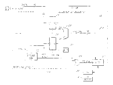
As depicted in Figure 1, the disk drive includes a controller 2 which is
coupled to an ATA port 1, a disk port 3, a
data buffer 4, and a microprocessor 5. The interface 6 serves to connect the
microprocessor bus 66 to the microprocessor
5, for example, an INTEL 80186 or 80188 microprocessor. A ROM which is used to
store firmware code executed by the
microprocessor is omitted from the drawing. The disk port 3 couples the
controller 2 to one or more platters 7, referred to
collectively herein as the "disk." The hard disk controller is using dedicated
clock generator to provide a controller clock
signal on a clock tine (controller clock line) such that the various signals
generated by the components are synchronized.
As is standard in the industry, data is stored on the disk 7 in sectors. Each
sector is byte structured and is made
up of several fields, referred to as the sector format. For example, a typical
sector format includes a fogicat block address
(LBA) of about four bytes followed by a data field of about 512 bytes. The LBA
contains position information, for
example, cylinder, head and sector numbers. The data field is typically
followed by a field for a cyclic redundancy code
(CRC) checksum of about 2-4 bytes. A subsequent field for a number of error
correction code (ECC) bytes, for example
24-40 bytes, is located at the end of the sector.
The controller 2 can be a controller integrated circuit (IC) that comprises
several functional modules which
provide for the writing and reading of disk data. The controller 2 is
connected to the ATA port 1 for a connection to the
ATA bus, and is connected to the disk port 3 for a connection to the disk 7.
The microprocessor 5 is coupled to the
controller 2 via an interface 6 to facilitate the transfer of data, address,
timing, and control information. The data buffer 4
is coupled to the controller 2 via ports to facilitate the transfer of data,
timing, and address information. The interface 6 is
connected to the microprocessor bus 66 to which several modules are connected.
A data flow controller 40 is connected
to the microprocessor bus 66 and to the buffer controller 36. An ECC module 38
and a disk formatter 44 are both
connected to the microprocessor bus 66 and to the buffer controller 36. The
disk formatter 44 is additionally connected
to a data and control port 56 and to the data bus 64. The ATA processor 32 is
connected to the microprocessor bus 66.
The ATA processor 32 is further connected to the buffer controller 36 and to
the data bus 64. The ATA processor 32
receives data and control signals from ports 48 and 46, respectively.
-5-
CA 02362174 2001-08-03
WO 00/49485 PCT/US00/03862
The ATA processor 32 consists primarily of programmable registers and state
machine sequencers that interface
to the ATA port Z6 on one side and to a fast, buffered direct memory access
(DMA) channel on the other side. The ATA
processor 32 also includes a receiving circuit 34 to receive ATA bus data that
is sent on both edges of the Host Strobe (H-
STROBE) signal. The receiving circuit 34 is connected to the buffer controller
36, the data bus 64, and the ATA data port
48. In the preferred embodiment described herein, the ATA processor 32
implements the Ultra DMA protocol.
The disk formatter 44 is a disk interface controller. The disk readlwrite unit
42 includes the disk formatter 44, a
data memory (not shown), the ECC module 38 and a writable control store (WCS)
state machine (not shown). The disk
formatter 44 primarily performs control operations when the microprocessor 5
loads all required control information and
parameter values into a WCS RAM and issues a command. The disk formatter 44
can automatically execute the command
with no further intervention from the microprocessor 5.
The buffer controller 36 can be a four-channel, high-speed DMA controller. The
buffer controller 36 regulates all
data transfers into and out of the data buffer 4. The buffer controller 36
connects the data buffer 4, i.e., an output of its
extended data out (EDO) DRAM, to a disk channel (disk formatter 44), to an ECC
channel (ECC module 38), to an ATA
channel (ATA processor 32), and to the microcontroller bus 66.
Within the buffer controller 36, the DMA controller (not shown) controls
several DMA channels. Each DMA
channel has associated control, configuration and buffer memory address
registers. Communications with the disk and the
ATA bus occurs via disk channels and ATA channels each having a 32-word deep
first-in-first-out (FIFO) memory. The
buffer controller 36 also provides priority arbitration tar buffer resources,
buffer cyclical redundancy check IBCRC), and
automatic refresh control for the DRAM.
The data flow controller 40 serves to reduce data transfer time between the
disk 7 and the controller 2 by
automatically monitoring and controlling the flow of data between the disk and
the ATA channels. This control is
accomplished by reducing the number of interrupts that occur in a typical disk-
to-ATA bus data transfer. When the disk
and the ATA bus data transfer rates are the same, both channels transfer data
at the maximum rate which prevents
slipped sectors in the disk port 3 and periods of inactivity during a data
phase of an ATA bus transfer.
The data flow controller 40 automatically prevents an overflow of the buffer
4, as well as an undertlow of the
buffer 4, by temporarily suspending the disk formatter 44 or the ATA processor
32 before the buffer 4 becomes full or
empty.
Figure 2 illustrates the internal construction of the receiving circuit 34.
The receiving circuit includes a strobe
generator 22 having an input connected to the controller clock line, an input
connected to the H STROBE signal line, and a
pair of output signal lines for the ACK1 and ACK2 signals. A pair of
registers, for example 16 bit registers, are included to
receive the data from the ATA port 1. A first flip-flop 24 has a data input
connected to the data bus 48 of the ATA port 1,
a falling-edge triggered clock input connected to the H STROBE signal line,
and an output connected to an input of a
multiplexer 28. A second flip-flop 24 has a data input connected to the data
bus 48 of the ATA port 1, a rising edge
triggered clock input connected to the H STROBE signal line, and an output
connected to an input of the multiplexer 28.
The multiplexer 28 has an output connected to the data input of a FIFO memory
50, and a select line connected to the
-6-
CA 02362174 2001-08-03
WO 00/49485 PCTlUS00/03862
output of a SET-RESET latch (S-R latch) 52. The S-R latch 52 has a set input
connected to the ACK1 signal line from the
strobe generator 22, a reset input connected to the ACK2 signal line from the
strobe generator 22, and an output
connected to the select line of the multiplexer 28. The FIFO has a data out
port connected to the ATA data bus 48, a data
port connected to the buffer controller 36, and a clock input (FIFO CLK)
responsive to a falling edge of a signal from an OR
gate 54. The OR gate 54 has a first input connected to the ACK1 signal line, a
second input connected to the ACK2 signal
line.
The operation of the circuit of Figure 2 can be more easily understood with
reference to the signal level
illustrations of Figure 3. The signal illustrations of Figure 3 represent the
various signal levels when data is received by the
receiving circuit. When the host sends data to the controller using an Ultra-
DMA protocol, the data is valid on the data bus
on both rising and falling edges of the H STROBE signal generated by the host,
as can be seen from Figures 3B and 3C.
The H STROBE signal can transition at any time relative to the local clock.
The strobe generator 22 (discussed below)
detects the rising edge 502 of the H STROBE signal and generates a pulse on
the ACK2 signal line as illustrated in Figure
3G. The data DO is clocked into flip-flop 26 by the rising edge of the H
STROBE signal as shown in Figure 3E. The ACK2
signal line pulse is also provided to the reset input of the S-R latch 52
which causes the output of the latch to go to a
logical low or 0. The low level output of the S-R latch 52 selects the 0 input
of the multiplexer to pass the contents of the
register 26 to the output FIFO DIN bus as shown in Figure 3H. At the same
time, the ACK2 signal is passed through the
OR 54 gate to provide a clock pulse to the FIFO~CLK signal as shown in Figure
31. The FIFO CLK pulse asserted causes
the data on the FIFO DIN bus to be clocked into the FIFO 50. For the next data
word D1, the strobe generator 22 provides
a pulse on the ACK1 signal line after detecting a falling edge 504 of the
strobe signal of Figure 3B. The data D1
corresponding to the falling edge is clocked into flip-flop 24 as shown in
Figure 3D. The ACK1 signal is then provided to
the set input of the S-R latch 52 which causes the output of the latch to go
to a logical high or 1. The high level output of
the S-R latch 52 selects the 1 input of the multiplexer to pass the contents
of register 24 to the output FIFO DIN bus as
shown in Figure 3H. At the same time, the ACK1 signal is passed through the OR
gate 54 to provide a clock pulse to the
FIFO CLK signal as shown in Figure 31 causing the data D1 to be clocked into
the FIFO 50. This process repeats itself for
every edge of the H STROBE signal until all the data is received.
The strobe generator circuit will now be described with reference to Figure 4.
The circuit includes a first group
of latches 401-403 that are used to generate the ACK1 signal, and a second
group of latches 404-406 that are used to
generate the ACK2 signal. The 401 latch has a data input connected to an
enable line (11CCIENABLE), a falling edge
triggered clock input connected to the H STROBE signal line, a reset port
connected to the output of the 403 latch, and a
data output connected to the input of the 402 latch. The 402 latch has a data
input connected to the data output of the
401 latch, a rising edge clock input connected to the clock signal line, a
reset port connected to the output of the 403
latch, and a data output connected to the input of the 403 latch. The 403
latch has a data input connected to the data
output of the 402 latch, a rising edge triggered clock input connected to the
clock signal fine, and a data output providing
the strobe generator ACK1 line output and connected to the reset ports of the
401 and 402 latches.
CA 02362174 2001-08-03
WO 00/49485 PCT/US00/03862
The second group of latches is configured in the same manner as the first
group with the exception of the first
latch 404 clock input being responsive to a rising edge. The 404 latch has a
data input connected to an enable line
(UCCIENABLE), a falling edge triggered clock input connected to the H STROBE
signal line, a reset port connected to the
output of the 406 latch, and a data output connected to the input of the 405
latch. The 405 latch has a data input
connected to the data output of the 404 latch, a rising edge clock input
connected to the clock signal line, a reset port
connected to the output of the 406 latch, and a data output connected to the
input of the 406 latch. The 406 latch has a
data input connected to the data output of the 405 latch, a rising edge
triggered clock input connected to the clock signal
line, and a data output providing the strobe generator ACK1 line output and
connected to the reset ports of the 404 and
405 latches.
The operation of the circuit of Figure 4 can be better understood with
reference to the signals illustrated in
Figures 5A-5H. The H STROBE signal transitions from a logical low to a logical
high to provide a rising edge 502. The
rising edge 502 causes the output of the 404 latch to change to a high logical
level as is shown in Figure 5F. The output
of the 404 latch is then clocked into the 405 latch on the next rising edge of
the system clock as is shown in Figure 5G.
The output of the 405 latch is clocked into the 406 latch on the next rising
edge of the system clock as is shown in Figure
1 S 5H. The output of the 406 latch then resets both latches 404 and 405
causing their output values to go to a logical low
as is shown in Figures 5F and 5G. The output of the 405 latch is then clocked
into the 406 latch on the next rising edge of
the system clock to provide a low level output as is shown in Figure 5H.
Therefore a pulse is generated on the ACK2 line
in response to a rising edge of the H STROBE signal. The pulse is one clock
cycle wide and is delayed by at least two
clock cycles from the rising edge of the H STROBE signal. The same set of
signal propagation events occur with regards
to latches 401, 402, and 403 when the H STROBE falling edge 504 arrives. As is
shown in Figures 5B, 5C, 5D, and 5E, a
pulse is generated on the ACK1 signal line that is one clock cycle wide, at
most two clock cycles after the H STROBE
falling edge arrives. Each group of latches 401, 402, 403, and 404, 405, 406
is used to generate a pulse to receive data
on a single edge. By combining the two sets, strobes are generated to receive
data on both edges.
From the description above it can be appreciated that dividing the strobe
generation between two units, the first
set of latches 401, 402, 403 and the second set of latches 404, 405, 406,
provides the ability to run the system at a
clock rate with a cycle length that is only one half the minimum H STROBE
width. Only two controller clock cycles need
to fit within the width of the H-STROBE pulse. The advantage of the circuit of
the present invention can be appreciated as
the circuit of the preferred embodiment uses a 66MHZ clock for a 30ns H STROBE
pulse. The ability to use a slower
clock is provided by the division of the pulse generation work between two
distinct units.. No rising edge pulses are
generated in the first set of latches. No falling edge pulses are generated in
the second set of latches.
The two data receiving registers provide additional important advantages to
the receiving circuit. Since the data
is split between the two registers of the circuit of Figure 2, a practical
data rate of '/Z the input data rate is achieved to
provide the receiving circuit with a greater level of data integrity. The data
rate is decreased by selectively providing the
data to two temporary storage units such that a data word is received into and
read from a storage unit on every complete
H STORBE cycle, or every other edge of the H STORBE signal. Data written into
registers needs to be stable some time
_g_
CA 02362174 2001-08-03
WO 00/49485 PCT/US00/03862
prior to and subsequent to the edge it is received on to be properly stored.
Therefore, extending the time the data is
available on the data line usually enhances the integrity of the data in the
storage unit. By selectively passing the data to
two storage units the circuit allows the data more time to settle before it
has to be passed to the FIFO. The data rates
within the receiving circuit can be described as a first high rate, a second
lower rate, and a third higher rate. Data from the
bus is coming in at a high rate, data provided to each individual register is
at a lower rate lone half the bus rate), and data
provided to the FIFO on the FIFO DIN bus is again at a higher rate
(substantially the bus rate).
Another important advantage provided by the separation of data into two
receiving elements is that the data is
on the data line for a longer period of time such that is can be more flexibly
read by the FIFO. By providing the data to two
temporary elements, the data is "stretched" as can be seen from a comparison
of Figures 3C and 3H. The same data is
provided on both the line of Figure 3C and the line of Figure 3H. The
difference between the two is that one is prior to
being received into the registers and the other is after reading from the
registers. The data in Figure 3H remains on the line
longer and is therefore more stable than the data in Figure 3C which allows
the data to be clocked into the FIFO over a
longer, more flexible, period of time.
The receiving circuit can equally be used in the host system to receive data
that is read from the peripheral
device. The peripheral device uses the same strobe signal and data timing when
sending data over to the host system.
Therefore, the receiving circuit described above can be incorporated to a
chipset, or an IC on a host adapter to efficiently
receive dual edge clocked data from a bus.
The receiving circuit can be used for all dual edge clocking protocols
including the Ultra DMA 66 and any future
increased rate protocols.
Although the invention has been described in terms of certain preferred
embodiments, other embodiments
that are apparent to those of ordinary skill in the art are also within the
scope of this invention. Accordingly, the
scope of the invention is intended to be defined by the claims that follow.
-9-