Note : Les descriptions sont présentées dans la langue officielle dans laquelle elles ont été soumises.
CA 02363504 2001-08-17
Hall Sensor With a Reduced Offset Signal
FIELD OF THE INVENTION
The present invention relates to hall sensors and, more
particularly, to hall sensors implemented in a CMOS
technology with an improved contact electrode geometry for
the reduction of the offset signal.
BACKGROUND OF THE INVENTION AND DESCRIPTION OF THE PRIOR
ART
In general, a hall sensor is constructed from an n-doped
active semiconductor area on a p-doped semiconductor
substrate. Usually, the n-doped active area is connected to
an external control logic via four contact electrodes
disposed diagonally opposite in the active area. The four
contact electrodes are divided into two opposite control
current contact electrodes provided to generate a current
flow through the active area and, further, into two
opposite voltage tapping contact electrodes provided to
tap-off a hall voltage occurring perpendicular to the
current flow in the active area as a sensor signal in the
presence of an applied magnetic field.
Usually, in hall sensors with the arrangement described
above, there are two known geometries for the active sensor
area illustrated in Figs. 5 and 6. Fig. 5 shows a square
hall sensor 20 whose contact electrodes 22a - d are
disposed in the corners of the active area 24,
respectively. The shape of the contact electrodes 22a - d
of those of this known hall sensor arrangement is normally
square. During operation of the hall sensor 20, current is
fed between two diagonally opposite contact electrodes 22a,
22c in order to be able to tap-off a hall voltage across
CA 02363504 2001-08-17
-2-
the other two contact electrodes 22b, 22d in the presence
of an applied magnetic field.
Fig. 6 shows a cross-shaped hall sensor arrangement 30 in
the shape of a "Greek cross" in which the rectangular
contact electrodes 32a - d reside at the end of a cross
arm, respectively, wherein the rear boundary of the contact
electrodes 32a - d is identical with the boundary of the
active area 34. The width of the contact electrodes 32a - d
corresponds to the width of the cross arm, i.e., the
contact electrodes 32a - d extend over the whole width of
the active area 34 in the respective cross arm. Analogous
to the square hall sensor, during operation of the cross-
shaped hall sensor, a current is fed between two opposite
contact electrodes 32a, 32c in order to be able to tap-off
a hall voltage across the two contact electrodes 32b, 32d
in the presence of an applied magnetic field.
However, in CMOS processes for the production of
semiconductor structures, inhomogeneties or defects in the
semiconductor material of the active area occur often due
to productional processes. These inhomogeneties cannot be
fully avoided even with expensive production methods. These
inhomogeneties are, however, often a reason for the
ocurrence of an offset of the sensor signal. This means
that at the contact electrodes where a hall voltage is
tapped-off, a sensor signal is detected, even when no
magnetic field is applied to the active area. This
interfering sensor signal is referred to as the offset of
the useful sensor signal or simply as the offset signal. If
those inhomogeneties are in unfavourable positions in the
active area, there can be a relatively high offset signal
in the known hall sensor elements, since the current lines
in the active area can change unfavourably, resulting in a
local high resistance in the active area. Thereby the
offset of the sensor signal occurring at the hall sensor
element depends strongly on the number of inhomogenities
and the position of said inhomogenities.
CA 02363504 2001-08-17
-3-
Due to this strong dependency of the offset signal from the
inhomogeneties in the conventional hall sensor elements,
large exemplary variations occur. Further, the sensitivity
and the measurement accurracy of the hall sensors is
strongly affected. For this reason, an offset compensation
and a correct evaluation of the sensor signals in general,
require very expensive circuit technology.
SUMMARY OF THE INVENTION
It is the object of the present invention to provide an
improved hall sensor element with a reduced offset in the
sensor signal.
The present invention is a hall sensor element having:
an active area and contact electrodes, wherein said contact
electrodes are formed by two opposite 'current supply
contact electrodes between which said active area is
defined for generating a current flow through said active
area and by two opposite voltage-tapping contact
electrodes for tapping-off a hall voltage,
characterized in that
a portion of said respective contact electrodes facing
said active area and being adjacent to said active area has
a geometry that is step-shaped, circular segment-shaped,
elliptic, parabola-shaped, hyperbola-shaped or has a
rectangular extension, in order to reduce the interfering
influence of said contact electrodes on the offset-
reducing effect of the spinning current operation, wherein
all contact electrodes have an identical geometry and are
symmetrically disposed referring to said active area,
respectively and wherein the side length of said contact
electrodes is, at most, 20% of the side length of said
active area.
CA 02363504 2001-08-17
_q_
The present invention is based on the realization that the
offset of the sensor signals occurring in the hall sensor
element can be strongly reduced by the appropriate choice
of geometry of the contact electrodes used. Fundamental for
a small offset of the sensor signal is namely not only a
homogeneous current density distribution of the control
current in ideal conditions in the semiconductor material,
i.e., without inhomogeneties from which the conventional
sensor structures mainly result, but it is of much higher
importance how the current density distribution changes
because of present inhomogeneties or interferences in the
semiconductor material of the active areas and, especially,
at the contacts. At the same time, the resulting offset of
the sensor signals should be as independent as possible
from the position of the inhomogeneties or interferences in
the semiconductor material in order to keep the variations
of the resulting offset values low.
The advantages of the inventive geometries are based on the
following context. The offset that is measurable from the
outside of a hall element depends on three fundamental
factors:
- the strength and extension of the effect in the element;
- the operational voltage at the element, and
- the geometry of the element.
The first two factors are not to be considered any further
in this context. In this case, there is only the geometry
left for changes. The geometry has far-reaching and
numerous influences on the properties of the element. A
special connection exists between the contact geometry and
the offset of the element reduced by the spinning current
explained below.
CA 02363504 2001-08-17
-S-
The spinning current method consists of the fact that the
measurment direction is constantly cyclically turned with a
certain clock frequency by, for example, 90%, i.e., the
operational current flows from one to the opposite contact
electrode, wherein the hall voltage is tapped-off at the
diagonally-opposite contact electrodes, whereupon in the
next cycle, the measurment direction is turned by 90%. The
measured hall voltages are summed-up wherein the offset
voltages should almost cancel each other in one cycle, so
that the portions of the signal that are really magnetic
field dependent are left.
Even in the operation without spinning current, positions
arise dependent on the chosen element and contact geometry
where effects do not interfere and positions where they
cause a large offset. A good example is the connecting line
between the two control current contacts. Due to symmetry
reasons, defects on this connecting line do' not lead to an
offset. As soon as there is a slight deviation from this
line, however, there is immediately a measurable offset at
the hall contacts, although the current densities at both
points are almost identical and not negligibly small.
During the operation with spinning current such a
sensitivity function arises across the location that
describes the effects of a defect at a certain position on
the offset, depending on the geometry. In the case of
finite extended control or hall contacts this function
looks relatively complicated. In a normal hall cross, the
function possesses zero points on the connecting lines
between respectively opposite contacts and, additionally,
between the bisectors of the inner area of the cross . The
remaining contour and thereby especially the extreme values
of this function in the active area can be influenced by
the appropriate choice of element and contact geometry.
Usually, the locations with high relevance for the offset
reside on the edges of the element and the contacts, while
the inner area usually have no new local extreme values.
CA 02363504 2001-08-17
-6-
Since all other properties of the element can also change
due to modification of the geometry, all other properties
need to be considered for changes at the contacts.
In the inventive contacts, the geometry was formed in such
a way that a low offset with high yields and almost
unchanged sensitivity could be achieved.
The effective resolution thereby increases according to the
low offset of the element.
BRIEF DESCRIPTION OF THE DRAWINGS
Preferred embodiments of the present invention will be
described in more detail below with reference to the
accompanying drawings. They show:
Fig. 1 a schematic view of a square hall sensor element
with inventive contact electrodes;
Figs. 2a - a schematic views of the different structures
of the inventive contact electrodes for a square
hall sensor element;
Fig. 3a a schematic view of a cross-shaped hall sensor
element with inventive contact electrodes, and
Figs. 3b - d modified forms of the cross structure;
Figs. 4a - g schematic views of the different structures
of the inventive contact electrodes for a cross-
shaped hall sensor element;
Fig. S a known hall sensor element with a square-active
area and conventional contact electrodes, and
Fig. 6 a known hall sensor element with a cross-shaped
active area and conventional contact electrodes.
CA 02363504 2001-08-17
_7_
DETAILED DESCRIPTION OF THE PREFERRED EMBODIMENTS
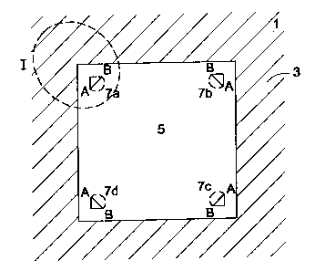
Referring to Fig. 1, the general construction of a
rectangular hall sensor element 1 is illustrated. On a
semiconductor substrate 3, preferably p-doped, a
rectangular-active semiconductor area 5, usually n-doped,
is disposed. In close proximity to the corners of the n-
doped active area 5, contact electrodes 7a - d are disposed
that are usually obtained by a n+ -doping. The contact
electrodes 7a - d are disposed diagonally opposite,
respectively in the n-doped active area 5 surrounded by the
p-doped substrate. The dotted contour of the portions of
the contact electrodes 7a - d facing the active area 5 is
to indicate further different new structures of the contact
electrodes 7a - d that will each be described below in
detail with reference to Figs. 2a - f.
In Figs. 2a - e, the different preferred geometries of the
contact electrodes 7a - d are illustrated. For simplicity
of the following description, only one corner area of the
hall sensor element 1 enlarged to scale with the contact
structure 7a disposed therein (see dotted circle, section 1
in Fig. 1) is illustrated, since the other contact
electrodes 7b - d usually have an identical structure and
are symmetrically positioned in the other corners of the
active area 5. For simplicity of the description, the
contact electrodes 7a - d shown in Figs. 2a - a are
formally separated into two portions, i.e., into one
portion facing the active area 5 and into one portion
turned away from the active area 5. Further, two end points
A and B are defined at the contact electrodes 7a - d
between which the inventive structures of the contact
electrodes 7a - d pass.
In the embodiment of Fig. 2a, the portion of the contact
electrode 7a facing the active area 5 is formed as a
CA 02363504 2001-08-17
_g_
straight line, so that the contact electrode 7a is formed
in the shape of an iosceles triangle.
Fig. 2b shows an embodiment for the structure of the
contact electrode 7a in which the end points A, B of the
portion of the contact electrode 7a facing the active area
are connected staircase or step-shaped so that the
staircase or step-shaped contour of the contact electrode
geometry shown in Fig. 2b is established.
Fig. 2c shows a -contact electrode geometry that has a
circular segment-shaped structure between the end points A,
B curved towards the active area. This curved structure of
the contact electrode can also take an elliptic, parabola-
shaped or a hyperbola-shaped contour.
In Fig. 2d, a contact electrode geometry is shown in which
the portion of the contact electrode 7a facing the active
area has the shape of a isosceles trapezoid, in which the
longer baseline of the trapezoid passes between the end
points A and B of the contact electrode geometry.
In Fig. 2e, a structure of the contact electrode 7a is
illustrated, that is further developed compared to the
structure in Fig. 2d in that the shorter baseline of the
trapezoid facing the active area 5 has a circular segment
shaped, elliptic, parabola-shaped or a hyperbola-shaped
contour that is curved in the direction of the active area.
The above-described contact electrode geometries can also
be approximated by a polygon train for an exact
mathematical description.
It has also been found that the side length of the contact
electrodes should be, at the most, 20g of the side length
of the active area in order to obtain optimum operational
properties of the hall sensor with a significantly reduced
offset signal, i.e., so that the current density
CA 02363504 2001-08-17
-9-
distribution in the active area of a hall sensor is mainly
independent from the position of inhomogeneties or defects
in the semiconductor material.
It should further be noted that the structure of the
portion of the contact electrodes 7a - d turning away from
the active area is not restricted to a triangular contour
as shown in Figs. 2f - f, but can have a shape suitable for
the respective case of application, for example, for
contacting to the exterior or for leading through the
contact electrodes. The contour of the portion of the
contact electrodes 7a - d turning away from the active area
is not essential for the subject of the present invention.
By means of the above-described new structures for the
contact electrodes of a hall sensor element, the
unfavourable offset signals that occur, for example, due to
production induced' inhomogeneties in the semiconductor
material of the active area and superimpose the hall
voltage signal can be reduced. This improvement is achieved
by means of the inventive contact electrode structures in
such a way that the resulting offset signal is mainly
independent from the position of the inhomogeneties or
defects of the semiconductor material. Thereby, exemplary
variations can be reduced and the measurement accurracy of
the hall sensor elements using the above-described novel
contact structures can be improved.
Referring to Fig. 3a, the general construction of a cross-
shaped hall sensor element 10 is illustrated. On a
semiconductor substrate 13, preferably p-doped, a cross-
shaped active semiconductor area 15, usually n-doped, is
disposed. Close to the ends of the cross arms of the active
area 15, contact electrodes 17a - d are disposed that are,
in general, obtained by a n+-class doping. The respective
contact electrodes 17a - d that are provided for generating
a current flow through the hall sensor element and for
tapping-off a hall voltage occurring in the presence of an
CA 02363504 2001-08-17
-10-
applied magnetic field, respectively, are disposed in the
cross arms symmetrically opposite. The dottedcurve of the
portions of the contact electrodes facing the active area
is to indicate, corresponding to Fig. l, further different
new structures of the contact electrodes 17a - d that will
be described below in detail with reference to Figs. 4a -
g.
Naturally, modified cross-elements can be used, wherein the
corners of the element projecting inwardly are varied
according to the examples shown in Figs. 3b - d. Fig. 3d
can thereby be seen as a borderline case to a square
element.
The different preferred geometries of the comact
electrodes 17a - d are illustrated in Figs. 4a - g. For the
simplification of the following description, only one
cross-arm of the hall sensor element 10 with the contact
structure 17a disposed therein is shown in Figs. 4a - g
(see the dotted circular section 2 in Fig. 3a), since the
other contact electrodes 17b - d have an identical
structure and are symmetrically disposed in the other cross
arms of the active area 15. For the simplification of the
description, the contact electrodes illustrated in Figs. 4a
- g are formally separated into two portions, i.e., into a
portion facing the active area and into a portion turning
away from the active area. Further, there are again two end
points, C and D defined between which the inventive
structures of the contact electrodes 17a - d pass.
In the easiest case shown in Fig. 4a, the geometry of the
contact electrode 17a has a rectangular contour wherein the
contact electrode 17a is fully surrounded by n-doped
material.
In Fig. 4b, a further possible contour for the portion of
the contact electrode 17a facing the active area 15 is
CA 02363504 2001-08-17
-11-
illustrated. This contour is formed as a rectangular
extension between the end points C, D.
Fig. 9c shows a contact electrode geometry wherein the
contact electrode 17a between the end points C, D has a
circular segment-shaped contour that is curved towards the
active area. The contour can further be elliptic, parabola-
shaped or hyperbola-shaped.
The geometry of the portion of the contact electrode 17a
facing the active area can further take on a trapezoid-
shaped contour as shown in Fig. 4d, wherein the longer
baseline of the trapezoid coincides with an imaginary
connecting line between the end points C and D.
A structure of the contact electrode 17a is illustrated in
Fig. 4e that is further developed in comparison with the.
structure shown in Fig. 9d in such a way that the shorter
baseline of the trapezoid has a circular segment-shaped,
elliptic, parabola-shaped or hyperbola-shaped contour that
is curved in a direction of the active area.
Further structures of the geometries of the contact
electrodes as they are shown in Figs. 4a - g can be that
the portion of the contact electrode turning away from the
active area extends at least partly up to the p-doped
substrate area. One embodiment of such a structure is
exemplarily illustrated in Fig. 4f. The circular segment-
shaped contour of the contact structure 17a illustrated in
this example between the end points C and D can, however,
also have all other contact electrode curves illustrated in
the Figs. 4a - e.
Further, the whole portion of the contact electrode turning
away from the active area can be disposed adjacent to the
p-substrate as it is shown in Fig. 9g, wherein the width of
the contact electrodes matches the width of the active area
in the cross arm, i.e., the contact electrode 17a extends
CA 02363504 2001-08-17
-12-
across the whole width of the cross arm. The portion of the
contact electrode 17a facing the active area can thereby
have the curves curved towards the active area 15
illustrated in Figs. 4b - e.
It should also be noted that the above-described contact
electrode structures cannot only be used in hall sensor
elements whose active areas have a cross-shaped structure,
but these structures can also be used in hall sensor
elements whose active areas have a star-shaped contour.
Regarding the contact structures described both according
to Figs. 2a - a with reference to rectangular active areas
and contact structures described according to Figs. 4a - g
concerning cross-shaped active areas, it should also be
noted that they can be fully in the n-doped area and only
be connected to the exterior via a metallization level. The
contact areas are, therefore, fully surro~inded by the n-
doped semiconductor area. Apart from that, there is the
possibility that the contact electrodes are not fully in
the active semiconductor area as it ist, for example,
illustrated in Figs. 4g - h. This means that at least a
boundary of the portion of the contact electrode turning
away from the active area can border the boundary of the
active area.
Further, it should be noted that the contact electrodes for
current supply (7a,7c; 17a, 17c) and the contact electrodes
for voltage tapping (7b, 7d; 17b, 17d) have an identical
structure enabling the advantageous use with the so-called
"spinning-current" method for offset compensation. The
advantages of the inventively-designed contacts are
especially noticeable in the spinning current method.
In hall sensors with the conventional contact electrode
structures, the offset voltages that occur due to
inhomogeneties in the semiconductor material will have
different values for each different current flow direction
CA 02363504 2001-08-17
-13-
through the active area, so that no satisfying offset
suppression can be achieved even when using the above-
described compensation method.
By contrast, when using the inventive contact electrode
structures a mainly full offset compensation can be
expected, since the offset reduced effect of the spinning
current operation is far less interferred by the inventive
contacts in comparison to the usual contact geometries.