Note : Les descriptions sont présentées dans la langue officielle dans laquelle elles ont été soumises.
CA 02363766 2001-08-28
WO 00/52518 PCT/US00/05832
PIEZOELECTRIC OPTICAL SWITCH DEVICE
BACKGROUND OF THE INVENTION
1. Field of the Invention
The present invention relates generally to piezoelectric optical switches, and
particularly to planar Mach-Zehnder piezoelectric optical switches having low
birefringence and a high extinction ratio.
2. Technical Background
1 o As the demand for bandwidth increases, so does the drive toward
intelligent,
low-cost, and dynamically-reconfigurable fiber optic networks. To bring this
to pass,
network designers are seeking ways to replace certain network functions that
were
traditionally performed in the electrical domain with solutions in the optical
domain, as
economics and system designs permit. Designers have recognized for quite some
time
t 5 that four port optical devices could find widespread application in fiber
networks to
provide fault tolerance, signal modulation, and signal routing. Integrated
optical
devices using either thermo-optical or electro-optical techniques are
currently available.
However, these devices have drawbacks due to high power consumption and low
switching speeds.
2o Four-port piezoelectric optical devices are of particular interest because
of their
lower power consumption, reduced switching time and adaptability to mass
production
techniques, such as photolithography. One approach that has been considered
involves
an optical phase modulator fabricated by coating a fiber with a thick coaxial
CA 02363766 2001-08-28
WO 00/52518 PCT/US00/05832
piezoelectric lead zirconate titanate film. This circular symmetric in-line
fiber phase
modulator provides phase modulation in a frequency range from 100kHz to 25MHz.
Unfortunately, the efficiency of the device was poor as it exhibited high
attenuation and
low piezoelectricity because of difficulty of depositing a thick PZT film
around an
optical fiber.
In another approach that has been considered, a Mach-Zehnder fabricated from
optical fibers vas used to construct an optical switch. In this design, each
optical fiber
leg was positioned directly on a piezoelectric strip. This design also has
several
drawbacks. First, the piezoelectric strip required high voltage for
commutation.
to Second, the positioning of the strip in relation to the fiber created
asymmetrical stresses
along the fiber axis that perturbed the polarization in the interferometer
arms resulting
in high birefringence and degraded cross-talk performance. As a consequence,
polarized light is required when using this switch.
In yet another approach, a modulator was fabricated by laminating a
piezoelectric strip on a planar waveguide device. The piezoelectric strip was
formed by
sandwiching a layer of piezoelectric material between a lower electrode and an
upper
electrode. The piezoelectric strip was then attached to the overclad of the
device
directly above the waveguide. However, when the piezoelectric strip was
actuated, the
resulting strain vector generated a strong birefringence effect that severely
degraded the
2o extinction ratio at the output of the device.
Thus, a need exists for a four port piezoelectric optical device having
reduced
birefringence characteristics, a high extinction ratio, lower power
consumption, and
reduced switching time. This switch must be cost effective, and its design
suitable for
mass production techniques.
SUMMARY OF THE INVENTION
The present invention is a four port piezoelectric optical switch that
substantially solves the birefringence problem and addresses the other issues
discussed
above. In doing so, the piezoelectric switch of the present invention provides
a high
3o extinction ratio in addition to the lower power consumption and reduced
switching time
possible with piezoelectric switch technology. The planar design of the
present
CA 02363766 2001-08-28
WO 00/52518 PCT/US00/05832
3
invention is well suited for mass production techniques such as
photolithography, and .
offers a promising low-cost solution for some of the signal routing and fault
tolerance
functionality needed to implement an intelligent fiber optic network.
One aspect of the present invention is an optical device for selectively
directing
a light signal in a direction of propagation; the optical device includes a
propagation
path for the light signal and an output. The optical device includes a
piezoelectric
element for directing the light signal into the output by creating a plurality
of mutually
orthogonal strain components in the optical device, wherein the piezoelectric
element is
disposed relative to the propagation path such that only a component of the
plurality of
to mutually orthogonal strain components, aligned in the direction of
propagation, may
substantially exist in the propagation path.
In another aspect, the present invention is a Mach-Zehnder optical device for
directing a light signal having a wavelength ~, in a direction of propagation.
The optical
device includes: a first waveguide having a first propagation path, a
refractive index n,
a first length L1, and a first output, wherein the light signal is propagated
along the first
propagation path; and a first piezoelectric rib for directing the light signal
by creating a
first plurality of mutually orthogonal strain components in the first
waveguide, wherein
the first piezoelectric rib is disposed on the first waveguide at a first
offset from the first
propagation path such that only a component of the first plurality of mutually
orthogonal strain components that is aligned in the direction of propagation
substantially may exist in the first propagation path.
In another aspect, the present invention is a method for directing a light
signal
having a wavelength ~,, in a direction of propagation in an optical
device'including a
first waveguide having a first propagation path, a refractive index n, a first
length L1,
and a first output, wherein the light signal is propagated along the first
propagation
path. The method for directing a light signal includes the steps of: providing
a first
piezoelectric rib for generating a first plurality of mutually orthogonal
strain
components in the first waveguide, wherein the first piezoelectric rib
indisposed on the
first waveguide at a first offset from the first propagation path such that
only a
3o component of the first plurality of mutually orthogonal strain components
that is
aligned in the direction of propagation can substantially exist in the first
propagation
CA 02363766 2001-08-28
WO 00/52518 PCT/US00/05832
4
path; providing a second waveguide disposed adjacent to the first waveguide
having a .
second propagation path, the refractive index n, a second length L2, and a
second
output; and actuating the first piezoelectric rib to selectively deform the
first
waveguide, wherein a first waveguide deformation produces the first plurality
of
mutually orthogonal strain components in the first waveguide.
In another aspect, the present invention discloses a method of fabricating an
optical device~used for directing a light signal. The method of fabricating
includes the
steps of: forming a substrate; disposing a waveguide core layer on~the
substrate;
forming a first waveguide from the waveguide core layer, wherein the first
waveguide
to structure is characterized by a first propagation path, a refractive index
n, a first length
LI, and a first axis, wherein the first axis is substantially perpendicular to
the first
length and the first propagation path; forming a second waveguide structure
from the
waveguide core layer, wherein the second waveguide structure is characterized
by
second propagation path, the refractive index n, a second length L1, and a
second axis
15 parallel to the first axis; disposing a first piezoelectric rib on the
first vaveguide
structure, wherein the first piezoelectric rib has a first rib axis which is
substantially
parallel to the first axis and separated from the first axis by an offset; and
disposing a
second piezoelectric rib on the second waveguide structure, wherein the second
piezoelectric rib has a second rib axis which is substantially parallel to the
second axis
2o and separated from the second axis by the offset, wherein the offset is
selected to
minimize a birefringence in the optical device.
In another aspect, the present invention discloses a method for selectively
directing a light signal into a first output or a second output of an optical
device that
includes at least one waveguide having at least one core connected to the
first output,
25 wherein the light signal propagates along the at least one waveguide in a
direction of
propagation, the method for selectively directing a light signal comprising
the steps of:
providing at least one piezoelectric element for switching the light signal
from the first
output into the second output by inducing a plurality of mutually orthogonal
strain
components in the at least one waveguide, the at least one piezoelectric
element being
3o disposed on the at least one waveguide in a predetermined position such
that only a first
component of the plurality of mutually orthogonal strain components
substantially
CA 02363766 2001-08-28
WO 00/52518 PCT/US00/05832
exists in the at least one core, wherein the first component is a strain
component aligned
to the direction of propagation; and actuating the at least one piezoelectric
element to
thereby generate a deformation in the at least one waveguide causing the
plurality of
mutually orthogonal strain components to be produced in the at least one
waveguide.
Additional features and advantages of the invention will be set forth in the
detailed description which follows, and in part will be readily apparent to
those skilled
in the art from that description or recognized by practicing the invention as
described
herein, including the detailed description which follows, the claims, as well
as the
appended drawings.
l0 It is to be understood that both the foregoing general description and the
following detailed description are merely exerriplary of the invention, and
are intended
to provide an overview or framework for understanding the nature and character
of the
invention as it is claimed. The accompanying drawings are included to provide
a
further understanding of the invention, and are incorporated in and constitute
a part of
15 this specification. The drawings illustrate various embodiments of the
invention, and
together with the description serve to explain the principles and operation of
the
invention.
BRIEF DESCRIPTION OF THE DRAWINGS
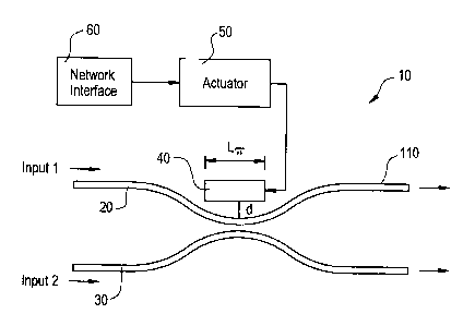
2o Figure 1 is a schematic of a piezoelectric optical switch according to a
first
embodiment of the present invention;
Figure 2 is a detail view of the placement of a piezoelectric rib on a
waveguide
structure in accordance with the present invention;
Figure 3 is a schematic of a piezoelectric optical switch according to a
second
25 embodiment of the present invention;
Figure 4 is a chart showing the relationship between birefringence and the
extinction ratio for the present invention;
Figure 5 is a schematic of a piezoelectric optical switch according to an
alternate
embodiment of the present invention;
3o Figure 6 is a detail view of an etched groove used to mechanically isolate
the
arms of a Mach-Zehnder to reduce cross-talk;
CA 02363766 2001-08-28
WO 00/52518 PCT/US00/05832
Figure 7 is a schematic of a piezoelectric optical switch according to another
alternate embodiment of the present invention;
Figure 8 is a schematic of a piezoelectric optical switch according to another
alternate embodiment of the present invention;
Figure 9 is a schematic of a piezoelectric optical device featuring a variable
attenuation controller according to yet another alternate embodiment of the
present
invention;
Figure 10 is a schematic of a piezoelectric optical device featuring an
optical
modulator according to yet another alternate embodiment of the present
invention; and
1 o Figures 11 A-Q are sequential diagrammatic views of the piezoelectric
optical
switch of the present invention in successive stages of fabrication.
DETAILED DESCRIPTION OF THE PREFERRED EMBODIMENTS
Reference will now be made in detail to the present preferred embodiments of
15 the invention, example of which are illustrated in the accompanying
drawings.
Wherever possible, the same reference numbers will be used throughout the
drawings to
refer to the same or like parts. An exemplary embodiment of the piezoelectric
optical
switch of the present invention is shown in Figure l, and is designated
generally
throughout by reference numeral 10.
2o In accordance with the present invention, an optical device 10 for
directing a
light signal into a desired output includes a piezoelectric rib 40.
Piezoelectric rib 40
directs the light signal by deforming the core of a at least one waveguide to
thereby alter
the optical path length. The deformation creates a three-dimensional strain
vector
having components in each dimension x, y, and z, of a Cartesian coordinate
system. The
25 z-direction corresponds to the direction of propagation. By positioning the
piezoelectric
rib 40 on a waveguide at a predetermined offset position from the core, the
strain
components that are orthogonal to the direction of propagation, x and y, can
be reduced
to a negligible level. Since strains in these directions create bifringence, a
reduction in
these strains will also effect a reduction of the bifringence, as well. The
only remaining
3o strain is in the direction of propagation, and strain in the z-direction
does not create
CA 02363766 2001-08-28
WO 00/52518 PCT/US00/05832
bifringence. The elimination or reduction of bifringence is greatly desired
because
bifringence degrades the extinction ratio at the output of the optical device
10.
Thus, by solving the birefringence issue, the present invention provides an
optical switch that has a high extinction ratio. Another benefit of the
present invention
is its low power consumption and fast switching time, due to the piezoelectric
effect.
In addition, the planar design of the present invention is well suited for
mass production
techniques such as photolithography and thus, offers a promising low-cost
solution for
some of the signal routing and fault tolerance functionality needed in
implementing an
intelligent fiber optic network.
to As embodied herein, and depicted in Figure 1, a schematic of a
piezoelectric
optical switch 10 according to a first embodiment of the present invention
includes a
planar directional coupler 100 formed by waveguide 20 and waveguide 30. A
piezoelectric rib 40 is disposed on waveguide structure 20 at a predetermined
offset
distance "d" away from waveguide core 22 (see figure 2). Piezoelectric rib 40
has a
15 length L~, a distance sufficiently long enough to produce a ~ radian phase
difference
between waveguide 20 and waveguide 30.
As embodied herein, and depicted in Figure 2, a detail view of the placement
of
piezoelectric rib 40 on waveguide structure 20 in accordance with the present
invention
is disclosed. A rectangular coordinate system is provided in Figure 2 as a
convenient
20 means of describing element orientation and will be used throughout.
Piezoelectric rib
40 includes an upper electrode 42 and a lower electrode 44. Electrodes 42 and
44 are
connected to actuator 50. Piezoelectric rib 40 is disposed on overclad 24 of
the
waveguide structure 20 an offset distance "d" from the waveguide axis which
bisects
waveguide core 22. Waveguide structure 20 includes overclad 24 and core 22.
Note
25 that the direction of propagation is in the z-direction.
Waveguide structure 20 and waveguide structure 30 may be of any suitable
well-known type, but there is shown by way of example a waveguide fabricated
using
silica glass with a refractive index of approximately 1.45. One of ordinary
skill in the
art will appreciate that polymers and other like materials may be used. The
geometric
3o shape of core 22 may be either square, rectangular, trapezoidal, or semi-
circular. The
dimensions of the core are dependent on the wavelength of the signal light and
are
CA 02363766 2001-08-28
WO 00/52518 PCT/US00/05832
designed to ensure that the waveguide is single mode at the signal wavelength.
Core 22
is covered by overclad 24 having a thickness that is designed to confine the
mode and
limit propagation losses.
Piezoelectric rib 40 may be of any suitable well-known type, but there is
shown
by way of example, a layer of lead zirconate titanate(PZT) or zinc oxide(Zn0),
having a
thickness in an approximate range of between Sum to 300p.m, a width in an
approximate range of between 20p,m to 300p,m, and a length in an approximate
range of
between 2mm to 3 cm.. The variation in the dimesnions of the piezoelectric rib
are
dependent upon several factors, including the amount of phase shift
piezoelectric rib 40
1 o is required to produce. Piezoelectric rib 40 is produced by spin coating
deposition of a
PZT or Zn0 sol-gel solution and annealing. A more detailed discussion of the
dimensions and placement of piezoelectric rib 40 will be presented
subsequently.
Actuator 50 may be of any suitable well-known type, but there is shown by way
of example, a voltage source capable of supplying two discrete voltages to
piezoelectric
rib 40. The first discrete voltage is on the order of a few volts. The exact
voltage
depends upon the required phase shift. The second voltage level is
approximately
ground. As one of ordinary skill in the art will appreciate , Mach-Zehnders
with perfect
3dB couplers do not exist in practice. Thus, the actual voltage that actuator
50 supplies
to piezoelectric rib 40 may include a bias voltage to compensate for the small
phase
variations generated by imperfections in the Mach-Zehnder. This "tuning" can
done
permanently by UV exposure of the waveguide to perfect the desired phase
difference.
The network interface 60 allows optical device 10 to be adaptable to any
network environment in terms of line levels and logic protocol. Network
interface 60
may also be configured to send fault information back to the network.
The operation of optical device 10 according to the first embodiment of the
present invention as depicted in Figures l and 2, is as follows. In a first
actuation state,
. the network interface receives a command to direct the light signal to the
output of
waveguide 30. Network interface 60 drives actuator SO and piezoelectric rib 40
is de-
energized. A light signal is directed into directional coupler 100 as shown,
and signal
3o power is transferred into waveguide 30. In a second state, the network
interface
receives a command directing optical device 10 to direct all of the light
signal into the
CA 02363766 2001-08-28
WO 00/52518 PCT/US00/05832
9
output of waveguide 20. In response, network interface 60 drives actuator 50
to supply
piezoelectric rib 40 with the appropriate voltage. Piezoelectric rib 40
expands and
deforms waveguide structure 20 to induce a strain in waveguide 20. The induced
strain
caused by the deformation will cause the refractive index and the length of
waveguide
20 to change. Both of these factors contribute to a change in the optical path
length in
waveguide 20. A ~ radian phase difference between waveguide 20 and waveguide
30 is
established and light no longer couples into waveguide 30. As a result,
optical device
is switched and the light signal exits device 10 from waveguide 20. As
discussed
above one of ordinary skill in the art will appreciate that the voltage amount
depends on
to the amount of strain required to produce an index variation that will
generate the
desired phase difference.
The operating principles of the present invention that establish the
relationship
between the dimensions, power requirements, and positioning of piezoelectric
rib 40
with respect to deformation, strain and the resulting phase shift induced in
waveguides
20 and 30 are as follows. If E;" is the field of the input light signal, ~~
the phase
difference between waveguides 20 and 30, and Eo"c the field of the output
signal, one
has the following relationship:
Eour-~ ~'n(1+elnm) (1)
The transmission of Mach-Zehnder 100 is defined as the ratio of the output
intensity
over the input intensity. Thus, from equation ( 1 ) we have:
T _ lou' 1 + cos(~~) ( )
Irn 2
The phase difference 0~ between waveguide 20 and 30 is expressed as:
~~ _ 2~cd (nL) - 2~cL dL
~ (n L + dn) (3)
CA 02363766 2001-08-28
WO 00/52518 PCT/US00/05832
wherein ~, is the wavelength, n is the effective index of the mode propagating
in the
device 10, and L is the length of waveguides 20 and 30 between coupler 112 and
coupler 114. The term d(nL) is the difference of nL between waveguide 20 and
waveguide 30.
s As discussed above, when actuator 50 applies a voltage to piezoelectric rib
40, it
expands or contracts, depending on the .magnitude and polarity of the voltage.
The
expansion and contraction of piezoelectric rib 40 deforms waveguide 20 and
causes a
change in its refractive index and length. The index variation is related ,to
strain by the
following expression:
to
3
dnx = - 2 (P~ » + p~zEy + p~z~) (4)
dnY =- 2 (pu~+ piiEy+ pa~Z) (
wherein nX is the refractive index for light polarized in the x-direction (see
Figure 3), ny
is the refractive index for light polarized in the y-direction, EX, sy, and sZ
= dL/L are
mutually orthogonal strain components in the x, y, and z directions,
respectively. The
2o terms pl and p12 are photoelastic coefficients and vary depending on the
material used
to fabricate the waveguide. The phase difference 0~ between waveguide 20 and
30 is
generally different for the polarization components of the light signal in the
x-direction
and in the y-direction, thus:
3 3 3
D~x = Z~L (- n _ pi m - ~ ~ p~zEy - [ ~ p~z - n)~:) = 2~'L Kx (6)
2 2 2
3 3 3
D~y= 2~(-~ . p~zsr-~ ~ pmy-[n p~z-n]~:)= 2~LKY
2 2 2
CA 02363766 2001-08-28
WO 00/52518 PCT/US00/05832
From equations (6) and (7), the length of piezoelectric rib 40 required to
produce a ~
radian phase difference can be calculated:
Ln = (g)
Kx+Ky
Depending on the material used and the wavelength of the light signal, Ln has
an
approximate range of 2 mm and 3 cm. The acceptable range of widths and
thicknesses
of piezoelectric rib 40 are determined by comparing the strain in the
direction of
propagation eZ, with PZT ribs having various widths and thicknesses, and
waveguide
l0 structures having different overclad thicknesses. Thus, for acceptable
results, the
thickness of the piezoelectric rib 40 has an approximate range of 3~m -300pm
and its
width has an approximate range of 20p,m -300pm. The depth of overclad depends
on
the signal wavelength and must be enough to confine the mode and limit
propagation
losses.
From equations (6) and (7) the polarization dependency of the phase difference
due to the birefringence, is also evident. The main effect of the
birefringence is to lower
the extinction ratio. The extiction ratio refers to the ratio of light in the
output of
waveguide 20, for example, in the "ON" state versus the "OFF" state.
Theoretically,
there should be no light exiting waveguide 20 in the "OFF" state. Thus the
extinction
2o ratio is a measure of light leakage. Obviously, the output of waveguide 30
could also be
used to take the measurement. If the extinction ratio is low, it means that
there is an
excessive amount of light leaking out of device 10 from the output of a
waveguide that
is supposed to be turned off. By lowering the birefringency of the device, one
also
improves the extinction ratio.
Figure 3 is a chart showing the relationship between birefringence and the
extinction ratio. One measure of birefringence is the Q-value. The top curve
shows a
non-birefringent Mach-Zehnder which corresponds to an infinite Q-value. The
bottom
curve shows a device having an extinction ratio of 1 OdB which coiTesponds to
a Q-
value of about five. The Q-value must be higher than 16 to obtain a minimum
3o extinction ratio of 20dB. The Q-value is related to the difference in
refractive indices
for both polarizations by the expression:
CA 02363766 2001-08-28
WO 00/52518 PCT/US00/05832
12
Q - dnx + dnY (9)
dnx - dny
The parameters dnX and dny are index variations produced by stresses induced
by the piezoelectric rib 40. Equations (6) and (7) indicate that the change in
the length
of the waveguide dL/L and the index variation induced by the deformation
compensates
for strain in the direction of propagation, sZ. Thus, birefringence can be
significantly
minimized by eliminating strain components EX and sy in the x and y-
directions,
respectively. This is accomplished by the present invention by disposing
piezoelectric
1o rib 40 at a predetermined offset distance from the central axis of core 22
(see Figure 3)
and the path of propagation. At the time of actuation, the geometric position
of the
piezoelectric rib acts to minimize strain components sx and Ey; however,
switching
functionality is retained by using sZ to vary the index and the length of the
waveguide.
The optimum range for the offset distance was determined by mapping the Q-
value (inversely proportional to birefringence) as a function of the offset
distance using
a Mach-Zehnder having a PZT rib having length Ln, a width of approximately
100p,m,
and a thickness of 20pm. Under these conditions the optimal value for the
offset
distance in this configuration is approximately 100pm. Generally speaking, the
offset
distance is approximately equal to ~./4n.
2o As embodied herein, and depicted in Figure 4, a schematic of piezoelectric
optical switch 10 according to a second embodiment of the present invention
includes a
planar Mach-Zehnder 100 formed by waveguide 20 and waveguide 30. A
piezoelectric
rib 40 is disposed on waveguide structure 20 an offset distance "d" away from
the
waveguide core 22 (see Figure 2). Piezoelectric rib 40 has a length equaling
Ln.
Piezoelectric rib 40 is electrically connected to actuator 50. Actuator 50 is
connected to
network interface 60, which receives network commands and drives actuator SO
accordingly.
The operation of optical device 10 according to the second embodiment of the
present invention as depicted in Figure 4, is as follows. In a first actuation
state, the
3o network interface receives a command to direct the light signal to the
output of
CA 02363766 2001-08-28
WO 00/52518 PCT/US00/05832
13
waveguide 30. Network interface 60 drives actuator 50 and piezoelectric rib 40
is
deenergized. A light signal is directed into Mach-Zehnder 100 as shown. Half
of the
light signal is coupled into waveguide 30 by 3dB coupler 112. As one ordinary
skill in
the art will appreciate, a symmetric Mach-Zehnder with perfect 3dB couplers
operates
in a cross state when no phase difference exits between waveguides 20 and 30
arid the
light signal will exit device 10 from the output of waveguide 30.
In a second state, the network interface receives a command directing the
light
signal to exit optical device 10 from the output of waveguide 20. In response,
network
interface 60 drives actuator 50 to supply piezoelectric rib 40 with the
voltage necessary
l0 for inducing a ~ radian phase difference. Piezoelectric rib 40 expands and
deforms
waveguide structure 20 inducing a strain in waveguide 20. The induced strain
caused by
the deformation will cause the refractive index and the length of waveguide 20
to
change. Both of these factors contribute to a change in the optical path
length that the
light signal follows when propagating in waveguide 20. One ordinary skill in
the art
15 will appreciate that the amount of voltage required depends on the amount
of strain
required to produce an index variation that will generate the desired phase
difference.
The phase difference determines the size of the electric field required to
drive
piezoelectric element 40. The voltage supplied to piezoelectric rib 40
establishes a ~t
radian phase difference between waveguide 20 and waveguide 30. As a result
optical
2o device 10 is switched and the light signal exits device 10 from waveguide
20.
In a third embodiment of the invention, as embodied herein and as shown in
Figure S, a schematic of piezoelectric Mach-Zehnder optical switch 10 includes
a planar
Mach-Zehnder 100 formed by waveguide 20 and waveguide 30. A piezoelectric rib
40
is disposed on waveguide structure 20 offset a distance "d" away from the
waveguide
25 20. Another piezoelectric rib 70 is disposed on waveguide structure 30 also
offset a
distance "d." Piezoelectric ribs 40 and 70 could also be disposed on the
interior sides of
waveguides 20 and 30, respectively. Note that Figure 2 and the discussion of
offset
distance "d" applies to this embodiment as well as the first embodiment.
Piezoelectric
rib 40 is electrically connected to actuator SO and piezoelectric rib 70 is
electrically
3o connected to actuator 52. Actuators 50 and 52 are driven in tandem by
network
interface 60.
CA 02363766 2001-08-28
WO 00/52518 PCT/US00/05832
14
It will be apparent to those of ordinary skill in the pertinent art that
modifications and variations can be made to piezoelectric ribs 40 and 70
depending on
the amount of phase shift each rib is required to provide. In the second
embodiment of
the present invention, the switching functionality is distributed between
waveguides 20
and 30 by placing a second piezoelectric rib 70 on waveguide 30. As in the
first'
embodiment, a total phase difference of ~ radians between waveguides 20 and
waveguide 30 must be provided to switch the light signal into the output of
waveguide
20. However, using piezoelectric rib 70 enables the use of a "push-pull"
effect wherein
piezoelectric rib 40 provides a positive phase shift and piezoelectric rib 70
provides a
to negative phase shift. Thus, piezoelectric rib 40 must provide a +~/2 radian
phase shift
and piezoelectric rib 70 must provide a -~/2 radian phase shift. Since the
phase shift
each piezoelectric rib is required to provide has been reduced from ~ radians
to ac/2
radians, the length of each rib can also be reduced by approximately a factor
of two:
t5 L = al, (10)
1~+KY
where a - 0.5. To avoid problems associated with mechanical cross-talk,
piezoelectric
ribs 40 and 70 should be separated by a minimum distance of SOOp,m. The
recommended separation range is between SOOpm and 1000p.m. This is a trade off
2o between the size of the device and cross-talk.
As embodied herein, and depicted in Figure 6, an alternate embodiment of the
present invention may include an etched groove 80 between waveguide 20 and
waveguide 30. The etched groove 80 is provided to reduce the mechanical cross-
talk by
isolating arms 20 and 30 of the Mach-Zehnder 100.
25 The operating principles of the present invention that establish the width,
thickness, power requirements, and positioning of piezoelectric ribs 40 and 70
with
respect to the strain and phase shift induced in waveguides 20 and 30 are
essentially
identical to those discussed above with respect to the first embodiment
depicted in
Figures 1 and 2.
CA 02363766 2001-08-28
WO 00/52518 PCT/US00/05832
The operation of optical device 10 according to the third embodiment of the
present invention as depicted in Figure 5 is as follows. In a first actuation
state, the
needs of the network require that the light signal directed into the output of
waveguide
30. Half of the light signal entering Mach-Zehnder 100 is coupled into
waveguide 30
by 3dB coupler 112. A symmetric Mach-Zehnder with perfect 3dB couplers 112 and
114 will operate in a cross state when no phase difference exits between
waveguides 20
and 30 and the light signal will the output of waveguide 30. Thus, upon
processing the
network command, network interface 60 drives actuators 50 and 52 and the
voltage
supplied to piezoelectric ribs 40 and 70 drops to approximately zero volts. As
to discussed above and as one of ordinary skill in the art will appreciate,
Mach-Zehnders
with perfect 3dB couplers do not exist in practice. At each switch state,
actuators 50
and 52 supply piezoelectric ribs 40 and 70, respectively, with the nominal
voltages plus
small bias voltages to compensate for the small phase variations generated by
the
imperfections of the Mach-Zehnder.
15 In a second actuation state, the newtork interface is commanded to direct
the
light signal into the output of waveguide 20. Network interface 60 drives
actuators 50
and 52 accordingly. Actuator 50 supplies a positive voltage to piezoelectric
rib 40 and
actutor 52 supplies a negative voltage of approximately the same magnitude to
piezoelectric rib 70. Piezoelectric rib 40 will expand when deforming
waveguide
2o structure 20. Piezoelectric rib 70 will contract when deforming waveguide
structure 30.
The deformations strain waveguides 20 and 30 and thereby change their path
lengths.
The path length variation in waveguide 20 results in approximately a +~/2
radian phase
shift whereas the path length variation in waveguide 30 yields approximately a
-~c/2
radian phase shift. Thus, a ~ radian phase difference, or an odd multiple of ~
radions,
between waveguide 20 and waveguide 30 is established and the light signal is
directed
into the output of waveguide 20. Of course the polarities of the voltages
could be
reversed to yield the same results. However, the voltages must have opposite
polarities.
In another alternative embodiment of the present invention, as embodied herein
and as shown in Figure 7, piezoelectric rib 40 consists of an outer
piezoelectric strip 46
disposed on an exterior side of waveguide 20, and inner piezoelectric strip 48
disposed
on an interior side of waveguide 20. Piezoelectric rib 70 consists of outer
piezoelectric
CA 02363766 2001-08-28
WO 00/52518 PCT/US00/05832
16
strip 72 disposed on an exterior side of waveguide 30, and inner piezoelectric
strip 74
disposed on an interior side of waveguide 30. Inner piezoelectric strip 48 and
inner
piezoelectric strip 74 are separated by a minimum of SOO~m, the distance being
within
the recommended separation range between SOO~,m and 1000~.m, as discussed
above
and shown in Figure 7. This is a trade off between cross-talk and device size.
The
etched groove shown in Figure 6 could also be used in this embodiment.
Actuator 50 is
connected to piezoelectric strips 46 and 48, supplying them with identical
voltages.
Actuator 52 is connected to piezoelectric strips 72 and 74, supplying them
with
identical voltages. Network interface 60 is connected to actuator SO and
actuator 52,
1 o and it drives then in tandem.
It will be apparent to those of ordinary skill in the pertinent art that
modifications and variations can be made to piezoelectric ribs 40 and 70 of
the present
invention depending on the amount of phase shift each is required to provide.
By
placing piezoelectric strips 46, 48, 72 and 74 on both sides of their
respective
15 waveguides 20 and 30, the length of the piezoelectric ribs can be reduced
by a factor of
two with respect to the second embodiment and a factor of four with respect to
the first
embodiment. Thus, in equation (10), a = 0.25.
With the exception of the variations discussed above, optical switch 10 in
Figure 7 operates in the same way as the embodiment depicted in Figure 5 and
thus, a
2o description of its operation will not be repeated.
In yet another alternative embodiment, as embodied herein and as shown in
Figure 8, a schematic of piezoelectric optical switch 10 includes Mach-Zehnder
100
formed by waveguide 20 and waveguide 30. Piezoelectric rib 40 is disposed on
waveguide structure 20 with an offset distance from the waveguide core 22.
Another
25 piezoelectric rib 70 is disposed on waveguide structure 30 also disposed an
offset
distance from the core. The discussion of offset distance with respect to
Figure 2
applies to this embodiment, as well. Piezoelectric rib 40 is electrically
connected to
actuator 50. Piezoelectric rib 70 is electrically connected to actuator 52:
Actuators SO
and 52 are connected to, and driven in tandem by, network interface 60.
30 Actuator 50 and actuator 52 may be of any suitable well-known type, but
there
is shown by way of example, a voltage source capable of supplying three
discrete
CA 02363766 2001-08-28
WO 00/52518 PCT/US00/05832
17
voltages to piezoelectric rib 40 and piezoelectric rib 70. This embodiment
uses a "push-
pull" effect similar to the technique discussed above with respect to an
earlier
embodiment. Commutation is effected by driving piezoelectric rib 40 and
piezoelectric
rib 70 with voltages having opposite polarities. Thus, the voltage sources
operate in
tandem such that actuator 52 supplies -V volts when actuator 50 supplies +V
volts.
When actuator SO supplies -V volts, actuator 52 is supplying +V volts. When
actuator
50 is at approximately ground, so is actuator 52. As discussed above, the
nominal
voltage V, is dependent on a variety of factors, such as the desired phase
difference and
size of the piezoelectric rib. It will be apparent to one of ordinary skill in
the pertinent
to art, that multiple voltage combinations may be used to split the light
signal between
waveguides 20-and 30 as desired.
It will be apparent to those of ordinary skill in the pertinent art that
modifications and variations can be made to the present invention depending on
the
amount of phase shift each rib is required to provide. In Figure 8, waveguide
20 is
shorter than waveguide 30 by a distance ~L= L2-L1, which is approximately
250~m
when ~. = 1.55 p.m and n -1.5. This path length difference between waveguide
20 and
waveguide 30 establishes a ~/2 radian phase difference between waveguide 20
and
waveguide 30. Thus, in order to obtain either n radian phase shift or zero
phase shift
between waveguides 20 and 30, each of piezoelectric elements 40 and 70 are
only
2o required to produce a ~c/4 radian phase shift. Because the phase shift
piezoelectric rib 40
and piezoelectric rib 70 must provide has been reduced from ~ radians to ~/4
radians,
the length can also be reduced by approximately a factor of four. Thus,
equation (10)
can be used to calculate the lengths Lt,~4~, of piezoelectric rib 40 and
piezoelectric rib
70, where a = 0.25. One of ordinary skill in the art will also recognize that
this
embodiment can be iwplemented using one piezoelectric rib or four
piezoelectric ribs.
It will be apparent to those of ordinary skill in the pertinent art that
modifications and variations can be made to the present invention depicted in
Figure 8.
Instead of designing the path length difference to provide a n/2 radian phase
difference,
the path length difference can be designed to provide a permanent ~ radian
phase
3o difference. In this case, when the piezoelectric ribs are not actuated,
optical device 10
CA 02363766 2001-08-28
WO 00/52518 PCT/US00/05832
18
is in the bar state rather than in a cross-state. This design is of interest
when it is more
probable that the switch will be used in the bar state rather than the cross-
state.
As discussed above with respect to an earlier embodiment, to avoid problems
associated with mechanical cross-talk, piezoelectric ribs 40 and 70 should be
separated
by a minimum distance of 500p.m. The recommended separation range is between
SOO~m and 1 OOO~tm. As discussed above, the separation range is a trade-off
between
cross-talk and device size. The etched groove shown in Figure 6 can also be
used in this
embodiment.
The operation of optical device 10 according to the invention as depicted in
1 o Figure 8 is as follows. In a first actuation state, the network commands
optical device
to direct the light signal into the output of waveguide 20. Network interface
60
drives actuators 50 and 52 accordingly. Actuator 50 supplies a positive
predetermined
voltage to piezoelectric rib 40. Actuator 52 applies a negative voltage of the
same
magnitude to piezoelectric rib 70. Piezoelectric rib 40 deforms waveguide 20
and
approximately a ~c/4 radians phase shift is generated. Piezoelectric rib 70
deforms
waveguide 30 and approximately a -~/4 radians phase shift is generated. As one
of
ordinary skill in the art will recognize, the actual phase shifts are
dependent upon the
inherent imperfections in the MZ1. The phase variation may be slightly
different on
each one. The requirement is that a total phase difference of n radians is
established
2o between waveguide 20 and waveguide 30. Upon doing so, optical device 10 is
commutated and the light signal exits the device from the output. of waveguide
20.
In a second actuation state shown in Figure 8, actuator SO and 52 supply
approximately zero volts to their respective piezoelectric ribs, 40 and 70. As
discussed
above, the asymmetric Mach-Zehnder in Figure 8 is fabricated having an
inherent phase
difference of approximately ~/2 radians between waveguide 20 and waveguide 30.
Thus, when piezoelectric ribs 40 and 70 are not deforming waveguides 20 and
30,
respectively, the inherent ~/2 radian phase difference causes the light signal
to be
equally split between the outputs of waveguides 20 and 30. In this state, the
optical
device 10 is a 3dB splitter.
CA 02363766 2001-08-28
WO 00/52518 PCT/US00/05832
19
In a third actuation state, the network interface 60 is commanded to direct
the
light signal into the output of waveguide 30. Network interface 60 drives
actuator 50 to
supply piezoelectric rib 40 with a negative voltage. In similar manner,
actuator 52
supplies piezoelectric rib 70 with a positive voltage of approximately the
same
magnitude. Piezoelectric rib 40 deforms waveguide 20 and generates
approximately a
-~/4 radian phase shift. Piezoelectric rib 70 deforms waveguide 30 and
approximately a
+~/4 radians phase shift is generated. In this actuation state, the phase
shifts generated
by piezoelectric ribs 40 and 70 cancel the inherent ~/2 phase difference
between
waveguide 20 and waveguide 30 caused by their path length difference. Thus, no
phase
to difference exists between waveguide 20 and waveguide 30 and the light
signal is
directed into the output of waveguide 30 as commanded.
In yet another alternative embodiment, as embodied herein and as shown in
Figure 9, a schematic of piezoelectric variable attenuator 10 includes a Mach-
Zehnder
100 formed by waveguide 20 and waveguide 30. Piezoelectric rib 40 is disposed
on
1 s waveguide structure 20 an offset distance from the waveguide core 22. The
discussion
of the offset distance with respect to Figure 2 equally applies to this
embodiment, as
well. Piezoelectric rib 40 is electrically connected to actuator 50.
Actuator 50 may be of any suitable well known type, but there is shown by way
of example, a variable voltage source for dynamically varying the voltage over
a
2o continuous range of voltages. One of ordinary skill in the art will
appreciate that the
power level of the light signal in the output of either waveguide 20 or 30 is
dynamically
controlled in proportion to voltage level supplied by actuator 50. Thus,
variable
attenuator 10 is implemented by varying the voltage over a continuous range.
The operation of variable attenuator 10 according to the invention as depicted
in
25 Figure 9 is as follows. As discussed with respect to the first embodiment,
if
piezoelectric rib 40 is de-energized, the light signal propagating in a
symmetric Mach-
Zehnder 100 will be directed into the output of waveguide 30. When a command
is
received ordering that the light output from waveguide 30 be attenuated to a
certain
level, network interface 60 interprets the command and translates it into a
voltage level
3o within the range provided by actuator 50. Actuator 50 supplies
piezoelectric rib 40 with
the voltage level as ordered. In response, piezoelectric rib 40 expands and
deforms
CA 02363766 2001-08-28
WO 00/52518 PCT/tJS00/05832
waveguide structure 20, causing the refractive index and the length of
waveguide 20 to
change. Thus, a portion of the light signal is diverted from the output of
waveguide 30
and redirected into the output of waveguide 20. As the voltage is increased
more of the
signal is diverted from waveguide 30 and is thereby attenuated. When actuator
50
5 supplies the predetermined voltage to piezoelectric rib 40 a ~ radian phase
difference
between waveguide 20 and waveguide 30 is established. In this state, the
output from
waveguide 30 is completely attenuated. Thus, the voltage supplied by 'actuator
50 is
proportional to the attenuation amount.
In yet another alternative embodiment, as embodied herein and as shown in
to Figure 10, a schematic of piezoelectric tunable filter 10 includes a Mach-
Zehnder 100
formed by waveguide 20 and waveguide 30. Note that waveguide 20 is shorter
than
waveguide 30 by a distance OL= L2-L,, which is approximately 200 p,m.
Piezoelectric
rib 40 is disposed on waveguide structure 20 an offset distance from the
waveguide
core 22. The discussion of the offset distance with respect to Figure 2
equally applies
15 to this embodiment, as well. Piezoelectric rib 40 is electrically connected
to actuator
50.
The operation of tunable filter 10 according to the invention as depicted in
Figure 10 is as follows. The phase variation between the two arms is given by
the
following equation:
0~ _ ~ nOL ( 11 )
Since the refractive index n is wavelength dependent, the product nOL is also
wavelength dependent. For a large DL, a large phase difference may be
obtained.
between different wavelengths. For example, in a first actuation state wherein
piezoelectric rib 40 is not actuated, there is no phase difference for light
at ~,1= 1554.5
nm and a ~ phase difference exists for light at ~,2 = 1558.5 nm. Thus, ~,,
won't be
interferred with, whereas ~,2 will experience destructive interference. In a
second
actuation state, piezoelectric rib 40 induces a ~ phase difference between
waveguide 20
3o and waveguide 30. Because of the wavelength dependency discussed above, the
CA 02363766 2001-08-28
WO 00/52518 PCT/US00/05832
21
attenuation at the different wavelengths will change and ~,2 won't be
interferred with
and ~.i will be destroyed by destructive interference.
Figures 11 A-Q are sequential diagrammatic views of the piezoelectric optical
switch of the present invention in successive stages of fabrication. In Figure
1 lA
substrate 100 is formed. Substrate 100 may be of any suitable well known type,
but
there is shown by way of example a substrate formed of silicon glass. Figure
11 B
shows buffer layer 112 being deposited on substrate 100. Buffer layer 112 may
be of
any suitable well known type, but there is shown by way of example a layer
formed of
silica glass. Figure 11 C shows core layer 114 being deposited on buffer layer
112. Core
layer 114 may be of any suitable well known type, but there is shown by way of
example a layer formed of silica glass having a~~refractive index n, higher
than that of
the buffer layer 112. One of ordinary skill in the pertinent art will
appreciate that the
fabrication steps described in Figures 1 lA-11C can also be realized using
polymers,
copolymers, monomers or other suitable materials. Figures 11D and 11H show the
photolithographic process of forming waveguide structure 20 and waveguide
structure
30. Mask 116 is positioned over core layer 114 and the pattern of waveguide
structures
and 30 are,transferred to the core layer 114 by illumination of the mask. The
etching
process shown in Figure 11G removes excess core material. In Figure 11H
overclad
layer 24 is deposited over waveguide structures 20 and 30. Figures 11I-11N
show
2o piezoelectric rib 40 being formed on waveguide structure 20. A layer of PZT
or Zn0 is
deposited on bottom electrode 44.The dimensions of the PZT rib will vary
within the
ranges provided in the discussion above. In Figure 11 P pigtails 18 are
connected to
waveguides 20 and 30 to provide optical connectivity. Finally, in Figure 11Q,
the
piezoelectric rib electrodes are wired to a connector disposed in the
packaging optical
unit 118.
It will be apparent to those skilled in the art that various modifications and
variations can be made to the present invention without departing from the
spirit and
scope of the invention. Thus, it is intended that the present invention cover
the
modifications and variations of this invention provided they come within the
scope of
3o the appended claims and their equivalents.