Note : Les descriptions sont présentées dans la langue officielle dans laquelle elles ont été soumises.
CA 02365209 2010-06-15
11280-01 CA Patent
Method for Micro-Fabricating a Pixelless Infrared Imaging Device
Field of the Invention
[11 This invention relates to infrared thermal imaging devices and in
particular to micro-
fabrication of pixelless infrared thermal imaging devices comprising
epitaxially
integrated quantum well infrared photodetector and light emitting diode.
Background of the Invention
[21 Infrared imaging is widely used in a variety of applications including
night vision,
surveillance, search and rescue, remote sensing, and preventive maintenance,
to name a
few. Imaging devices to provide these applications are typically constructed
of HgCdTe
or InSb focal plane arrays. These focal plane arrays are known to be pixel
mapped
devices, where an array element is generally mapped to one or more circuit
elements.
However, such focal plane arrays are difficult to manufacture and expensive.
Quantum
Well Infrared Photodetectors (QWIPs) are able to detect Mid to Far InfraRed
(M/FIR)
light, providing an output current as a result. However, such devices have not
been able
to be successfully used in efficient and inexpensive image detectors. The
basic idea of
QWIPs using intraband or intersubband transition for M/FIR detection have been
disclosed in U.S. Patent 4,205,331, issued May 27, 1980 to Esaki et al. and in
U.S. Patent
4,873,555, issued Oct. 10, 1989, to Coon et al. Embodiments of QWIPs using
intraband
or intersubband transitions have been disclosed in U.S. Patent 4,894,526,
issued Jan.16,
1990, to Bethea et al. and U.S. Patent 5,023,685, issued June 11, 1991 to
Bethea et al.
The latter two patents describe a device having improved efficiency by
utilizing a series
of quantum wells.
[31 An improvement of these earlier technologies was disclosed by one of the
present
inventors, H. C. Liu, in U.S. Patent 5,567,955, issued Oct. 22, 1996, to the
National
Research Council of Canada, , wherein the vertical integration of a Light
Emitting Diode
(LED) with a QWIP is described. The QWIP-LED is a photon frequency up-
conversion
device, The device comprises either a photo-diode or a photo-conductor
connected in
series with a LED. The photo-diode or the photo-
s
CA 02365209 2010-06-15
11280-01 CA Patent
conductor acts as a M/FIR detector, whereas the LED emits in the NIR or the
visible
spectrum. A forward constant bias is applied to the LED with respect to the
QWIP. A
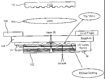
MIFIR excitation of the detector decreases its resistance and thereby
increases the voltage
dropped across the LED, leading to an increase in the LED emission intensity.
Therefore,
the incoming M/FIR radiation has been converted into an increase of the NIR or
visible
emission. The emission in the NIR is efficiently detected by a Si Charge-
Couple Device
(CCD), resulting in a highly efficient detector. The vertical integration
results from
epitaxial deposition of the LED material over the QWIP materials.
[41 Details about the QWIP-LED technology as well as numerous embodiments are
disclosed in the following references:
U.S. Patent 5,646,421, issued Jul. 8, 1997, to H. C. Liu;
U.S. Patent 6,028,323, issued Feb. 22, 2000, to H. C. Liu;
H.C. Liu, L.B. Allard, M. Buchanan, Z.R. Wasilewski, "Pixelless infrared
imaging device", Electronics Letters 33, 5 (1997);
L.B. Allard, H.C. Liu, M. Buchanan, Z.R. Wasilewski, "Pixelless infrared
imaging utilizing a p-type quantum well infrared photodetector integrated with
a light
emitting diode", Appl. Phys. Lett. 70, 21 (1997);
E. Dupont, H.C. Liu, M. Buchanan, Z.R. Wasilewski, D. St-Germain, P.
Chevrette, "Pixelless infrared imaging devices based on the integration of n-
type
quantum well infrared photodetector with near-infrared light emitting diode",
(Photonics
West, San Jose, Jan. 1999), SPIE Proc. 3629, 155 (1999);
E. Dupont, H.C. Liu, M. Buchanan, S. Chiu, M. Gao, "Efficient GaAs light-
emitting diods by photon recycling", Appl. Phys. Lett. 76, 4 (2000);
E. Dupont, S. Chiu, "Efficient light-emitting diodes by photon recycling and
their
application in pixelless infrared imaging devices", J. Appl. Phys. 87, 1023,
(2000);
2
CA 02365209 2001-12-14
11280-01 CA Patent
S. Chiu, M. Buchanan, E. Dupont, C. Py, H.C. Liu, "Substrate removal for
improved performance of QWIP-LED devices grown on GaAs substrates", Infrared
Phys.
And Techn. 41, 51 (2000); and,
E. Dupont, M. Gao, Z. Wasilewski, H.C.Liu, "Integration of n-type and p-type
quantum well infrared photodetectors for sequential multicolor operation",
Appl. Phys.
Lett. 78, 14 (2001).
[5] A pixelless thermal imaging device is achieved by a suitably fabricated
QWIP-LED
having a sufficiently large active area for the detection of a 2-dimensional
M/FIR image.
The up-conversion device is made sufficiently large in area for sensing a 2-
dimensional
M/FIR image, and an emitted 2-dimensional image in the NIR or visible spectrum
is then
detected by a standard Si CCD or other standard imaging device. It is possible
to
manufacture large format 2-dimensional thermal imaging devices having a
perfect fill
factor without the need for complex readout circuits. The integrated QWIP-LED
technology allows manufacture of efficient and inexpensive thermal imaging
devices.
[6] It is, therefore, an object of the invention to provide a micro-
fabrication method for
manufacturing efficient and inexpensive pixelless infrared thermal imaging
devices.
[7] It is further an object of the invention to provide a micro-fabrication
method for
manufacturing pixelless infrared thermal imaging devices based on epitaxial
integration
of a QWIP with a LED.
[8] It is yet another object of the invention to provide a micro-fabrication
method for
manufacturing pixelless infrared thermal imaging devices allowing use of a
same
manufacturing equipment for producing a large variety of different devices.
Summary of the Invention
[9] The micro-fabrication method according to the invention allows manufacture
of
numerous different infrared imaging devices based on epitaxial integration of
a QWIP
with a LED. The various steps of the micro-fabrication method are based on
standard
manufacturing techniques, for example, epitaxial growth and etching.
Furthermore,
3
CA 02365209 2001-12-14
11280-01 CA Patent
various different devices are manufactured by changing the order of
manufacturing steps,
omitting some steps or using different materials. Therefore, it is possible
using a same
manufacturing equipment for producing a large variety of different imaging
devices
considerably reducing manufacturing costs.
[101 In accordance with the present invention there is provided a method for
micro-
fabricating a pixelless thermal imaging device, the imaging device for up-
converting a
sensed 2-dimensional M/FIR image into a 2-dimensional image in the NIR to
visible
spectrum in dependence thereupon, the method comprising the steps of:
providing a first substrate, the first substrate having a surface suitable for
subsequent crystal growth;
crystallographically growing an integrated QWIP-LED wafer on the surface of
the
first substrate comprising the steps of:
growing an etch stop layer;
growing a bottom contact layer;
growing a plurality of layers forming a n - type QWIP and a LED; and,
growing a top contact layer;
providing at the top of the QWIP-LED wafer an optical coupler for coupling at
least a portion of incident M/FIR light into modes having an electric field
component
perpendicular to quantum wells of the QWIP;
removing the first substrate; and,
removing the etch stop layer.
[111 In accordance with an aspect of the present invention there is provided a
method
for micro-fabricating a pixelless thermal imaging device, the imaging device
for up-
converting a sensed 2-dimensional M/FIR image into a 2-dimensional image in
the NIR
to visible spectrum in dependence thereupon, the method comprising the steps
of:
providing a first substrate, the first substrate having a surface suitable for
subsequent crystal growth;
crystallographically growing an integrated QWIP-LED wafer on the surface of
the
first substrate comprising the steps of-
4
CA 02365209 2001-12-14
11280-01 CA Patent
growing an etch stop layer;
growing a bottom contact layer;
growing a plurality of layers forming a n - type QWIP and a LED; and,
growing a top contact layer;
providing an optical coupler on the top of the QWIP-LED wafer for coupling at
least a portion of incident M/FIR light into modes having an electric field
component
perpendicular to quantum wells of the n - type QWIP;
patterning a device mesa by removing the layers outside the device mesa down
to
the bottom contact layer, the device mesa approximately comprising an active
area of the
thermal imaging device, the active area being approximately the size of the 2-
dimensional image;
depositing a top metal contact onto the top contact layer such that the top
metal
contact forms a ring surrounding the active area;
depositing a bottom metal contact onto the bottom contact layer outside the
device
mesa;
depositing a coating onto the top surface of the active area;
isolating material defects in the active area of the QWIP-LED;
bonding the QWIP-LED wafer to an optical faceplate such that the QWIP-LED is
in optical communication with the optical faceplate for light emitted from the
LED;
removing the first substrate; and,
removing the etch stop layer.
[121 In accordance with the present invention there is further provided a
method for
micro-fabricating a pixelless thermal imaging device, the imaging device for
up-
converting a sensed 2-dimensional M/FIR image into a 2-dimensional image in
the NIR
to visible spectrum in dependence thereupon, the method comprising the steps
of:
providing a first substrate, the first substrate having a surface suitable for
subsequent crystal growth;
crystallographically growing on the surface of the first substrate a plurality
of
layers forming an integrated QWIP-LED wafer;
CA 02365209 2001-12-14
11280-01 CA Patent
patterning a device mesa, the device mesa approximately comprising an active
area of the thermal imaging device, the active area being approximately the
size of the 2-
dimensional image; and,
isolating material defects in the active area of the QWIP-LED.
[13] In accordance with another aspect of the present invention there is
provided a
method for micro-fabricating a pixelless thermal imaging device, the imaging
device for
up-converting a sensed 2-dimensional M/FIR image into a 2-dimensional image in
the
NIR to visible spectrum in dependence thereupon, the method comprising the
steps of:
providing a first substrate, the first substrate having a surface suitable for
subsequent crystal growth;
crystallographically growing an integrated QWIP-LED wafer on the surface of
the
first substrate comprising the steps of.
growing an etch stop layer;
growing a bottom contact layer;
growing a plurality of layers forming a n - type QWIP and a LED; and,
growing a top contact layer;
patterning a device mesa by removing the layers outside the device mesa down
to
the bottom contact layer, the device mesa approximately comprising an active
area of the
thermal imaging device, the active area being approximately the size of the 2-
dimensional image;
depositing a top metal contact onto the top contact layer such that the top
metal
contact forms a ring surrounding the active area;
depositing a bottom metal contact onto the bottom contact layer outside the
device
mesa;
isolating material defects in the active area of the QWIP-LED;
bonding the top surface of the QWIP-LED wafer to an optical faceplate such
that
the QWIP-LED is in optical communication with the optical faceplate for light
emitted
from the LED;
removing the first substrate;
removing the etch stop layer;
6
CA 02365209 2001-12-14
11280-01 CA Patent
providing an optical coupler at the bottom of the QWIP-LED wafer for coupling
at least a portion of incident M/FIR light into modes having an electric field
component
perpendicular to quantum wells of the n - type QWIP; and,
bonding the bottom surface of the QWIP-LED wafer to a plate such that the
QWIP-LED is in optical communication with the plate for M/FIR light.
Brief description of the Figures
[14] Exemplary embodiments of the invention will now be described in
conjunction
with the following drawings, in which:
[15] Figure 1 is a simplified block diagram of a thermal imaging device
fabricated
using a method for micro-fabricating a pixelless thermal imaging device
according to the
invention;
[16] Figure 2 is a simplified flow diagram of a method for micro-fabricating a
pixelless thermal imaging device according to the invention;
[17] Figure 3a is a simplified block diagram schematically illustrating a
device
structure obtained after manufacturing step a) shown in Fig. 2;
[18] Figure 3b is a simplified block diagram schematically illustrating a
device
structure obtained after manufacturing step b) shown in Fig. 2;
[19] Figure 3c is a simplified block diagram schematically illustrating a
device
structure obtained after manufacturing step c) shown in Fig. 2;
[20] Figure 3d is a simplified block diagram schematically illustrating a
device
structure obtained after manufacturing step d) shown in Fig. 2;
[21] Figure 3e is a simplified block diagram schematically illustrating a
device
structure obtained after manufacturing step e) shown in Fig. 2;
[22] Figure 3f is a simplified block diagram schematically illustrating a
device
structure obtained after manufacturing step f) shown in Fig. 2;
7
CA 02365209 2001-12-14
11280-01 CA Patent
[23] Figure 3g is a simplified block diagram schematically illustrating a
device
structure obtained after manufacturing step g) shown in Fig. 2;
[24] Figure 3h is a simplified block diagram schematically illustrating a
device
structure obtained after manufacturing step h) shown in Fig. 2;
[25] Figure 3i is a simplified block diagram schematically illustrating a
device
structure obtained after manufacturing step i) shown in Fig. 2;
[26] Figure 3j is a simplified block diagram schematically illustrating a
device
structure obtained after manufacturing step j) shown in Fig. 2;
[27] Figure 3k is a simplified block diagram schematically illustrating a
device
structure obtained after manufacturing step k) shown in Fig. 2;
[28] Figure 31 is a simplified block diagram schematically illustrating a
device
structure obtained after manufacturing step 1) shown in Fig. 2;
[29] Figure 3m is a simplified block diagram schematically illustrating a
device
structure obtained after manufacturing step m) shown in Fig. 2;
[30] Figure 3n is a simplified block diagram schematically illustrating a
device
structure obtained after manufacturing step n) shown in Fig. 2;
[31] Figure 4 is a simplified block diagram schematically illustrating the
structure of a
n-type QWIP-LED wafer micro-fabricated using a method according to the
invention;
[32] Figure 5a is a simplified block diagram schematically illustrating the
incorporation of a QWIP-LED wafer micro-fabricated using a method according to
the
invention in a thermal imaging device operating in a reflective mode;
[33] Figure 5b is a simplified block diagram schematically illustrating the
incorporation of a QWIP-LED wafer micro-fabricated using a method according to
the
invention in a thermal imaging device operating in a transmissive mode;
8
CA 02365209 2001-12-14
11280-01 CA Patent
[34] Figure 6 is a simplified block diagram schematically illustrating the
structure of a
p-type QWIP-LED wafer micro-fabricated using a method according to the
invention;
[35] Figure 7 is a simplified block diagram schematically illustrating the
structure of
another n-type QWIP-LED wafer micro-fabricated using a method according to the
invention;
[36] Figure 8 is a simplified block diagram schematically illustrating the
structure of a
n-type QWIP/LED/p-type QWIP wafer micro-fabricated using a method according to
the
invention;
[37] Figure 9a is a simplified block diagram schematically illustrating a
cross sectional
view of a diffractional grating;
[38] Figure 9b is a simplified block diagram schematically illustrating a top
view of
the diffractional grating shown in Fig. 9a;
[39] Figure IOa is a simplified block diagram schematically illustrating a
cross
sectional view of a lamellar V-groove structure;
[40] Figure I Ob is a simplified block diagram schematically illustrating a
top view of
the lamellar V-groove structure shown in Fig. 1Oa;
[41] Figure 11 is a simplified block diagram schematically illustrating a n-
type QWIP-
LED with a grating and reflective coating on the top surface micro-fabricated
using a
method according to the invention;
[42] Figure 12a is a simplified block diagram schematically illustrating a
material
defect in a QWIP-LED;
[43] Figure 12b is a simplified block diagram schematically illustrating
isolation of the
material defect in a QWIP-LED shown in Fig. 12a using short pulse laser
ablation as a
processing step in a method according to the invention;
9
CA 02365209 2001-12-14
11280-01 CA Patent
[44] Figure 12c is a simplified block diagram schematically illustrating
isolation of the
material defect in a QWIP-LED shown in Fig. 12a using short pulse laser
ablation as a
processing step in a method according to the invention;
[45] Figure 13 is a simplified flow diagram of another method for micro-
fabricating a
pixelless thermal imaging device according to the invention; and,
[46] Figure 14a is a simplified block diagram schematically illustrating a
pixelless
infrared imaging device manufactured using the methods for micro-fabrication
according
to the invention;
[47] Figure l4b is a simplified block diagram schematically illustrating a
pixelless
infrared imaging device manufactured using the methods for micro-fabrication
according
to the invention;
[48] Figure 14c is a simplified block diagram schematically illustrating a
pixelless
infrared imaging device manufactured using the methods for micro-fabrication
according
to the invention;
[49] Figure 14d is a simplified block diagram schematically illustrating a
pixelless
infrared imaging device manufactured using the methods for micro-fabrication
according
to the invention;
[50] Figure 14e is a simplified block diagram schematically illustrating a
pixelless
infrared imaging device manufactured using the methods for micro-fabrication
according
to the invention;
[51] Figure 14f is a simplified block diagram schematically illustrating a
pixelless
infrared imaging device manufactured using the methods for micro-fabrication
according
to the invention;
[52] Figure 14g is a simplified block diagram schematically illustrating a
pixelless
infrared imaging device manufactured using the methods for micro-fabrication
according
to the invention;
CA 02365209 2001-12-14
11280-01 CA Patent
[53] Figure 14h is a simplified block diagram schematically illustrating a
pixelless
infrared imaging device manufactured using the methods for micro-fabrication
according
to the invention;
[54] Figure 14i is a simplified block diagram schematically illustrating a
pixelless
infrared imaging device manufactured using the methods for micro-fabrication
according
to the invention;
[55) Figure 14j is a simplified block diagram schematically illustrating a
pixelless
infrared imaging device manufactured using the methods for micro-fabrication
according
to the invention;
[56] Figure 14k is a simplified block diagram schematically illustrating a
pixelless
infrared imaging device manufactured using the methods for micro-fabrication
according
to the invention;
[57] Figure 141 is a simplified block diagram schematically illustrating a
pixelless
infrared imaging device manufactured using the methods for micro-fabrication
according
to the invention; and,
[58] Figure 14m is a simplified block diagram schematically illustrating a
pixelless
infrared imaging device manufactured using the methods for micro-fabrication
according
to the invention.
Detailed Description of the Invention
[59] Fig. 1 illustrates schematically an example of a completed pixelles IR
thermal
imaging device based on an epitaxially integrated QWIP-LED 102. The figure is
not
drawn to scale in order to show better the structure of the device. The
horizontal
dimension of the QWIP-LED 102 is approximately 1 cm and the dimension of the
Sapphire 104 is slightly larger. In the vertical direction the thickness of
the QWIP-LED
102 is approximately 3 ,u in and the thickness of the Sapphire 104 is
approximately 1
mm. The Sapphire 104 is connected to a cold finger 106, which is dimensioned
such that
efficient cooling is provided to keep the imaging device at a predetermined
cryogenic
11
CA 02365209 2001-12-14
11280-01 CA Patent
operating temperature of approximately 65 K. In Fig. 1 a lens 108 interposed
between the
Sapphire 104 and a CCD 110 is shown. Instead of the lens it is possible to
directly couple
the light emitted from the LED to the CCD 110, for example, via a fiber
optical faceplate.
[601 The detected infrared spectrum covers the middle and far infrared M/FIR
wavelengths. The spectrum emitted by the LED is in the near infrared NIR or
visible
spectrum, which is possible to detect using a CCD.
[611 Referring to Fig. 2 a simplified flow diagram of the principal steps of a
micro-
fabrication method of pixelless infrared thermal imaging devices according to
the
invention is shown. Figs. 3a - 3n illustrate schematically resulting device
structures
corresponding to the manufacturing steps illustrated in Fig. 2. The micro-
fabrication
method according to the invention allows the manufacture of numerous different
variations of pixelless infrared thermal imaging devices based on the
principal steps
shown in Figs. 2 and 3a - 3n. The fabrication of the various embodiments of
imaging
devices differs in the processes performed within each of these principal
steps. Moreover,
it is possible to change the order of some of the steps or to omit some steps
as will be
described in the following.
[621 In order to start crystal growth a crystal surface in the form of a first
substrate 1 is
provided in a first step a). In the following steps b) to e) a QWIP-LED wafer
is
crystallografically grown on the first substrate 1. The growth of the QWIP-LED
wafer
starts with the deposition of material forming an etch stop layer 2, step b).
The etch stop
layer 2 is followed by a bottom contact layer 3 formed in step c). In step d)
a plurality of
layers 4 forming the QWIP-LED are crystallografically grown on the bottom
contact
layer 3. In a final step e) the QWIP-LED 4 is covered by a top contact layer
5.
[631 Once the QWIP-LED wafer is grown a grating or V-grooves 6 are etched into
the
top layers of the wafer covering approximately the entire active surface area
of the
device, as shown in step f). A device mesa 7 comprising the active surface
area is then
etched - step g) - into the wafer by removing the material outside the active
area down to
the bottom contact layer 3. To facilitate electrical contacts an appropriate
metal 8, 9 is
deposited in step h) on the top contact layer 5 outside the active area near
the edge of the
12
CA 02365209 2001-12-14
11280-01 CA Patent
device mesa 7 and on the bottom contact layer 3. Following this, a thin
coating 10 is
deposited on the grating surface or the V-groove facets, shown in step i).
Material defects
11 included within the active area cause local shunts giving rise to a current
and create a
LED emission "hot spot". These hot spots are removed or isolated by short
pulse laser
ablation, shown in step j). The device is then, step k), coupled to an
optically transmissive
material such as a fiber optic faceplate 12 using, for example, an optical
adhesive 18. In
step 1) the original substrate 1 is removed by a combination of polishing and
etching. The
etch is precisely stopped at the etch stop layer 2. The etch stop layer 2 is
then also
removed - step m). The device micro-fabrication is finished after etching of
via holes 13,
14 to the top 8 and bottom 9 contacts in step n). The device is then ready for
mounting on
a chip carrier and for wire bonding for electrical connection.
[64] Fig. 4 illustrates an example of grown layers forming a QWIP-LED wafer.
The
layers are, for example grown on a semi-insulating GaAs substrate 1 using
molecular
beam epitaxy. As is evident, the fabrication method according to the invention
is not
limited thereto and a person of skill in the art will find numerous methods
applicable for
growing the layers, for example, Metal Organic Chemical Vapor Deposition
(MOCVD),
as well as numerous materials suitable as a first substrate. The first layer
grown on the
first substrate 1 is the etch stop layer 2. The etch stop layer 2 shown in
Fig. 4 comprises a
2500 A thick layer of AlGaAs with an alloy fraction [Al]=45%. The etch stop
layer 2
protects the bottom contact layer 3 during the substrate removal process, step
1), which
will be described later. Thickness and material composition of the etch stop
layer 2 are
chosen depending on the substrate removal process used. For some embodiments
of
imaging devices it is possible to omit the etch stop layer 2. For example,
imaging devices
operating in a reflective mode as shown in Fig. 5a do not need removal of the
first
substrate 1. Furthermore, it is also possible to omit removal of the first
substrate 1 in
imaging devices operating in a transmissive mode, shown in Fig. 5b, if an
undoped
substrate is used. In order to facilitate electrical connection to the micro-
fabricated device
a n+ bottom contact layer 3 is grown, step c), on the etch stop layer 2. The
n+ bottom
contact layer 3 shown in Fig. 4 comprises a 7000 A thick layer of GaAs. A
stack of layers
forming multiple quantum wells of the QWIP follows the contact layer. As shown
in Fig.
4 a the quantum wells comprise a 40 times repeat of a 350 A thick i-A1GaAs
barrier 4a
13
CA 02365209 2001-12-14
11280-01 CA Patent
followed by a 49 A thick Si center doped GaAs quantum layer 4b giving rise to
a two-
dimensional carrier density of 5 x 10' 1cm 2. Here, the GaAs layer is doped
using Si in
order to form a n - QWIP. Alternatively, doping of the GaAs layer with Be
provides a p -
QWIP as will described below. Growth is continued with the LED constituents: a
400 A
thick Al,Ga1_,As graded layer 4c with x=0.24 at the beginning and decreasing
to x=0.1 at
the end followed by a 300 A thick GaAs well 4d, a 400 A thick A1Gai_XAs graded
layer
4e with x=0.1 at the beginning and increasing to x=0.24 at the end, a 1000 A
thick p+-
A10.24Ga0.76 layer 4f doped to a Be graded concentration varying from 3 x 10¹⁸
CM -3 at the
beginning to 1019 CM -3 at the end, and a 500 A thick p+-AlXGal _XAs graded
layer 4g with
x=0.24 at the beginning and x=0.14 at the end and doped to a Be concentration
of 1019
cm-3 . The growth process is concluded by a 1000 A thick p+-Alo.14Ga0.86As top
contact
layer 5 doped to a Be concentration of 1019 CM -3 and a 150 A thick p+-GaAs
cap layer
doped to the same level.
[65] The fabrication method according to the invention allows the manufacture
of
many variations, for example, by changing the QWIP quantum well parameters
such as
materials used for growing the layers forming the QWIP, the thickness of each
of the
layers as well as the number of repeated layers. Furthermore, change of the
LED layers,
for example, use of InGaAs instead of GaAs, and change of the thickness of
each of the
layers allows variation of the LED to have a different emission wavelength in
the NIR or
visible spectrum and to fine tune transport and recombination processes within
the LED
affecting overall performance of the device. For example, the exemplary
thermal imaging
device based on the structure shown in Fig. 4 has a QWIP detection peak
wavelength of
about 9 u in and a LED emission wavelength of about 800 nm at a operating
temperature
of about 65 K.
[66] Various embodiments of the growth process - steps a) to e) - of the micro-
fabrication method according to the invention will be disclosed in the
following.
Provision of a n+ substrate as the first substrate allows omission of the etch
stop layer 2 as
well as the bottom contact layer 3 for some thermal imaging devices such as,
for
example, imaging devices based on a reflective QWIP-LED geometry as shown in
Fig.
5a. In another embodiment an additional layer, for example a 21000 A thick
AlGaAs
14
CA 02365209 2001-12-14
11280-01 CA Patent
layer, is grown on top of the top contact layer 5. This layer is designed to
facilitate the
fabrication of transmission grating couplers, which will be explained below.
In another
embodiment the thickness of the LED active region - layer 4d - is increased in
order to
use photon recycling effects for improving the external efficiency of the
imaging device.
However, carrier diffusion resulting in a spatial smearing of an incoming
M/FIR image
during its transformation into the NIR emission range limits the maximum
thickness of
the LED active region to about l ,u m in order to provide an imaging device
having a
sufficient spatial resolution.
[671 Referring to Fig. 6 another embodiment of a QWIP-LED wafer is shown. The
wafer comprises a p-type GaAs/AlGaAs QWIP combined with an InGaAs/GaAs LED.
Use of a p-QWIP permits normal incidence excitation thus avoiding the need for
a
grating coupler as required for n-type devices. Here, the bottom contact layer
3 comprises
a p+ - GaAs contact layer doped with Be. It is followed by the multiple
quantum well
growth comprising a repeat of a AlGaAs barrier 4a followed by a Be center
doped GaAs
well 4b. Growth is then continued with the LED constituents: a graded AlGa1-
,As layer
4c with x=0.27 at the beginning and decreasing to x=0.I at the end followed by
a InGaAs
well 4d, a graded Al,,Gai_XAs layer 4e with x=0.I at the beginning and
increasing to
x=0.27 at the end, and a n+-Al0.27Gao.73 layer 4f doped with Si to a
concentration of
1.5 x 10¹⁸ CM-3 . The growth process is concluded by a n+-GaAs top contact
layer 5 again
doped with Si to a concentration of 1.5 x 1018 cm 3.
[681 Referring to Fig. 7 yet another embodiment of a QWIP-LED wafer is shown.
Here, the layers 3 to 5 shown in Fig. 4 are reversed, i.e. the bottom contact
layer
comprises a p+ contact layer followed by the layers forming the LED. The
growth process
is then continued forming the layers of the QWIP and concluded by forming a n+
top
contact layer.
[691 Fig. 8 shows a QWIP-LED wafer comprising grown layers forming a
combination
of a n-QWIP and a p-QWIP with layers forming a LED interposed in between. Such
a
device is manufactured based on the same micro-fabrication method as the
embodiments
disclosed above. As shown above all layers are successively grown on a
provided first
CA 02365209 2001-12-14
11280-01 CA Patent
substrate forming a QWIP-LED wafer. The combination of a n-QWIP and a p-QWIP
allows sequential detection of M/FIR images at two different wavelengths by
switching
the bias voltage between a high and a low value. For example, the imaging
device based
on the layers shown in Fig. 8 allows sequential detection of images at
wavelengths of
approximately 9 u in and 5 p in.
[701 N-type QWIPs respond mainly to the longitudinal component of the optical
electric field, i.e. the field along the growth direction. Therefore, an
optical coupling
structure, such as a diffraction grating or lamellar V-grooves, is required to
scatter or
diffract normally incident light into modes with an electric field component
perpendicular
to the quantum wells. Figs. 9a and 9b show schematically a grating for the
QWIP-LED
wafer illustrated in Fig. 4. The left picture is an aerial view and the right
picture
illustrates a cross section. The dimensions shown in Fig. 9a are suited for
this particular
wafer having a 9,u in wavelength response. Using photo-lithography and
etching, for
example, chemically assisted ion beam etching, the grating is patterned into
the top layers
of the QWIP-LED wafer. As is obvious, many shapes and sizes are possible such
as for
example, etching of a grid leaving elevated islands for diffracting normally
incident light.
Furthermore, instead of an etched grating metal grids or metal dots are
deposited on the
top layer. Alternatively, a V-groove structure as shown in Figs. 1 Oa and I Ob
is patterned
into the QWIP-layers of the QWIP-LED wafer. Experimental results showed that a
V-
groove structure etched through the LED active region leads to considerably
lower
Electro-Luminescent (EL) emissions of the LED. Therefore, it is preferred not
to etch a
grating or V-grooves into the LED active region. In order to avoid surface
contamination
prior etching of the fine structures it is preferred to perform this step
immediately after
the growth of the QWIP-LED wafer as shown Fig. 2.
[71) In step g) a device mesa 7 comprising the active surface area is etched
into the
wafer by removing the material outside the active area down to the bottom
contact layer
3. The mesa area 7 is approximately the size of a sensed 2-dimensional image.
The mesa
area 7 for imaging devices produced using the micro-fabrication method
according to the
invention was approximately 10.2 mm x 10.2 mm and was etched using standard
GaAs
lithography techniques. Of course, various sizes of the mesa area 7 are
possible to
16
CA 02365209 2001-12-14
11280-01 CA Patent
produce using the micro-fabrication method according to the invention in order
to meet
application requirements.
[721 To facilitate electrical connection to the top contact layer 5 an
appropriate metal 8
is deposited in a narrow ring shape with a pad for wire bonding on the top
part of the
mesa 7 near the edge. Analogous, an appropriate metal 9 is deposited onto the
bottom
contact layer 3 in a large area around the mesa 7. Appropriate metals are for
example,
TiPtAu for a p-type connection and sintered NiGeAu for n-type contacts.
[731 In applications where the QWIP-LED wafer is used in an imaging device
operating in a transmissive mode M/FIR light is received at the bottom of the
wafer and
NIR light is provided through the top surface of the wafer, as shown in Fig.
11. A thin
coating 10 is deposited on the grating surface 6 to provide reflection in the
M/FIR and at
the same time sufficient transmission in the NIR. Suitable coatings are, for
example, a
thin gold film or a multi-layer dielectric Indium Tin Oxide (ITO) film. Thin
layers of
noble metals are good reflectors in the M/FIR and are partially transparent in
the NIR. In
the case of V-grooves patterned into the top layers of the wafer for bending
the M/FIR
light the V-groove facets are coated with a low index material having a small
absorption
coefficient in the M/FIR, for example CaF2 or MgF2. The coating minimizes
M/FIR
radiation absorption in the optical adhesive caused by the fringing optical
electrical field
by optically decoupling the GaAs from the adhesive. Even if the M/FIR light
undergoes
total internal reflection at a facet of the V-grooves, the optical electrical
field in fact
extends beyond the GaAs/adhesive interface and is then absorbed in the
adhesive.
[741 Alternatively, when the QWIP-LED wafer is used in an imaging device
operating
in a reflective mode - Fig. 5a - a coating being reflective for M/FIR as well
as for NIR is
preferred.
1751 Fig. 12a shows a QWIP-LED wafer having a material defect 11 included
within
the active area. In the production of large area devices it is next to
impossible to avoid
inclusion of one or more material defects within the active area without
substantially
increasing manufacturing costs by either using more expensive and/or time
consuming
manufacturing processes or by discarding a majority of the production due to
material
17
CA 02365209 2001-12-14
11280-01 CA Patent
defects. The material or crystallographic defects locally short circuit the
large area device
at low temperature causing a local shunt. The local shunt is giving rise to a
current
creating a LED emission "hot spot", which is considerably disturbing the NIR
image
provided by the QWIP-LED wafer. Typically, devices produced using currently
available
production techniques have approximately 30 hot spots/cm2. The hot spots are
removed
by isolating the material defects using short pulse laser ablation, for
example,
femtosecond laser ablation at a temperature of 63 K. Figs. 12b and 12c show
the isolation
of material defects by patterning a trench surrounding the top portion of the
defect or by
removing the top portion of the defect by patterning a crater using short
pulse laser
ablation. Details concerning the short pulse laser ablation technique are
disclosed by the
inventor in Provisional US Patent Application No. 60/177,674, and in E.
Dupont, X. Zhu,
S. Chiu, S. Moisa, M. Buchanan, M. Gao, H. C. Liu, P. B. Corkum, Semiond. Sci.
Technol. 15, L 15 (2000).
[76] The QWIP-LED wafer is then bonded to an optical faceplate such as a
Sapphire
plate or a fiber optical face plate using an optical adhesive, for example, UV
and/or heat
cured epoxy. Optionally, the QWIP-LED wafer is bonded direct to a NIR detector
such as
a CCD using a heat cured adhesive because both GaAs and Si forming the CCD are
opaque to UV light. Requirements for the adhesive include: optical
transparency at the
LED emission wavelength, good long-term performance at cryogenic temperatures,
tolerance to thermal cycling, resistance to etchants and solvents, strong bond
formation
between the faceplate and GaAs, and good curing behaviors such as low
shrinkage. Since
the QWIP-LED wafer operates at temperatures < 80 K to reduce dark current, the
optical
adhesive is required to retain its optical and structural integrity at
cryogenic temperatures.
Also, since device fabrication steps include processing on the opposite side
of the wafer
the adhesive is exposed to a photoresist bake temperature of - 120 C.
Furthermore, low
shrinkage during the curing process minimizes the strain acting on the device.
[77] After bonding of the wafer to the optical faceplate but before curing of
the
adhesive the unbonded side of the wafer is moved into an approximately
parallel
orientation to the unbonded side of the faceplate. Preferably, in order to
achieve a higher
18
CA 02365209 2001-12-14
11280-01 CA Patent
order of parallelism and to control the thickness of the adhesive a contact
mask aligner is
used to press the wafer to the faceplate.
[78] Optionally, the bonded side of the faceplate is coated with a dielectric
coating
having a refractive index being between the refractive index of the faceplate
and the
refractive index of the adhesive for the wavelength of the LED emission in
order to
reduce Fabry Peyrot reflection due to unparallelism between the bonded side of
the
faceplate and the bonded side of the wafer.
[791 When the wafer is bonded directly to a CCD the effect of the adhesive on
the
escape probability of the LED emission as a result of the difference in
indexes of
refraction between the adhesive and the GaAs is minimized if the thickness of
the optical
adhesive layer is less than the wavelength of the LED emission. The bonding
strength of
such a thin adhesive layer is still sufficient.
[801 During the bonding process care is taken in order to avoid incorporation
of
bubbles in the adhesive to prevent complications associated with stress
induced by air
bubbles shrinking and expanding during thermal cycling. Often visible air
bubbles are
observed in the adhesive after mixing. It is, therefore, preferred to use an
adhesive that
does not require a mixing step. It has been observed that bubbles are also
incorporated
into the adhesive at the moment of bonding. Using a special developed
"leveler" to
slowly and reproducibly bring the surfaces, which are to be bonded, in contact
with the
adhesive, eliminated the bubble inclusion.
[811 After the full cure, the first substrate 1 of the QWIP-LED is polished to
a
thickness of - 80 - 50 u m using precision lapping and polishing machines. For
example, a 3 ,u m slurry is first used to grind the substrate down to - 60 u m
and then a
0.3 u m slurry is used to polish off an additional 5 - 10 u m and to provide a
mirror like
surface. Optionally, if the 3 u m slurry is used it is possible to skip the
0.3 ,u m step,
since the etch stop layer 2 will tolerate a 3 p m surface roughness. The
remaining - 50
p m substrate 1 is then removed using wet etch techniques. The substrate
surface is first
etched by a 45 s dip in a 1:10 NH4OH:H2O solution to remove surface oxides
followed
19
CA 02365209 2001-12-14
11280-01 CA Patent
by a 4:1 citric acid solution (1:1 citric acid: H2O) : hydrogen peroxide
solution (30%
H202) of wet etch to completely remove the substrate. The etch is precisely
stopped at the
etch stop layer 2. The etch stop layer 2 first grown on the first substrate 1
is determined to
tolerate small thickness variations - up to 10 d m - in the remaining - 80 -
50 u m
substrate after polishing. The etch stop layer 2 is then also removed using
concentrated
hydrofluoric acid (49%). Of course, numerous other methods to remove the
substrate are
applicable as is evident to the person of skill in the art. For example, it is
possible to skip
the polishing step and to remove the whole substrate using an etching
technique.
However, this process has the disadvantage that it requires long processing
times for
completely removing the substrate. More details concerning the substrate
removal are
disclosed by the inventor in S. Chiu, M. Buchanan, E. Dupont, C. Py, H. C.
Liu, Infrared
Physics & Technology 41 (2000) 51 - 60.
[82] Referring to Fig. 13, an alternative embodiment of the micro-fabrication
method
according to the invention is shown. Here, the step f) of etching of a grating
into the top
layers is replaced by etching the grating into the bottom layers - the
entrance side of the
M/FIR radiation - of the QWIP-LED wafer after substrate removal. The M/FIR
entrance
side is then bonded using a M/FIR non-absorbing adhesive to a M/FIR
transparent
substrate such as GaAs or ZnSe. In these applications the grating works in a
transmissive
mode.
[83] To improve the LED efficiency, a coating on the entrance side of the
M/FIR -
bottom side of the wafer - is deposited. The coating is transmissive in the
M/FIR and
reflective in the NIR to visible spectrum. For example, a stack of 8 layers of
ThF4/ZnSe
with total thickness of - 1.1 u m has the required characteristics.
[84] It is also possible to incorporate the reflector during epitaxial growth,
for
example, by growing a distributed Bragg reflector (DBR) after growth of the
etch stop
layer 2 and before growing the bottom contact layer 3. Preferably, the
distance between
the LED active region and the first layer of the DBR is chosen to be half the
LED
emission wavelength in order to fully use interference effects.
CA 02365209 2001-12-14
11280-01 CA Patent
[85] Optionally, the substrate removal process is obviated if V-grooves and an
absorbing semiconductor substrate at the LED wavelength - for example, GaAs
LED and
a GaAs substrate - are combined. Furthermore, using V-grooves above the active
layer of
the LED act as a microlens and, therefore, enhance the LED emission.
[86] As is evident, the micro-fabrication method according to the invention
allows
manufacture of various different thermal imaging devices using numerous
different
material systems such as an InGaAs well combined with an AlGaAs barrier or an
InGaAs
well combined with an InP barrier, both grown on InP substrates. This allows
manufacture of QWIP-LEDs operating at different detection wavelengths as well
as
different emission wavelengths.
[87] The micro-fabrication method according to the invention is highly
advantageous
by allowing manufacture of numerous different infrared thermal imaging devices
based
on epitaxial integration of a QWIP with a LED. The various steps of the micro-
fabrication method is based on standard manufacturing techniques, for example,
epitaxial
growth and etching. Furthermore, various different devices are manufactured by
changing
the order of manufacturing steps, omitting some steps or using different
materials.
Therefore, it is possible using a same manufacturing equipment for producing a
large
variety of different devices considerably reducing manufacturing costs.
[88] Figs. 14a to 14m illustrate schematically the principal structure of
various
examples of imaging devices manufactured using the micro-fabrication method
according
to the invention. The examples illustrated in Figs. 14a to 14d are produced
based on the
micro-fabrication method according to the invention shown in Fig. 2 and some
modifications of this method as described above. The examples illustrated in
Figs. 14e to
14f are based on the micro-fabrication method shown in Fig. 13. The examples
illustrated
in Figs. 14g to 14k are again based on the method shown in Fig. 2 replacing
the gratings
with V-grooves, wherein examples illustrated in Figs. 14h and 14j the step of
substrate
removal has been omitted. Examples illustrated in Figs. 141 and 14m are
produced based
on a variation of the method shown in Fig. 13. Here the operation of the
device is
reversed, i.e. the M/FIR radiation is received at the top and the NIR emission
is
21
CA 02365209 2001-12-14
11280-01 CA Patent
transmitted through the bottom of the device. This necessitates bonding of the
QWIP-
LED wafer to a transparent substrate at the top in order to enable removal of
the first
substrate at the bottom, followed by etching V-grooves into the bottom layers
and then
bonding the bottom side of the wafer to an optical faceplate.
[891 Numerous other embodiments of the invention will be apparent to persons
skilled
in the art without departing from the spirit and scope of the invention as
defined in the
appended claims.
22