Note : Les descriptions sont présentées dans la langue officielle dans laquelle elles ont été soumises.
CA 02365740 2001-09-27
WO 00/58044 PCT/US00/02435
- 1 -
ALLOY MATERIALS
Cross Reference To Related Applications
This application is a continuation-in-part of U.S.
Serial No. 08/943,047, filed October 1, 1997 and U.S.
Serial No. 08/942,038, filed October l, 1997.
Backcrround of the Invention
The invention relates to alloys that can be used
as substrates for superconductors, to superconductors
including such substrates, and to methods of making these
alloys and superconductors.
Superconductors, including oxide superconductors,
are used in a variety of applications. Some
superconductors can demonstrate limited mechanical
strength. Often, the mechanical strength of a
superconductor can be enhanced by forming a multilayer
article that includes a layer of superconductor material
and a substrate layer, but the substrate should exhibit
certain properties.
The substrate should have a low Curie temperature
so that the substrate is not ferromagnetic below the
superconductor's critical temperature. Furthermore,
chemical species within the substrate should not be able
to diffuse into the layer of superconductor material, and
the coefficient of thermal expansion of the substrate
should be about the same as the superconductor material.
Moreover, if the substrate is used for an oxide
superconductor, the substrate material should be
relatively resistant to oxidation.
For some materials, such as YBa2Cu30X (YBCO) , the
ability of the material to act as a superconductor
depends upon the crystallographic orientation of the
material. For these superconductors, the substrate
should have a crystallographic orientation that allows
CA 02365740 2001-09-27
WO 00!58044 PCT/US00/02435
- 2 -
the material to act as a superconductor. Often, good
superconducting properties are observed in these
materials when the substrate has a biaxially textured
surface. One type of biaxial texture is cube texture, in
which the lattice is oriented such that the cube face is
parallel to the surface. In addition, the cube edge in
each crystallite is parallel to the cube edge in all
neighboring crystallites. Examples of cube textured
surfaces include the (100) [001] and (100) [011] surfaces,
and an example of a biaxially textured surface is the
(113) [211] surface.
Some substrates do not readily meet all these
requirements, so one or more buffer layers can be
disposed between the substrate and the superconductor
layer. The buffer layers) can be comparatively
resistant to oxidation, and reduce the diffusion of
chemical species between the substrate and the
superconductor layer. Moreover, the buffer layers) can
have a coefficient of thermal expansion and a
crystallographic orientation that is well matched with
the supercondutor material.
Buffer layers are commonly formed using epitaxy.
An epitaxial layer is a layer of material that is grown
on a surface such that the crystallographic orientation
of the layer of material is determined by the lattice
structure of the surface on which the layer is grown.
For example, for an epitaxial buffer layer grown on the
surface of a substrate layer, the crystallographic
orientation of the epitaxial layer is determined by the
lattice structure of the surface of the substrate layer.
Techniques used to grow epitaxial buffer layers include
chemical vapor deposition and physical vapor deposition.
Some pure metals, such as copper and nickel, can
be prepared to have a desirable crystallographic
orientation (e.g, a biaxial texture or cube texture) by a
CA 02365740 2001-09-27
WO 00/58044 PCT/US00/02435
- 3 -
process that involves first rolling the metal, and then
annealing the metal. However, these pure metals may
exhibit certain properties that are inappropriate for a
superconductor supporting substrate. For example, nickel
has a relatively high Curie temperature, and copper is
relatively easily oxidized.
Attempts have been made to provide substrates for
superconductors that are crystallographically oriented
alloys. These substrates have been formed by first
rolling and annealing a metal, then diffusing a different
metal into the pure metal to form the alloy. This can
result in a nonhomogeneous alloy.
Summary of the Invention
The invention relates to alloys that can be used
as substrates for superconductors, to superconductors
including such substrates, and to methods of making these
alloys and superconductors. The alloys can exhibit a
variety of advantages, including good oxidation
resistance, low Curie temperature, good homogeneity,
and/or good surface texture.
In one aspect, the invention features an alloy
having a biaxially textured surface. The alloy includes
a first metal, a second metal and at least about 0.5
atomic percent of an oxide former. The first metal is
different than the second metal, and the oxide former is
different than the first and second metals. The alloy
can be made by a process that includes rolling the alloy,
and then annealing the alloy.
An "oxide former" as used herein, refers to a
metal that tends to form oxides that are more stable,
both kinetically and thermodynamically, than Cu or Ni
oxides. Aluminum (Al) is a preferred oxide former.
In another aspect, the invention features an alloy
that includes a first metal, a second metal and at least
about 0.5 atomic percent of an oxide former. The alloy
CA 02365740 2001-09-27
WO 00/58044 PCT/US00/02435
- 4 -
has a native oxide exterior with a biaxially textured
surface. The native oxide is formed of an oxide of the
oxide former. The second metal is different than the
first metal, and the oxide former is different than the
first and second metals. The alloy can be made by a
process that includes rolling the alloy, and then
annealing the alloy.
In a further aspect, the invention features an
article including an alloy and an oxide layer disposed on
a surface of the alloy. The alloy undergoes
substantially no oxidation when the article is exposed to
an atmosphere containing 1% oxygen at 900°C for at least
two hours.
In yet another aspect, the invention features an
alloy with a biaxially textured surface. The alloy
includes copper and from about 25 atomic percent nickel
to about 55 atomic percent nickel. At least about 65
volume percent of the alloy is formed of grains having a
biaxial texture. The alloy can be made by a process that
includes rolling the alloy, and then annealing the alloy.
The alloys preferably have a Curie temperature of
less than about 80K (e. g., less than about 40K or less
than about 20K).
The alloys can contain more than one oxide former.
The alloys can be homogeneous alloys.
The alloys can be relatively resistant to
oxidation.
The alloys can have a surface that is biaxially
textured or cube textured.
Brief Description of the Drawings
These and other features of the invention will
become more readily apparent from the following detailed
description together with the accompanying drawings in
which:
CA 02365740 2001-09-27
WO 00/58044 PCT/US00/02435
- 5 -
Fig. 1 is a block diagram illustrating a process
of forming a biaxially textured alloy.
Fig. 2 is a block diagram illustrating a sheath
and core approach for forming a biaxially textured alloy.
Fig. 2A illustrates foil rolling.
Fig. 2B illustrates a rolled foil as a wrap
material for a core.
Fig. 2C illustrates a rolled foil as a core for a
can.
Fig. 3 is a block diagram illustrating a powder
metallurgy variant of the sheath and core approach for
forming a biaxially textured alloy.
Fig. 4 is a block diagram illustrating an oxide
dispersion process for forming a biaxially textured
alloy.
Fig. 5 is a block diagram illustrating a process
for forming a biaxially textured alloy with a reduced
thermal expansion coefficient.
Fig. 6 is a block diagram illustrating a process
for forming a biaxially textured alloy with reduced
surface grooving.
Fig. 7 illustrates a partial cross-sectional view
of a substrate with a sheath and a powder metallurgy
core.
Fig. 8 illustrates a partial cross-sectional view
of a substrate with a sheath and a core.
Fig. 9 illustrates a partial cross-sectional view
of a superconductor composite formed with a biaxially
textured alloy substrate and textured buffer layer.
Fig. 9A and 9B illustrate partial cross-sectional
views of a superconductor composite with multiple buffer
layers.
Fig. 10 illustrates a partial cross-sectional view
of a composite similar to the one illustrated in Fig. 9,
in which the core includes a material with a low CTE.
CA 02365740 2001-09-27
WO 00/58044 PCT/L1S00/02435
Fig. 11 illustrates a (111) pole figure of a cube
textured alloy made in accordance with the invention.
Fig. 12 is a pole figure of a copper-nickel-
aluminum alloy.
Figs. 13a-c are cross-sectional views of a Cu-9at%
tape during the rolling process.
Fig. 14 is an XRD pattern of a Cu-Sat%A1 alloy.
Fig. 15 shows the magnified patterns for varying
anneal conditions of a Cu-Sat%A1 alloy.
Fig. 16 is a pole figure of a Cu-Sat%A1 tape.
Fig. 17 is a magnified view of the pole figure of
Fig. 17.
Fig. 18 is a theta-two theta X-ray diffraction
scan of Cu-3.5at%A1 for varying anneal conditions.
Description of the Embodiments
The invention relates to alloys that can be used
as substrates for superconductors. The alloys can
include two, three or more metals.
In one preferred embodiment, the alloy has the
chemical formula A100-x-yBxCy. where A is a first metal, B is
a second metal, C is an oxide former, x is the atomic
percent of B in the alloy, y is the atomic percent of C
in the alloy, and (100-x-y) is the atomic percent of A in
the alloy. A, B and C are each different metals.
y (i.e, the atomic percent of oxide former C in
the alloy) is preferably at least about 0.5 (e.g., at
least about 1 or at least about 2) and at most about 25
(e.g., at most about 10 or at most about 4).
x (i.e., the atomic percent of the second metal B
in the alloy) is preferably from about 0 to about 55
(e.g., from about 25 to about 55 or from about 35 to
about 55).
Examples of metals from which the first and second
metals can be selected include copper (Cu), nickel (Ni),
chromium (Cr), vanadium (V), aluminum (Al), silver (Ag),
CA 02365740 2001-09-27
WO 00/58044 PCT/US00/02435
iron (Fe), palladium (Pd), molybdenum (Mo), gold (Au) and
zinc (Zn) .
In some embodiments, the first metal is copper and
the second metal is nickel. In these embodiments, the
alloy preferably includes from about 25 atomic percent
nickel to about 55 atomic percent nickel (e. g., from
about 35 atomic percent nickel to about 55 atomic percent
nickel or from about 40 atomic percent nickel to about 55
atomic percent nickel). In these embodiments, the alloy
can further include an oxide former, preferably aluminum.
In other embodiments, the first metal is nickel
and the second metal is chromium. In these embodiments,
the alloy preferably contains from about 5 atomic percent
chromium to about 20 atomic percent chromium (e. g., from
about 10 atomic percent chromium to about 18 atomic
percent chromium or from about 10 atomic percent chromium
to about 15 atomic percent chromium). In these
embodiments, the alloy can further include an oxide
former, preferably aluminum.
Examples of oxide formers include aluminum (Al),
magnesium (Mg), titanium (Ti), zirconium (Zr), hafnium
(Hf), yttrium (Y), chromium (Cr), gallium (Ga), germanium
(Ge), beryllium (Be), lithium (Li), thorium (Th), silicon
(Si), zinc (Zn), tin (Sn), boron (B) and the rare earth
elements lanthanum (La), cerium (Ce), praseodymium (Pr),
neodymium (Nd), Samarium (Sm), europium (Eu), gadolinium
(Gd), terbium, (Tb), dysprosium (Dy), holmium (Ho),
erbium (Er), thulium (Tm), ytterbium (Yb), lutetium (Lu)
and thorium (Th) .
Preferably, the oxide former is selected from Al,
Mg, Cr, Li, Ti, Hf, Zr, Ce, Yb or Sn, more preferably A1,
Mg, Cr, Ce or Yb, and most preferably the oxide former is
A1.
The alloy preferably has a biaxially textured
surface (e.g. , a (113) [211] surface) , more preferably a
CA 02365740 2001-09-27
WO 00/58044 PCT/US00/02435
_ g _
cube textured surface (e.g., a (100)[001] surface or a
(100) [011] surface) .
In some superconductors (e. g., YBCO), the critical
current density can depend upon the grain boundary angle.
For example, the presence of annealing twins, which are
narrow regions inside and/or across a grain having a high
angle grain boundary with biaxial or cube texture grains,
can result in a region with poor electrical current
transport. The region in which an annealing twin is
present can effectively be closed for superconducting
currents.
To minimize the effect of annealing twins, the
volume percent of the alloy having grains with biaxial
texture is preferably at least about about 65 volume
percent (e.g., at least about 80 volume percent or at
least about 85 volume percent) as measured using X-ray
diffraction pole figures.
In certain embodiments, the alloy volume percent
of the alloy with grains having a cube texture is at
least about 65 volume percent (e.g., at least about 80
volume percent or at least about 90 volume percent) as
measured using X-ray diffraction pole figures.
Preferably, the peaks in an X-ray diffraction pole
figure of the alloy have a Full Width Half Maximum (FWHM)
less than about 20° (e. g., less than about 15°, less than
about 10° or from about 5° to about 10°).
The alloy preferably has a Curie temperature of
less than about 80K (e. g., less than about 40K or less
than about 20K) .
The alloy is preferably homogeneous. The amount
by which the concentration of constituents in the alloy
varies across the cross section of the alloy is
preferably less than about 15 percent (e. g, less than
about five percent or less than about two percent).
CA 02365740 2001-09-27
WO 00/58044 PCT/US00/02435
_ g _
In certain embodiments, the oxide former can form
a native oxide on the surface of the alloy. The native
oxide can reduce oxygen diffusion into the alloy
contained within the native oxide. For oxygen that does
diffuse into the alloy contained within the native oxide,
the remaining oxide former can become preferentially
oxidized.
When the native oxide_is present, the alloy and
native oxide can together form an article for which the
first and second metals undergo substantially no
oxidation (e.g, less than about 5 volume percent of the
first or second metals undergo oxidation, less than about
3 volume percent of the first or second metals undergo
oxidation, or less than about 1 volume percent of the
first or second metals undergo oxidation) when the
article is exposed to an atmosphere containing to oxygen
at 900°C for at least two hours (e. g., at least three
hours or at least five hours).
Preferably, the native oxide is less than about 10
microns thick (e. g., less than about five microns thick
or less than about two microns thick).
In certain embodiments, the alloy is substantially
free of chromium (Cr) , iron (Fe) , cobalt (Co) and
tungsten (W) .
The alloy can contain more than one oxide former.
For these embodiments, the total amount of oxide former
is preferably at least about 0:5 atomic percent (e.g., at
least about 1 atomic percent or at least about 2 atomic
percent) and at most about 25 atomic percent (e.g., at
most about 10 atomic percent or at most about 4 atomic
percent).
In another preferred embodiment, the alloy
includes copper and from about 25 atomic percent to about
55 atomic percent (e.g., from about 25 atomic percent to
about 50 atomic percent or from about 25 atomic percent
CA 02365740 2001-09-27
WO 00/58044 PCT/US00/02435
- 10 -
to about 45 atomic percent) nickel. The alloy has a
biaxially textured surface or cube textured surface. The
alloy can further include oxide formers as discussed
above, and can form the native oxide discussed above.
Preferably, the alloy has the properties (e. g., Curie
temperature, volume percent of texture, homogeneity,
oxidation resistance and X-ray diffraction pole figure
FWHM) discussed above.
The preferred alloys can be used as a substrate
for a superconductor. The superconductor material can be
disposed directly onto a surface of the substrate, or one
or more buffer layers can be disposed between the
substrate and the superconductor material.
Examples of superconductor materials include oxide
superconductor materials, such as yttrium-barium-copper-
oxides, rare earth barium copper oxides, and mixtures of
these two classes, wherein the YBCO yttrium is partially
or completely replaced by rare earth elements such as
lanthanum, cerium, praseodymium, neodymium, samarium,
europium, gadolinium, terbium, dysprosium, holmium,
erbium, thulium, ytterbium, lutetium and thorium. Other
possible superconductor oxides include the mercury,
bismuth, and thallium families. The superconductor
material can be applied by any of a variety of methods,
including electroplating, non-vacuum solution deposition,
chemical vapor deposition, physical vapor deposition
techniques such as sputtering, laser ablation, thermal
evaporation, electron beam evaporation, metallorganic
and/or sol-gel solution precursor methods.
A preferred precursor approach uses a
metallorganic triflouroacetate precursor solution. With
this approach, high temperature superconductor films are
spun or dip coated onto substrates and then reacted to
form the superconducting YBCO phase. The as-coated
precursor includes an oxy-fluoride film containing BaF2.
CA 02365740 2001-09-27
WO 00/58044 PCT/US00/02435
- 11 -
Heat treatment in a controlled atmosphere, such as that
disclosed in U.S. Patent No. 5,231,074 issued to Cima, et
al., fully incorporated herein by reference, decomposes
the BaF2 phase and thereby crystallizes the film. This
allows the nucleation and growth of an epitaxial YBCO
film. Superconductor oxide films characterized by highly
textured morphologies and fully dense, homogenous
microstructures are capable of sustaining critical
current densities in excess of 10' A/cmz at 77 degrees
Kelvin when prepared on non-lattice matched substrates,
and critical current densities in excess of 106 A/cm2 at
77 degrees Kelvin when prepared on lattice matched
substrates.
Preferably, the superconductor material has a
thickness of from about 0.2 micrometers to about 20
micrometer (e.g., from about 1 micrometer to about 20
micrometers).
The superconductor material can be deposited
directly onto a surface of the alloy substrate, or onto a
buffer layer that is disposed on a surface of the alloy
substrate. One or more buffer layers can be disposed
between the alloy substrate and the superconductor
material. The buffer layer can be formed using any of
the standard techniques, including epitaxial deposition
(e. g., chemical vapor deposition or physical vapor
deposition), or by growing a native oxide (such as the
native oxide discussed above) via exposure of the alloy
to an environment containing sufficient oxygen. This
native oxide can be grown epitaxially. Thus, the native
oxide can have a biaxially textured surface (e.g., a
( 113 ) [211 ] surface ) , or a cube textured surf ace ( a . g . , a
(100) [001] surface or a (100) [011] surface) . Methods of
epitaxially depositing buffer layers are disclosed in
commonly assigned U.S. Patent Applications Serial No.
09/007,375, filed January 15, 1998, 09/007,367, filed
CA 02365740 2001-09-27
WO 00/58044 PCT/US00/02435
- 12 -
January 15, 1998, 09/007,372, filed January 15, 1998, and
09/007,373, filed January 15, 1998, all of which are
hereby incorporated by reference in their entirety.
Examples of buffer layers include noble metals,
alloys of noble metals and oxides, such as oxides with a
cubic structure (e.g, MgO, A1203, yttria, YSZ, SrTi03,
LaAl03, YA103 or rare earth oxides such as Ce02, Yb203, or
yttria-stabilized zirconia (YSZ)). By "noble metal" is
meant a metal which is thermodynamically stable under the
reaction conditions employed relative to the desired
superconductor material, and/or which does not react with
the superconductor material or its precursors under the
conditions of manufacture of the superconductor. A noble
metal can be a metal different from the metallic matrix
elements of the desired superconducting ceramic. A noble
metal can be silver or a silver/gold alloy, but it can
also be a stoichiometric excess of one of the metallic
elements of the desired superconducting ceramic, such as
yttrium. Silver (Ag) and silver alloys are the most
preferred noble metals. Other noble metals which can be
used are platinum, gold, palladium, rhodium, iridium,
ruthenium, rhenium, rhenium or alloys thereof. Suitable
oxides such as MgO, cubic A1203, yttria, YSZ, or rare
earth oxides such as Ce02, Yb203 etc. or mixtures of these
are typically stable oxides with a cubic structure.
These materials can be used alone or in combination.
The total thickness of the buffer layers) is
preferably from about 0.05 micrometers to about 10
micrometers (e.g., from about 0.2 to about 0.8
micrometers).
In certain embodiments, the superconductor is a
multilayer structure including a textured (e. g.,
biaxially textured or cube textured) substrate, on which
a textured (e. g., biaxially textured or cube textured)
epitaxial buffer layer is disposed, and onto which a
CA 02365740 2001-09-27
WO 00/58044 PCT/US00/02435
- 13 -
textured (e. g., biaxially textured or cube textured)
epitaxial superconducting layer is disposed. In these
embodiments, more than one textured epitaxial buffer can
be disposed between the textured epitaxial and the
textured substrate.
The buffer layer and/or superconducting layer can
be on one side or both sides of the substrate, and can
partially or entirely surround the substrate.
A cap layer (e.g., a metal cap layer) can be
provided on top of the superconducting layer. Materials
that can be used in the cap layer include noble metals
and alloys of noble metals.
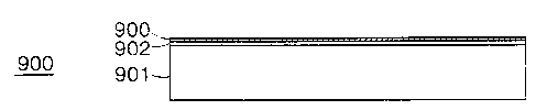
Fig. 9 illustrates a partial cross-sectional view
of a multilayer superconductor 900. Superconductor 900
includes an alloy substrate 901, a buffer layer 902 and a
superconductor material (e. g., oxide superconductor
material) layer 903.
Figure 9A illustrates a partial cross-sectional
view of a multilayer superconductor which includes two
buffer layers (904 and 905). A layer of superconductor
material (e.g., oxide superconductor material) 903 is
disposed on layer 905.
Figure 9B shows a partial cross-sectional view of
a multilayer superconductor which includes three or more
buffer layers (906, 907 and 908). A layer of
superconductor material (e. g., oxide superconductor
material) 903 is disposed on layer 908.
The preferred alloys can be prepared by several
methods. These methods produce an alloy of the first
metal and the second metal to which one or more oxide
formers can be added.
Referring to Figure 1, a block diagram illustrates
a melt process 100 for forming a preferred alloy article
with a biaxially, and preferably cube, textured surface.
CA 02365740 2001-09-27
WO 00/58044 PCT/US00/02435
- 14 -
The method includes selecting, weighing and mixing the
constituent metals of the alloy (Step 101).
The mixture is melted (Step 102) by various
processes known in the art, such as arc melting,
induction melting, melting in an electrical resistance
furnace, or a furnace heated by gas or coal. Melting
temperatures can be from about 900°C to about 1250°C. A
certain level of homogenization is achieved during the
melt process due to convection, mechanical stirring, or
stirring induced by the melting techniques such as in an
induction melter. The melting can optionally be
performed in air, or under a protective atmosphere such
as nitrogen, argon, helium or high vacuum.
Melting can be repeated a few times to further
increase homogenization (Step 103).
The melt is then cooled within the furnace and the
solidified melt is shaped, preferably into a bar. The
bar is reduced in diameter (e.g., by a factor of 1.3 to
5) by rolling, swaging, drawing or extrusion, and is then
heat treated to further homogenize the alloy (Step 104).
A further mechanical reduction in diameter, by
similar mechanical techniques follows, to a size where
the planar deformation process will commence (Step 105).
Before or at this stage, a heat treatment can be applied
to recrystallize the alloy and obtain a fine grain size
(e.g, from about 5 micrometers to about 70 micrometers or
from about 10 micrometers to about 40 micrometers) (also
Step 105). Alternatively, other methods can be utilized
to achieve a fine grain size, such as the rapid
solidification of the alloy after melting.
The alloy article is deformed in an axially
symmetric manner, such as, by extruding, swaging, drawing
or rod rolling to a smaller size, which can be round,
square, or rectangular (Step 106). Alternatively, the
melt can be cast and rolled directly into a plate shape.
CA 02365740 2001-09-27
WO 00/58044 PCT/US00/02435
- 15 -
The plate can be further homogenized with a suitable heat
treatment, rolled to a thinner size, and recrystallized
to induce a desired fine grain size.
The fine grained alloy article is deformed further
by various planar rolling methods known in the art (Step
107), to reduce the thickness of the stock (e. g., by from
about 85% to about 99.9°x).
A recrystallization anneal (Step 108) in a
protective atmosphere (e.g., high vacuum, low oxygen or
reducing atmosphere) at elevated temperature (e.g., at
temperatures from about 250°C to about less than about
95% of the melting temperature of the alloy, or from
about 400°C to about 1200°C) produces the desired
texture. The article is positioned to provide oxidation
resistance during subsequent uses, such as during
deposition of superconductor or buffer layers.
Alternatively, the article may be annealed (Step 109) to
form a protective epitaxial oxide layer.
Rolling processes suitable for use with methods of
the present invention as shown in Figs. 1 and 2, utilize
the following parameters. Rolling is typically performed
at room temperature, with a rolling speed of between
about 0.10 meters per minute and about 100 meters per
minute. The reduction schedule typically follows a
constant strain per pass, with reduction steps being set
at, for example, between about 5% and about 40% per pass.
The resulting tape can be lubricated during rolling, or
rolled without any lubricant. Bidirectional rolling is
preferred. The tapes can be rolled with various size
rolls, including large diameter rolls (e. g., about 3.5"
to about 8" or larger in diameter) or with small diameter
rolls (e. g., about 0.75" to about 2" in diameter) which
are preferably backed up by larger rolls, in a so-called
four-high arrangement. An alternative to the four-high
CA 02365740 2001-09-27
WO 00/58044 PCT/US00/02435
- 16 -
arrangement is the cluster rolling mill. A planetary
rolling mill can be used as well.
Referring to Figure 2, a block diagram illustrates
a process 200 for forming a biaxially textured alloy with
improved oxidation resistance, which uses a sheath and
core approach. A sheath is biaxially textured, which,
for example, can be a cube texture, while the core
provides a high concentration of oxide former needed to
provide the oxidation resistance during the subsequent
buffer layer and superconductor deposition processes.
For the sheath and core approach, a thick walled can
(Step 201) is made of stock of the first metal, the
second metal, or an alloy of the first and second metals,
and optionally one or more oxide formers. The thickness
of the wall is, for example, between about 5% and about
90% of the can outside radius. A core is made to fit
inside the can using a melt process or one of the
variations described below. (Step 202). The core
contains the alloy.
In one variation, known as the "rolled foil" or
"jelly roll" variation, as shown in Fig. 2A, individual
foils 220a-220b of the first metal, the second metal and
an oxide former or alloys thereof 220c, can be stacked
together and rolled into a bar 222, a so called "jelly
roll", which can be used as a core material or a wrapping
for a central core. Aluminum is a particularly useful
oxide former in making rolled foils, due to its
deformability. In Fig. 2B, the rolled foil bar 222 is
illustrated inside an outer layer of can 226 and is a
wrap material for a core 228. In Fig. 2C, the rolled
foil 222 is illustrated inside a can 226 process and is
the core for the can.
Referring to Figure 3, a block diagram illustrates
a process 300 for forming an alloy substrate with a
biaxially textured surface (or preferably cube textured
CA 02365740 2001-09-27
WO 00/58044 PCT/US00/02435
- 17 -
surface) and improved oxidation resistance, which uses a
powder metallurgy variant of the sheath and core
approach. This is one of the preferred embodiments of
the general sheath and core method illustrated in Figure
2. A sheath is worked into the desired biaxial texture
while a powder metallurgy core provides sufficient oxide
former to provide the oxidation resistance during buffer
layer and superconductor layer deposition. For this
approach 300, a thick walled can (step 301) is made of
stock of the first metal, the second metal, or an alloy
of the first and second metals, and optionally one or
more oxide formers as generally described in Step 301.
The thickness of the wall is between, for example,
about 5% and about 20% of the can outside diameter. The
can is filled with a mixture of elemental powders (step
302) or alternatively, pre-alloyed powders. The powder
mixture is poured into the can at tap-density (Step 302),
or is compacted into the can using a press with a.
compacting ram.
Each elemental or alloy powder should have the
ability to deform well when consolidated into a powder
mixture. The powders are then deformed to high areal
reductions in order to form the substrate. Many
elemental and alloyed fcc powders (i.e., face centered
cubic powders) have been found to be well suited. Some
hexagonal powders, such as Mg, are more difficult to
deform and are easier to incorporate in the as-alloyed
fcc solid solution, such as Cu-2 atomic % Mg. The same
is true for an element such as, for example, Ga which is
difficult to deform, and readily melts at ambient
temperature processing. An alloy such as Cu-5 atomic
Ga has been found to deform very well up to high areal
reductions; an atomized Cu-5 atomic % Ga powder has been
found to be the ideal way to incorporate this element in
the core of the substrate material. Other oxide formers,
CA 02365740 2001-09-27
WO 00/58044 PCT/US00/02435
- 18 -
like Y, are also difficult to deform, and require
deformation at elevated temperatures if an elemental
incorporation is desired.
Cores formed by a melt process, by a powder
metallurgy process, or by the rolled foil process of
Figs. 2A-2C, are placed inside the can and the assembly
is evacuated, sealed, and extruded, swaged, drawn, or
rolled to a smaller cross-sectional bar or tape (Step
203). This is processed further to a desired starting
size to enable for the planar rolling to commence (Step
204). The resulting bar, wire, tape, sheet or foil is
deformed in a planar manner such as rolling (Step 205),
to a reduction in thickness of between, for example,
about 85% and about 99.9%.
A partial cross-sectional view of the substrate
700 in this stage is shown in Fig. 7, with a powder
metallurgy core 702 inside of a can 701. Example seven
discusses the details of a process that uses a copper can
and a Cu+37 atomic % A1 PM core.
In Fig. 8 a partial cross-sectional view of a
substrate 800, in this stage of the process, shows a
core, such as a melt process core, 802 inside a sheath
801. A heat treatment (Step 206) follows in order to
develop biaxial texture on the surface of the sheath, and
to induce homogenization in the substrate. Temperatures
can range from, for example, about 250°C to as high as
95% of the melting temperature of the substrate. The
oxide former can diffuse towards the surface of the
substrate, but reach the surface after the biaxial
texture (or cube texture) has been developed on its
surface. The enrichment of the surface layer with oxide
formers tends not to adversely affect the quality of the
established cube texture. Upon diffusion, the oxide
former is positioned to provide oxidation resistance
CA 02365740 2001-09-27
WO 00/58044 PCT/US00/02435
- 19 -
during the subsequent buffer layers and superconductor
deposition processes.
Alternatively, the textured substrate can be
annealed (Step 207) in a gas flow with a low oxygen
partial pressure (e. g., between about 0.01 volume percent
and about 5 volume percent oxygen) to form an epitaxial
oxide layer which is part of the buffer layer, or can
serve as the buffer layer needed for the later
superconductor deposition process.
When using a copper sheath, a recrystallization
step at, for example, about 300°C remains possible before
commencing the rolling to refine the Cu grain size to,
for example, from about 5 micrometers to about 50
micrometers. The refined grain size is beneficial to
obtain a cube texture in the rolled and heat treated
tapes.
With small amounts of first oxide former (e. g.,
less than about 3 atomic percent) in the sheath, a same
or different oxide former can be added in larger
concentrations (e.g., about 3 atomic percent to about 25
atomic percent) to the core. Sheaths without oxide
formers may also be used. Pure elemental cores are also
possible for certain oxide formers, such as A1, Yb, or
Hf, Ce, Ti, Zr, or mixtures of these because of their
deformation ability. A high quality biaxial or cube
texture can be obtained on the surface of the alloy
article. The core can supply the oxide former, which
diffuses from the core to the surface of the substrate
after the texturing is completed, where it can form an
oxide (e. g., a native oxide).
Referring to Figure 4, a block diagram illustrates
a process 400 for forming an alloy article with a
biaxially textured surface or cube textured surface and
improved oxidation resistance, and which uses a variation
on the powder metallurgy embodiment or the rolled foil
CA 02365740 2001-09-27
WO 00/58044 PCT/IJS00/02435
- 20 -
embodiment of the sheath and core process. When
selecting the starting powders or foils (Step 401), a
powder or foil of the first metal, the second metal, or
an alloy of the first and second metals is chosen that
contains from about 0.2 weight percent to about 1 weight
percent oxygen. The presence of oxygen can be used to
assist in the internal oxidation of some of the oxide
formers. Additional powders or foils, such as an oxide
former which is easily deformable, or a pre-alloyed
powder or foil the first metal, is selected for a total
concentration, with the oxygen-containing powders or
foils, of 3 to 50 atomic % oxide former, and the balance
being the first metal (Step 402). The composite is to be
processed with the oxygen-containing starting powders or
foils. For example, a can of Cu is packed with a powder
mixture that includes 60 atomic % Cu-25 atomic % Ni-15
atomic % Al, all in elemental powder form. The Ni powder
contains 0.6 weight % oxygen, and the oxygen in the Cu
and A1 powder is negligible. The processing is similar
to the approach illustrated in Figure 200, except that
intermediate anneals are not recommended to avoid
premature hardening of the substrate material (Step 403).
During the final heat treatment (Step 404) at
temperatures which can range from 250°C to as high as 95%
of the melting temperature of the substrate, the oxygen
reacts to binds with a portion of the oxide former to
form an oxide dispersion strengthened alloy. Thus, in
the example, a small percentage of the A1 is used to bind
the oxygen in the Ni powder into A1203 to strengthen the
substrate. Any remaining A1 which is available enhances
the oxidation resistance of the substrate. These oxide
particles generally occupy 0.2 to 2 vol % of the core
material. For this type of strengthening, also known as
oxide dispersion strengthening, the result provides a
sufficiently large volume percentage of oxide particles
CA 02365740 2001-09-27
WO 00/58044 PCT/US00/02435
- 21 -
to significantly enhance both the room temperature and
high temperature strength of the substrate. Both types
of strength enhancement are important; room temperature
handling of the substrate, high temperature handling
during the various deposition processes, and then room
temperature handling of the final coated conductor in
subsequent cabling or winding operations.
Referring to Figure 5, a block diagram illustrates
a process 500 for forming an alloy with a biaxially
textured surface or cube textured surface and an improved
CTE (i.e., coefficient of thermal expansion) matches
among the substrate, the buffer layer, and the
superconductor layer. The mismatch between the CTE of
the primary substrate material and either the
superconducting layer or the buffer layer can be reduced
by incorporating into the alloy substrate another element
with a much lower CTE, such as Nb, Mo, Ta, V, Cr, Zr, Pd,
Sb, NbTi, an intermetallic such as NiAl or Ni3Al, or
mixtures thereof.
To assist in alloying these additional elements,
the CTE-reducing material is preferably included as a rod
embedded in the alloy. In one embodiment multiple CTE-
reducing rods may be used. Nb and NbTi are preferred
elements because they are quite ductile, and can be
deformed in a Cu matrix. The effect can be roughly
proportional to the volume of the Nb or NbTi, but at
elevated temperatures, when the Cu or CuNi begins
yielding at very low strains, the influence of the work
hardened Nb is even stronger as Nb does not recrystallize
at temperatures below 1100°C. In other words, only a
small amount of Nb (CTE: 7.5x10⁻⁶/°C) can be used in the
substrate to make it an effective CTE reducing agent.
Typically the rod of CTE reducing material occupies 5 to
vol% of the billet, with 10-20% being preferred. An
35 oxide former, such as A1 or Mg, is included in the alloy
CA 02365740 2001-09-27
WO 00/58044 PCT/US00/02435
- 22 -
that surrounds the CTE-reducing rod to provide oxidation
protection for the rod during the buffer layer and
superconductor layer deposition processes. This approach
to reduce the overall CTE of the substrate can be used in
any of the substrate-forming processes discussed above
(Step 501) or in the prior art processes for forming
superconducting substrates.
In a preferred embodiment, one or more rods of a
CTE-reducing material are placed in one or more bores in
the billet for process 100, or in the core of the
composite billet for processes 200, 300 or 400 (Step
502). The billet is processed into the final substrate
according to any of processes 100-400 (Step 503) with a
standard texturing heat treatment. The final substrate
includes one or more rods of CTE-reducing material which
reduce the overall CTE of the substrate, to preferably
about 10-15x10-6/°C, the exact value depending on the
composition and the volume % of the rods. However,
because the rods are located inside the substrate they do
not impair any biaxial texture which is developed on the
surface of the substrate by the process of the invention.
An illustration of a partial cross section of a substrate
produced by this process is shown in Fig. 10. In this
figure, the center includes a rod of CTE reducing
material 1004, such as Nb, surrounded by the substrate
material 1001. A buffer layer 1002 completely surrounds
the substrate material 1001 and has a superconducting
layer 1003 on at least one side. In one embodiment, the
rod can be coated with a thin layer, such as gold, which
can prevent a reaction between the rod and an alloy in
the core.
Referring to Figure 6, a block diagram illustrates
a process 600 for forming a biaxially textured or cube
textured alloy with improved surface smoothness. The
process may be used as a final step to smooth the
CA 02365740 2001-09-27
WO 00/58044 PCT/US00/02435
- 23 -
substrate before commencing the buffer layer deposition
or coating superconductor. The surface smoothness of the
substrate is a desirable aspect in the deposition of a
smooth, exclusively c-axis oriented superconducting film
(that is, with the c-axis normal to the substrate
surface). If the surface roughness exceeds 10-20 nm Ra
the current carrying capability of the superconductor
film can be strongly reduced. Rolling of substrate
materials as described can produce a very smooth surface,
well within the 10 nm roughness range. The heat
treatment to bring out the texture however can result in
grooves, which can increase the surface roughness.
Methods to remove these grooves, such as mechanical or
electro-polishing of the substrate, remove substrate
material as well, and can lead to a loss in dimensional
control.
In one preferred embodiment, a low reduction
rolling pass, following a recrystallization heat
treatment, restores the original surface smoothness,
while a low temperature stress anneal, at temperatures
below the recrystallization anneal, restores the high
quality biaxial texture to the surface of the substrate.
Any of the five processes 100-500 or a prior art
substrate forming process can be selected to make a
substrate with reduced surface grooving. The selected
process is first entirely completed, including the
texturing anneal (if any) (Step 601). The substrate is
subsequently rolled once or twice (Step 602) using a
reduction per pass of, for example, from about 5% to
about 300, with rolls having an extremely fine finish
(e. g., tungsten carbide with a 25-50 nm Ra surface
roughness or chromium-plated steel rolls with a 5 nm Ra
surface roughness). The substrate is then given a low
temperature stress anneal (Step 603), in a protective
environment which does not lead to a recrystallization.
CA 02365740 2001-09-27
WO 00/58044 PCT/US00/02435
- 24 -
A temperature range of from about 200°C to about 400°C is
typical. The resulting substrate has a very smooth
surface with a surface roughness of from about 5 Ra to
about 50 Ra and a well developed, undisturbed, and well-
s preserved biaxial texture.
Alloys that can be used as substrate for
superconductors, superconductor including such
substrates, and method of making these alloys, substrates
and superconductors are disclosed in commonly assigned
U.S. Patent Applications Serial No. , filed
on even date herewith and entitled "ALLOY MATERIALS",
08/943,047, filed October 1, 1997, and 08/942,038, filed
October 1, 1997.
Example 1
Copper metal of sufficient purity such as
Electrolytic Tough Pitch ("ETP") or Oxygen Free High
Conductivity ("OFHC") Cu, Ni metal with a purity of more
than 99%, Al metal with a purity of more than 98%, and Hf
and Ti metals with a purity of more than 98% are weighed
to obtain a Cu-16 atomic % Ni-0.5 atomic % A1-0.05 atomic
% Hf-0.05 atomic % Ti mixture. The weighed Cu, Ni, A1,
Hf and Ti are put in a suitable refractory crucible such
as (but not limited to) alumina or zirconia, and are
melted together. For a clean melt, an induction melter
can be used, in which the melting is done in vacuum or in
a protective atmosphere, but melting in air, and/or
melting using other heater types such as arc melting or
the use of resistance furnaces are possible. The alloy
is remelted two or three times to ensure additional
compositional homogeneity. The melting temperature is
1105°C. The cast is cleaned, and deformed by rolling,
swaging or extrusion to a smaller diameter with
sufficient size to allow subsequent deformation
processing. At this size, it is again homogenized by
holding the alloy at elevated temperatures for a few
CA 02365740 2001-09-27
WO 00/58044 PCT/US00/02435
- 25 -
hours to a few days, depending on temperature. Effective
temperatures should exceed 700°C. A preferable
combination is 12 hrs at 1000°C. The alloy bar is then
deformed by rod rolling, swaging, wire drawing or
extrusion to a smaller size, which is typically round or
rectangular in cross section, but can be oval or square
as well. All of these different cross sections have
been demonstrated to be equally effective for further
processing. The thinnest dimension typically varies
between lmm and l0mm. The alloy wire, rod, tape or strip
is then rolled to a thin tape or foil. The reduction in
thickness is larger than 80% and can be as high as 99.9%.
One example is the extrusion of a homogenized 30.5mm or
15.7mm diameter bar to a 3.8 mm x 2mm tape. The tape is
rolled to 37 micrometers, a reduction in thickness of
98.1%. Another example is the swaging of a bar to a
diameter of 6.2mm and subsequent rolling to a thickness
of 250 microns, a reduction in thickness by rolling of
96.0%. The rolling is performed with a conventional wire
flattening mill. A wide variety of rolling conditions
have been used successfully. For example, we have rolled
the CuNi based substrate materials at 5%, 100, 20% and
40% deformation per pass, using various lubrication
schemes, and at speeds as low as 0.1 meter per minute or
as fast as 100 meters per minute. In general, the lower
reductions per pass and lower processing speeds result in
somewhat improved textures.
The texturing anneal can be performed using a wide
range of temperatures, ranging from 250°C to close to the
melting temperature of the alloy (around 1105°C). The
higher temperatures require a shorter time and lead to
slightly better textures, but can increase surface
irregularities at the grain boundaries. This effect,
also known as thermal grooving, leads to depressions in
the surface at the grain boundaries due to surface
CA 02365740 2001-09-27
WO 00/58044 PCT/US00/02435
- 26 -
tension effects, and is less desirable for high quality
buffer layers and superconducting layers. Lower
temperature anneals have a much lower rate of thermal
grooving, but also a less well developed texture. The
temperature range of 850-1000°C, for a period of 1 to 24
hrs, and using a vacuum or protective atmosphere to avoid
oxidation of the substrate, are preferred conditions.
This process results in a substrate with a cube texture
and no substantial secondary textures, a FWHM value of 7-
9°.
The resulting thermal grooving is eliminated with
the following processing step. The texture annealed tape
is rolled once using very smooth rolls, typically with a
surface roughness of about 5 nm Ra, to a reduction of 5%
to 20%, with 10% being preferred. The substrate is then
stress annealed at low temperatures, 300°C being preferred
for the CuNi alloys, under protective atmosphere such as
a vacuum. This procedure does not adversely affect the
texture quality, or may improve it. It greatly enhances
the surface smoothness of the substrate material,
improving it to better than 5 nm Ra. The substrate is
then ready for the next step in the superconductor
manufacturing process, typically the application of a
buffer layer.
Example 2
Electrolytic Tough Pitch copper, nickel with a
purity grater than 99% aluminum with a purity greater
than 98o and hafnium and titanium with a purity greater
than 98% are weighed to obtain mixture containing 26.5
atomic % nickel, 0.5 atomic % aluminum, 0.05 atomic
titanium, and 0.05 atomic o hafnium with the balance
copper. The weighed metals are placed in an alumina
crucible. To insure a clean melt the charge is vacuum
induction melted at 1250° Celsius and a vacuum of 50
millitorr, and cooled to room temperature. The alloy is
CA 02365740 2001-09-27
WO 00/58044 PCT/US00/02435
_ 27 _
melted two more times to insure material homogeneity.
The melt is allowed to cool slowly, under vacuum, to
minimize voids due to shrinkage. The cast billet is 33
mm in diameter by 75 mm long. The billet is machined to
31.8 mm diameter to improve surface finish. The machined
billet is swaged to 16.8 mm diameter. After swaging the
billet is homogenized at 950° Celsius for 24 hours in a
protective argon 5% hydrogen reducing atmosphere. After
homogenization the billet is machined to 15.6 mm and
hydrostatically extruded to a tape with a 2 mm by 3.8 mm
cross section. The tape is then rolled with a constant
reduction of 0.127 mm per pass to 0.051 mm final
thickness, the reduction of the final pass being adjusted
as required to achieve the desired thickness. The
rolling is done on a four high wire flattening mill with
mm diameter work rolls and a speed of 3m per minute.
The finished tape is then annealed at 850° Celsius for 4
hours in a protective argon 5% hydrogen reducing
atmosphere. This process produces a tape having a cube
20 texture d surface with a FWHM of 12°, and no substantial
secondary texture.
Example 3
Electrolytic Tough Pitch copper, nickel with a
purity greater than 99% and aluminum with a purity of
25 greater than 98% are weighed to obtain a mixture
containing 37 atomic % nickel, 0.5 atomic o aluminum,
with the balance copper. The weighed metals are placed
in an alumina crucible. To insure a clean melt the
charge is vacuum induction melted at 1280° Celsius and a
vacuum of 50 millitorr, and cooled to room temperature.
The alloy is melted two more times to insure material
homogeneity. The melt is allowed to cool slowly, under
vacuum, to minimize voids due to shrinkage. The cast
billet is 33 mm in diameter by 75 mm long. The billet is
machined to 31.8 mm diameter to improve surface finish.
CA 02365740 2001-09-27
WO 00/58044 PCT/US00/02435
- 28 -
The machined billet is swaged to 16.8 mm diameter. After
swaging the billet is homogenized at 1000° Celsius for 24
hours in a protective argon 5% hydrogen reducing
atmosphere. After homogenization the billet is machined
to 15.6 mm and hydrostatically extruded to a tape with a
1.52 mm by 3.8 mm cross section. The tape is then rolled
with a constant reduction of 0.127 mm per pass to 0.061
mm final thickness, the reduction of the final pass being
adjusted to achieve the desired thickness. The rolling
is done on a four high wire flattening mill with 25 mm
diameter work rolls and a speed of 3m per minute. The
finished tape is then annealed at 850° Celsius for 4
hours in a argon 5% hydrogen atmosphere. This process
produces a tape and a cube textured surface with a FWHM
of 14°, and no substantial secondary texture. Figure 11
shows the (111) pole figure for this material.
Example 4
An alloy comprising Cu-1.2 atomic % Al is made
according to example 1. The alloy is made into a 16 mm
round bar, and is drilled along the axis to create a bore
in order to accommodate a 9.5 mm diameter Nb rod. This
CuAl+Nb composite billet is extruded to a 3.2 mm diameter
round exthudate, and subsequently drawn and rolled to
achieve a 97% reduction in thickness. An anneal at 850°C
yields a biaxially textured substrate. The Nb core does
not interfere with the surface texture of the substrate.
The CTE for this composite material is measured to be
13.4x10⁻⁶/°C at room temperature. In the extruded
material, the volume % of the Nb in the composite is
determined to be 37.6 volume %. This percentage yields a
calculated average CTE of 13.4x10⁻⁶/°C using the Rule of
Mixtures, confirming the measured value. The Rule of
Mixtures predicts that the CTE of a composite material is
the average of the CTE of its components (which are
17.0x10⁻⁶/°C for CuAl and 7.5x10⁻⁶/°C for Nb) , taking into
CA 02365740 2001-09-27
WO 00/58044 PCT/US00/02435
- 29 -
account their relative volume percentages. This
demonstrates that the CTE of a substrate can be carefully
adjusted to provide an improved CTE match with the buffer
layer and superconducting layer.
Example 5
Electrolytic Tough Pitch copper with a purity
greater than 99o and aluminum with a purity of greater
than 98% are weighed to obtain a mixture containing 9
atomic % aluminum, with the balance copper. The weighed
metals are placed in an alumina crucible. To insure a
clean melt the charge is vacuum induction melted at 1100°
Celsius and a vacuum of 50 millitorr, and cooled to room
temperature. The alloy is melted to more times to insure
material homogeneity. The melt is allowed to cool
slowly, under vacuum, to minimize voids due to shrinkage.
The cast billet is 33 mm in diameter by 75 mm long. The
billet is machined to 31.8 mm diameter to improve surface
finish. The machined billet is swaged to 16.8 mm
diameter. After swaging the billet is homogenized at
950° Celsius for 24 hours in a protective argon 5%
hydrogen reducing atmosphere. After homogenization the
billet is machined to 15.6 mm and hydrostatically
extruded to a tape with a 1.52 mm by 3.8 mm cross-
section. The tape is then rolled with a constant
reduction of 0.127 mm per pass to 0.061 mm final
thickness. the reduction of the final pass being
adjusted to achieve the desired thickness. The rolling
is done on a four high wire flattening mill with 25 mm
diameter work rolls and a speed of 3m per minute. The
finished tape is then annealed at 850° Celsius for 4
hours in a protective argon 5%hydrogen reducing
atmosphere. The finished substrate is heat treated at
830° Celsius using an oxidizing environment selected to
be typical of the environment utilized during one YBCO
deposition process, which is argon 1 vol oxygen gas,
CA 02365740 2001-09-27
WO 00/58044 PCT/US00/02435
- 30 -
followed by a 100% oxygen anneal at 400° Celsius. The
thin 40 micrometer thick substrate retains a biaxial
surface texture and is protected from the oxidizing
environment by the formation of a continuous native oxide
film.
Example 6
Electrolytic Tough Pitch copper with a purity
greater than 99% aluminum with a purity of greater than
98% are weighed to obtain a mixture containing 5 atomic
aluminum, with the balance copper. The weighed metals
are placed in an alumina crucible. To insure a clean
melt the charge is vacuum induction melted at 1080°
Celsius and a vacuum of 50 millitorr, and cooled to room
temperature. The allow is melted two more times to
insure material homogeneity. The melt is allowed to cool
slowly, under vacuum, to minimize voids due to shrinkage.
The cast billet is 33 mm in diameter by 75 mm long. The
billet is machined to 31.8 mm diameter to improve surface
finish. The machined billet is swaged to 16.8 mm
diameter. After swaging the billet is homogenized at
950° Celsius for 24 hours in a argon 5% hydrogen
atmosphere. After homogenization the billet is machined
to 15.6 mm and hydrostatically extruded to a tape with a
1.52 mm by 3.8 mm cross-section. The tape is then rolled
with a constant reduction of 0.127 mm per pass to 0.061
mm final thickness, the reduction of the final pass being
adjusted to achieve the desired thickness. The rolling
is done on a four high wire flattening mill with 25 mm
diameter work rolls and a speed of 3m per minute. The
finished tape is then annealed at 850° Celsius for 4
hours in an argon 5% hydrogen atmosphere. The finished
substrate is heat treated at 830° Celsius using an
oxidizing environment selected to be typical of the
environment utilized during one YBCO deposition process,
which is argon 1 volo oxygen gas, followed by a 100%
CA 02365740 2001-09-27
WO 00/58044 PCT/US00/02435
- 31 -
oxygen anneal at 400° Celsius. The thin 40 micrometer
thick substrate retains a biaxial surface texture and is
protected from the oxidizing environment by the formation
of a continuous native oxide film.
Example 7
A Cu-14.4 atomic % Al alloy is made using a
powder metallurgy sheath and core approach. A copper
powder made from electrolytic tough pitch copper, with a
particle size of 250 micrometers, and an aluminum powder
made by gas atomization, with a purity of 99%, and a
particle size of 220 micrometers, are mixed in a ratio of
63 atomic % Cu and 37 atomic % A1. The well-mixed Cu+A1
powder is compacted into an oxygen free high conductivity
copper billet which has an external diameter of 30.5 mm
and an internal diameter of 21.5 mm. The billet is
evacuated and extruded to a 9 mm bar. The bar is drawn
through round and rectangular drawing dies to a final
dimension of 2.4 mm x 3.6 mm. This rectangular product
is subsequently rolled to a tape of 65 microns thick
(97.3 % reduction). This tape is two-step annealed at
600°C and 800°C under protective atmosphere. This yields
a Cu 14.4 atomic % A1 substrate with a cube textured
surface, which has excelpd~eic~ation resistance.
A cube-textured copper-nickel-A1 alloy was
produced as follows. A 32 mm diameter copper (OFC) can
was loaded with a mixture of Cu, Ni and A1 pieces, and
the overall stoichiometry (including the weight of the
copper can) was further adjusted with Cu powder, to a
mixture of 51 at% Ni, 3.5 at% Al, 45.7 at% Cu. This can
was placed inside a 38 mm diameter thin-walled alumina
crucible and heated under vacuum using a induction
melter. After solidification the alloy was freed from
the crucible. The cast was remelted using a similar
crucible and the same induction melter, again under
vacuum. The cast alloy, which had a cylindrical shape,
CA 02365740 2001-09-27
WO 00/58044 PCT/US00/02435
- 32 -
was machined to a diameter of 31 mm and swaged to a 18 mm
diameter bar. This bar was homogenized at 950°C for 16
hrs. It was machined to a 16 mm diameter billet,
suitable for hydrostatic extrusion at elevated
temperatures. It was extruded to a 6.4 mm diameter wire.
This wire was annealed for one hour at 600°C. It was
subsequently drawn through drawing dies with a square
cross sections, measuring 5.8 mm x 5.8 mm and 5.3 mm x
5.3 mm. This square wire was subsequently rolled using a
reversible direction rolling technique, a two high
rolling mill down to a thickness of lmm, and a four-high
rolling mill down to a thickness of 0.015mm or less. A
rolling speed of 6 m/min was used. Subsequently, it was
heat treated at a 850°C for 2 hrs under a 95% argon with
5% hydrogen gas mixture, or vacuum.
This foil had a single bi-axial (100) (001] cube
texture as by a 200 reflection in the theta-two theta X-
ray diffractogram. No second components were visible.
The (111) pole figure is shown in Fig. 12. Only a cube
texture, with a FWHM value of 9° is observed.
The annealed substrate had a yield stress (at 0.2%
strain) of 26.5 ksi at room temperature.
This substrate was polished after anneal to a
surface roughness of Ra=5nm. Polishing did not affect
the surface texture. The substrate was put in a vacuum
chamber, which is evacuated to 10-6 torr. The sample was
heated to 800°C and provided with an epitaxial yttria-
stabilized zirconia buffer layer, which had a layer
thickness of 0.6 micrometer, using a Pulsed Laser
Deposition method. Subsequently a 1 micrometer thick
epitaxial YBa2Cu30~_X layer was deposited on top of the
buffer layer. The YBazCu30~_X layer was superconducting,
and demonstrated a superconducting critical current
density of 160,000 A/cm2 at 75K, in the absence of a
magnetic field other than the small magnetic field
CA 02365740 2001-09-27
WO 00/58044 PCT/US00/02435
- 33 -
created by the current in t'~~~ tape itself (the so-called
self field).
Example 9
An ingot was vacuum cast having the following
composition: 47.4 at% Ni, 2.2 at% Al, and 50.4 ato Cu.
The ingot had a length of 15", and a diameter of
approximately 3". The ingot was machined to a 2.5" round
billet with a length of 8". This billet was heated to
1000°C in a flowing argon atmosphere, and subsequently
extruded in a 300 ton ram-type extrusion press to a 1'°
diameter bar. The bar was cleaned and homogenized at
1000°C for 16 hrs. It was swaged to 0.75" diameter using
a four-die swaging machine. The bar was stress relieved
at 600°C and rolled using a 2H rolling mill to a
0.3"x0.77" strip without using lubricant. The strip was
heat treated at 650°C, and polished. It was rolled using
5% reduction per pass to 0.1" thickness in a 2H rolling
mill using a suitable lubricant, and mirror polished
steel rods. It was rolled to 0.008" thickness using a 5%
or 10% or 20% reduction per pass. Higher reductions per
pass were favored as it enhances the production speed.
The 0.008" thick foil was heat treated at 1000°C for 45
minutes. This foil had a cube textured surface with a 9°
FWHM. It had a grain size of 50-100 micrometer, with no
evidence of abnormal grain growth.
Example 10
The production of substrates with a composition of
Cu with more than 0.5 at% Al by rolling and annealing can
lead to mixed textures (e. g. a so-called brass textures).
To make cube textured substrates with a composition such
as Cu-3.5 at% Al or Cu-9 at% A1 copper cans were filled
with a mixture of copper and aluminum.
The mixture was formed by using copper and
aluminum powders. These powders were co-extruded in the
copper can to a rod, which was then rolled and texture
CA 02365740 2001-09-27
WO 00/58044 PCT/US00/02435
- 34 -
annealed. The copper sheath rapidly formed a cube
texture while with prolonged time the aluminum diffused
to the cube-textured surface and created a Cu-3.5 or 9
at% Al substrate with a sharp cube texture.
Two billets were made for ram type extrusions in a
300 ton extrusion press. The cans were eight inches
long, consisted of pure copper. Cu and A1 powders were
mixed using two types of mixtures. In the first mixture,
the composition was 95 at% Cu-5 at%A1. In the second
mixture, the composition is 86 at% Cu-14 at% Al. After
compaction, extrusion, rolling and annealing the aluminum
diffused into the sheath, and a homogeneous substrate
remained, with an overall compositions of Cu-3.5 at% Al
and Cu-9 at% A1. Powders were carefully mixed and poured
in six or seven steps into the cans. After each fill the
mixture was compacted at 7 ksi, yielding about 750
packing density. This was sufficiently dense to prevent
the collapse of the wall during extrusion, but
sufficiently loose to allow fast outgassing during
evacuation. The cans were capped with a Cu cap. The Cu
caps had a grove in the side to facilitate outgassing.
The billets were put in the chamber of an E-beam welder
and evacuated overnight. The caps were then welded using
a welding depth of approximately 1/4". The cans cooled
in the chamber and are subsequently transported to the
extrusion facility. During the upset stroke the billet
compacted quite homogeneously to close to 100% density
before actual extrusion starts.
The billets were pre-heated at 250°C, and extruded
to a 1" round bar. The extrudates were water-quenched
after extrusion. The extrudates were swaged with a four-
die swager to 0.75" diameter. These were then rolled
using a 2H rolling mill to a 0.008" thick substrate. No
stress anneals were used or needed. The rolling mill had
a set of 4" diameter steel rolls, polished to a mirror
CA 02365740 2001-09-27
WO 00/58044 PCT/US00/02435
- 35 -
finish. This resulted in a surface roughness value Ra of
about 10 nm at the substrate as measured with a Zygo
light interference microscope. Figs. 13a-c show, at
varying magnification (4x, 40x and 175x, respectively) a
perpendicular cross-section of the Cu-9 at% A1 tape
during the rolling process, at a thickness of 0.050".
The tapes were about 0.88" wide. The powder cores, still
elemental Cu+Al, were well-defined, as were the
individual Cu/Al interfaces of the particles inside the
cores as can be seen in Figs. 13b and 13c.
The PM tapes were annealed at 800-900°C, using
either a single heat treatment at a temperature equal to,
or exceeding later processing conditions anticipated for
buffer and YBCO deposition or a stepped heat treatment,
to avoid texture formation when the Al is still liquid.
The stepped heat treatments gave better results with
regards to texture. Note that at 600-900°C the Cu sheath
can give a cube texture in a very short time, in the
order of a few minutes, and that the subsequent time is
intended to diffuse the A1 into the cube textured sheath.
Six examples of heat treatments for the Cu/Cu+A1 PM tapes
were:
1. 400°C-44h+600°C-12h 2. 600°C-12h
3. 600°C-12h+800°C-4h 4. 400°C-44h+600°C-
12h+800°C-4h
5. 600°C-12h+900°C-lh 6. 400°C-44h+600°C-
12h+900°C-lh
Fig. 14 shows the XRD pattern of the Cu-Sat%A1
sample, annealed at 400°C-44h+600°C-12h+900°C-lh. It
shows only the (200) peak, with no other peaks observable
at this intensity (ImaX=600, 000) . Fig. 15 shows the
magnified patterns of the six anneal conditions for Cu-
9at%Al listed above, where: the bottom curve corresponds
to heat treatment 1; the second curve from the bottom to
CA 02365740 2001-09-27
WO 00/58044 PCT/LJS00/02435
- 36 -
heat treatment 2; the third curve from the bottom to heat
treatment 3; the third curve from the top to heat
treatment 4; the second curve from the top to heat
treatment 5; and the top curve to heat treatment 6. I,n~X
is 12,000, indicating a 50x magnified intensity. Small
(111) and other peaks are observable for some of the
anneals, while the stepped anneal shows the cleanest
pattern. Fig. 16 shows the (111) pole figure of the tape
annealed at 400°C-44h+600°C-12h+900°C-lh. The (111)
poles are very sharp, with a FWHM of about 5-6°. The
(200) pole figure is equally sharp, and again very
symmetric in all directions. Fig. 17 shows a magnified
(111) pole figure, where the intensity is magnified by
about 280x. This shows a few grains with random
orientations. Based on integrated X-ray intensities
within the (111) pole figure, the cube texture is about
99.10, with about 0.4% random grains, and no annealing
twins.
Fig. 18 shows the $-2~ X-ray diffraction scans for
the six anneal conditions of Cu-3.5at%A1 listed above,
where only the (200) peak is observable. The pole figure
looks very similar to that of the Cu-4%Al sample, with
the same low FWHM value.
What is claimed is: