Note : Les descriptions sont présentées dans la langue officielle dans laquelle elles ont été soumises.
CA 02366200 2001-09-12
WO 00/55663 PCT/US00/06868
OPTICAL NETWORKING ASSEMBLY
STATEMENT REGARDING RELATED APPLICATIONS
This application is related to U.S. Patent Application Serial No. 09/267,258
entitled, "Method and Apparatus for Filtering an Optical Fiber," and claims
the benefit
of priority to U.S. Provisional Application No. 60/124,424 entitled, "Optical
Networking Assembly," filed March 15, 1999.
TECHNICAL FIELD
This invention relates generally to the manipulation of light carried by
optical
fibers. More particularly, the present invention relates to filtering light
and propagating
reflected light along optical paths of a planar lightguide circuit.
BACKGROUND OF THE INVENTION
In recent years, the use of optical fibers has become increasingly widespread
in
a variety of applications. Optical fibers have been found to be especially
useful for
many industries such as telecommunications, computer-based communications, and
other like applications.
To maximize efficiency of optical waveguides, multiple information channels
can be multiplexed into a single optical beam. In other words, multiple
channels of
information can propagate along an optical waveguide as a single beam of light
energy.
In order to form the multiplexed optical signal or to demultiplex the optical
signal,
optical filters are typically employed to separate light energy of a first
wavelength from
light energy having different wavelengths. To maximize optical filter
efficiency, light
energy can be collimated such that rays of light forming an optical beam
travel in a
manner parallel with one another. Such a collimation of light energy enables
individual
rays to strike an optical filter at a desired angle. Without collimating light
energy,
individual rays of light could strike an optical filter at undesirable angles
which reduces
optical filter efficiency.
For example, in the conventional art as illustrated in FIG. l, an expanded
beam
optics system 10 can be used to separate channels of information of a single
optical
1
SUBSTITUTE SHEET (RULE 26)
CA 02366200 2001-09-12
WO 00/55663 PCT/US00/06868
beam 20 that propagates along an optical waveguide 15. Each channel of the
single
optical beam 20 can have a different wavelength. For example, the single beam
20 as
illustrated in FIG. 1 can include separate information channels that are
carried by a first
optical beam having a wavelength of lambda sub one (A, ) and a second optical
beam
having a wavelength of lambda sub two (AZ).
The expanded beam optics system 10 can employ a lens 30 to collimate the
beams of optical energy forming the single optical beam 20. The lens 30 is
necessary
hardware for the conventional system since whenever optical energy leaves one
medium and enters into another medium the optical energy refracts or diverges
because
of the changes in the indices of refraction of the different materials. In
addition to the
lens 30, the expanded beam optics system 10 also uses free space 40 between an
optical
filter 50 and the lens 30. The free space 40 may be open space or it may
include
another medium such as a glass block (not shown).
In FIG. l, a few of the optical beams 25 that form the single beam 20 are
illustrated in order to demonstrate that the individual optical beams 25 are
substantially
parallel with one another when exiting the lens 30. When the individual
optical beams
strike the optical filter 50, only optical beams of a predetermined wavelength
are
permitted to pass through the optical filter 50. In the example illustrated in
FIG. 1, the
optical filter is designed to pass only optical beams having a wavelength of
lambda one
20 (A~). The individual optical beams 25 having a wavelength of lambda one
(AI) pass
through the optical filter 50 and through a glass plate 60 that supports the
optical filter
50. The filtered optical beam 70 exits the glass plate 60. The light reflected
off of
optical filter 50 has optical beams that have wavelengths other than lambda
one (A1),
such as lambda two (AZ).
25 One of the drawbacks of the conventional art is that with such a
traditional
optics systems 10 larger mechanical configurations are required. In other
words, the
lens 30 is typically large and bulky relative to the size of the optical
waveguide 15.
Furthermore, the amount of collimation for light energy with a lens 30 can be
directly
related to the cross sectional area of the optical beam. Expanded beam optics
systems
10 require precision alignment and mounting of the optical devices relative to
each
other. In other words, the optical waveguide 15 must be in precise alignment
with the
lens 30 to promote optical efficiency. Similarly, the lens 30 must be in
precise optical
2
SUBSTITUTE SHEET (RULE 26)
CA 02366200 2001-09-12
WO 00/55663 PCT/US00/06868
alignment with the optical filter 50 in order to also promote optical
efficiency. Such
configurations are not cost efficient for mass production. Additionally, much
optical
signal loss can occur between the waveguide-lens interface and the lens-free
space
interface.
Accordingly, a need in the art exists for separating optical energy into
separate
optical beams of different wavelengths with a higher efficiency. There is a
further need
in the art for a system for separating optical energy that can optimize the
transfer of
single mode optical energy propagation between an optical waveguide and a
filtering
device. An additional need in the art exists for a system that can tolerate a
certain
amount of misalignment between optical hardware without introducing
substantial
optical losses. Another need exists in the art for a system separating optical
energy that
can be easily manufactured and scaleable smaller sizes compared to traditional
expanded beam optics that require a substantial amount of hardware. Another
need
exists in the art for a system for separating optical energy without the use
of lenses.
SUMMARY OF THE INVENTION
The present invention solves the problems of expanded beam optics systems by
providing an optical network assembly that includes a planar lightguide
circuit (PLC)
and a filtering device. A PLC can have at least two optical paths for
propagating
optical energy. The PLC can be designed to channel optical energy to the
filtering
device in order to separate the optical energy into at least two beams, where
a first
beam can contain a first information channel and a second beam can contain a
second
information channel. The filtering device can be attached directly to the PLC
or it can
be attached directly to an optical waveguide that is also connected to the
PLC. This
direct attachment can be accomplished by building up the filtering device on
the PLC
or on the optical waveguide with a thin film deposition process. The optical
waveguide
can be a flexible optical fiber that is part of a communications network. The
optical
waveguide can either feed optical energy to or propagate optical energy away
from the
PLC. Multiple optical waveguides can be attached to a PLC to feed optical
energy into
and away from the PLC.
Each optical path of a PLC can be made of a transparent core of relatively
high
refractive index, light-conducting material while the planar material
surrounding an
3
SUBSTITUTE SHEET (RULE 26)
CA 02366200 2001-09-12
WO 00/55663 PCT/US00/06868
optical path can be made of a medium having a lower refractive index. The
optical
paths can be made of silica, plastic, glass, or low-to-no expansion optical
material such
as ZERODUR glass. Each of the optical waveguides can be made of materials
similar
to a PLC. Both the optical waveguides and PLCs can be designed to propagate
single
modes of optical energy such that the optical energy travels as a single
wavefront in
order to reduce attenuation and other undesirable effects while increasing
bandwidth
and transmission properties such as increases in traveled distances.
A PLC or a filtering device (or both) can optimize transfer of single mode
optical energy propagation (referred to as modal transfer) between an optical
waveguide and the PLC. The PLC and filtering device can be designed to
minimize
modal disruption (such as changes in E-Field geometry) of optical energy that
can
occur during the modal transfer of the optical energy between an optical
waveguide and
the PLC. A PLC can minimize modal disruption that occurs within an interface
or
junction between the PLC and another light carrying device by facilitating
efficient
alignment between the PLC and the other light carrying device.
In other words, a PLC's geometry permits rapid and efficient allignment
between a PLC and another light carrying device such as an optical waveguide.
A PLC
in combination with another light carrying device can tolerate a certain
amount of
misalignment relative to each other without introducing substantial optical
losses. This
tolerance of misalignment can also increase manufacturability of an optical
system that
includes a PLC since dimensioning of both a PLC and other light carrying
device can
be relaxed.
Furthermore, a PLC can permit the use of passive alignment techniques that can
reduce time as well as expense compared to conventional active alignment
techniques
that require signal propagation measurements. That is, with passive alignment,
signal
propagation testing can be substantially eliminated. Additionally, PLCs can be
scaled
to smaller sizes compared to traditional expanded beam optics that require
additional
hardware such as lenses. PLCs can interact with filtering devices without the
use of
lenses that are typically required in traditional optics to collimate optical
energy.
Similar to a PLC, a filtering device in combination with a PLC can optimize
the
modal transfer between a PLC and another light carrying device. One way to
optimize
modal transfer between a light carrying device and a PLC is to deposit the
filtering
4
SUBSTITUTE SHEET (RULE 26)
CA 02366200 2001-09-12
WO 00/55663 PCT/US00/06868
device directly on the PLC itself or the light carrying device that can be
connected to
the PLC. Another way to optimize modal transfer between a light carrying
device and
a PLC is to reduce a thickness of the filtering device such that optical
energy can be
transferred to or away from a PLC in the near field. In other words, by
reducing the
thickness of a filtering device, divergence of optical energy propagating
through the
filtering device can be reduced or become negligible because the interface
between the
PLC and light carrying device is substantially small such that optical energy
is
essentially channeled in a waveguide between the light carrying device and
PLC.
Another way to optimize the modal transfer of optical energy between a light
carrying device and a PLC is to provide modal adaptations such as changes in
geometry
in the vicinity of the PLC-light carrying device junction in order to shape
the actual
mode fields of optical energy. For example, the cross sectional geometry of
the either
the PLC or light carrying device or both can be adjusted to match each other
such that
the mode field propagated by the PLC matches the mode field propagated by the
light
carrying device.
A filtering device can optimize modal transfer between a light carrying device
and a PLC by increasing the packing density of the filtering device such that
the
filtering device approaches a bulk density. In other words, an increased
packing
density of a filtering device can substantially reduce or eliminate voids
within the
filtering device that interfere with the propagation of optical energy. Such
voids can
trap light reflecting or light disturbing materials such as water vapor.
The PLC and filtering device can form building blocks for more complex
optical networks or network architectures. In one aspect of the present
invention, a
PLC and filtering device combination can form a drop or add configuration
where one
channel of information propagating within a multichannel or multiplexed
optical beam
can be either dropped from or added to the multichannel or multiplexed beam.
In
another aspect, the PLC and filtering device combination can form a single
channel
drop-add configuration where one channel can be dropped from a first
multichannel
optical beam and then added to a second multichannel optical beam.
In yet another aspect, optical paths within a PLC can be non-linear or curved
in
order to provide control over an angle of incidence of an optical beam
striking the
filtering device to minimize obliqueness. The PLC and filtering device
combination
5
SUBSTITUTE SHEET (RULE 26)
CA 02366200 2001-09-12
WO 00/55663 PCT/US00/06868
can form a waveguide-constrained cascade where the PLC can include multiple
optical
paths that lead to a plurality of filtering devices. Such waveguide-
constrained cascades
can either multiplex or demultiplex optical energy that propagates through
light
carrying devices. The PLC and filtering device combination can multiplex
separate
optical beams having individual channels into a single optical beam or
demultiplex a
single optical beam into separate optical beams with distinct or different
channels.
In another aspect, the PLC and filtering device combination can include
multiple mirrors coupled to the PLC that re-direct optical energy onto a
plurality of
filtering devices. This can refocus optical energy in order to reduce any
optical beam
divergence as the optical energy reflects off of a filtering device.
Alternatively, the
PLC and filtering device combination can form a daisy-chained path waveguide
that
can optimize positioning or allignment of the optical paths of a PLC with a
plurality of
filtering devices.
In a further aspect, the PLC and filtering device combination can form a
remotely configurable drop-add plus optical cross connect network. The PLC and
filtering device combination can further include an activating or diverting
element such
as a moving mirror that diverts a channel signal out of an optical circuit
while
introducing a new signal content along the same channel into the optical
circuit. This
embodiment can function as an optical switch.
For an additional aspect the PLC and filtering device combination form a part
of
an amplification or gain flattening architecture. Gain flattening elements can
be
inserted into light paths outside of the PLC and filtering device combination
to
discretely attenuate channels which in turn flattens the gain of an optical
signal over an
extended spectral range.
Similar to how the PLC and filtering device combination can form building
blocks for optical network architectures, the multiplex, demultiplex, and the
optical
drop-add inventive concepts can form building blocks for even larger network
architectures. These larger network architectures can include a multiplex-
demultiplex
configuration and an optical drop-add configuration. In a multiplex-
demultiplex
configuration, multiple beams that each carry a unique information channel can
be
combined or multiplexed into a single optical beam. This single optical beam
can then
be propagated along a light carrying device to another PLC and filtering
device
6
SUBSTtTUTE SHEET (RULE 26)
CA 02366200 2001-09-12
WO 00/55663 PCT/US00/06868
combination that can then demultiplex the single optical beam into multiple
optical
beams. In the optical drop-add configuration, multiple channels can be
multiplexed
into a single optical beam and a few channels can be dropped or added or both
at a
point between two PLC-filtering device combinations that multiplex and
demultiplex
the single optical beam.
The PLC and filtering device combination, in addition to the multiplex-
demultiplex configuration and optical drop-add configuration, can form an
optical
cross-connect configuration that permits the sharing of optical channels
between at least
two separate optical networks. The PLC can be formed with a single segment of
optical material suitable for an optical waveguide. A sharp bend of an
appropriate
angle can be introduced into the single segment of optical material so that
the PLC and
the optical waveguide form an integral unit.
A PLC can be integrated into a bulk matrix. This structure can be formed by
utilizing polymer molding techniques such as insert injection molding or by
planar
waveguide fabrication.
The PLC and filtering device combination can further optimize modal transfer
of optical energy by manipulating the shape of the optical paths disposed
within a PLC.
In other words, an optical path of a PLC can be shaped in such a way as to
minimize
the divergence of optical energy as the optical energy passes through the
filtering
device. An optical path within a PLC can be tapered so that optical energy is
projected
optimally through the filtering device and into a fiber core of an optical
waveguide.
The shaping of optical paths within a PLC can reduce losses that can occur
when
optical energy propagates through the filtering device.
The PLC and filtering device combination can be part of mounting structures
that facilitate the precise alignment of light carrying devices such as
optical waveguides
with each PLC and filtering device. These mounting structures can include
blocks
comprising cavities having a shape similar to a respective PLC. Other mounting
structures can include V-groove based assemblies that are designed to align
optical
waveguides by supporting the outer cladding of optical waveguides with a
respective
V-groove. The V-grooves can be made at appropriate angles relative to one
another as
dictated by the number of optical wage guides to be coupled and the type of
PLC and
filtering device being employed.
7
SUBSTITUTE SHEET (RULE 26)
CA 02366200 2001-09-12
WO 00/55663 PCT/US00/06868
That the present invention improves over the drawbacks of the conventional art
and accomplishes the objects of the invention will become apparent from the
detailed
description of the illustrative embodiments to follow.
BRIEF DESCRIPTION OF THE DRAWINGS
FIG. 1 illustrates an expanded beam optics system of the conventional art for
the separation of optical energy into optical beams of different wavelengths.
FIG. 2 is a diagram that illustrates a single-channel drop or add
configuration
according to an exemplary embodiment of the present invention.
FIG. 3 is a diagram that illustrates a single-channel drop-add configuration
according to an alternate exemplary embodiment of the present invention.
FIG. 4 is a diagram that illustrates a straight-line path single-channel drop-
add
configuration according to an alternate exemplary embodiment of the present
invention.
FIG. 5 is a diagram that illustrates a serpentine path single-channel drop-add
configuration according to an alternate exemplary embodiment of the present
invention.
FIG. 6 is a diagram that illustrates an eight-channel demultiplex or multiplex
configuration according to an alternate exemplary embodiment of the present
invention.
FIG. 7 is a diagram that illustrates a four-channel drop-add configuration
according to an alternate exemplary embodiment of the present invention.
FIG. 8 is a diagram that illustrates a four-channel drop configuration that
employs concave mirrors according to an alternate exemplary embodiment of the
present invention.
FIG. 9 is a diagram that illustrates a daisy chained path configuration
according
to an alternate exemplary embodiment of the present invention.
FIG. 10 is a diagram that illustrates a dynamically and remotely configurable
drop-add plus optical cross-connect format configuration according to an
alternate
exemplary embodiment of the present invention.
FIG. 11 is a diagram that illustrates an element in an optical path such that
existing optical channel content of a light circuit can be diverted while new
channel
content can be introduced to the light circuit in accordance with the
embodiment
illustrated in FIG. 10.
8
SUBSTITUTE SHEET (RULE 26)
CA 02366200 2001-09-12
WO 00/55663 PCT/US00/06868
FIG. 12 is a diagram that illustrates an element out of path such that
existing
optical channel content of a light circuit can be uninterrupted and alternate
channel
content can continue on its path according to the embodiment illustrated in
FIG. 10.
FIG. 13 is a diagram that illustrates an optical architecture for optical gain
flattening and selective spectral amplification according to an alternate
exemplary
embodiment of the present invention.
FIG. 14 illustrates a configuration to introduce pump light according to an
alternate exemplary embodiment of the present invention.
FIG. 15 is a diagram that illustrates a multiplex-demultiplex configuration
according to an alternate exemplary embodiment of the present invention.
FIG. 16 is a diagram that illustrates an optical drop-add configuration for
two
networks according to an alternate exemplary embodiment of the present
invention.
FIG. 17 is a diagram that illustrates an optical cross-connect configuration
that
permits communication between multiple networks according to an alternate
exemplary
embodiment of the present invention.
FIG. 18 is a diagram that illustrates a single-channel drop or add
configuration
that includes a shaped planar lightguide circuit according to an alternate
exemplary
embodiment of the present invention.
FIG. 19 is a diagram that illustrates a planar lightguide circuit integrated
into a
bulk matrix according to an alternative exemplary embodiment of the present
invention.
FIG. 20 is a diagram that illustrates a planar lightguide circuit with shaped
optical paths according to an alternate exemplary embodiment of the present
invention.
FIG. 21 is a diagram that illustrates a mounting structure for optical
waveguides
and a planar lightguide circuit.
FIG. 22 is a diagram that illustrates a top view of a V-groove-based mounting
structure according to an alternate exemplary embodiment of the present
invention.
FIG. 23 is a diagram that illustrates a mounting structure for optical
waveguides
according to an alternate exemplary embodiment of the present invention.
FIG. 24 is a diagram that illustrates a optical waveguide that includes a thin-
film
interference filter and a fiber Bragg grating according to an alternate
exemplary
embodiment of the present invention.
9
SUBSTITUTE SHEET (RULE 26)
CA 02366200 2001-09-12
WO 00/55663 PCT/LTS00/06868
DETAILED DESCRIPTION OF EXEMPLARY EMBODIMENTS
To understand the operation and design of planar lightguide circuits (PLCs), a
review of fiber optics in general can be beneficial to the reading audience.
The term
"optical fiber" is used herein to refer generally to any optical waveguide or
structure
having the ability to transmit the flow of radiant energy along a path
parallel to its axis
and to contain the energy within or adjacent to its surface. "Step index,"
"gradient
index," and "single mode" fibers are subcategories within the optical fiber
designation.
The term "multimode" optical fiber refers to an optical waveguide that will
allow more
than one bound mode to propagate.
Step index fibers include a transparent cylindrical core of relatively high
refractive index light-conducting material. Typical core materials include
silica, plastic,
and glass. The core is cylindrically surrounded by a medium having a lower
refractive
index. Typically, this medium is a relatively thin cladding, which is an
intimately
bound layer surrounding the core. The cladding may be a different material
than the
core, or it may be a similar material that has been doped in order to reduce
its refractive
index. The core may also be unclad whereby the ambient medium, often air, is
of lower
refractive index and acts in the capacity of the cladding. The cladding is
usually
surrounded by one or more coatings, buffers, and/or jackets that primarily
serve
protective roles.
An arbitrarily oriented ray within the core of a step index fiber travels
until it
intersects the core boundary at the cladding and interacts in accordance with
its angle of
incidence. Generally, rays angularly oriented close to parallel with the
fibers axis are
efficiently reflected at the core boundary. Within certain angular
limitations, the ray is
oriented to undergo total internal reflection at the core interface. These
angular
limitations are a function of the refractive indices of the core and the
cladding. The
limits determine the angular bounds within which the fiber can propagate
light. Thus,
sustained propagation occurs via repeated total internal reflection within the
fiber core.
If the arbitrary ray is oriented beyond the fiber's limits for total internal
reflection, then
only a fraction of its intensity is internally reflected. The reduced
intensity ray is further
attenuated as it undergoes subsequent core boundary interactions. The ratio of
light
energy that is internally reflected to the energy that escapes varies
according to the
angle. If the ray is oriented normal to the core boundary, then all of its
intensity is lost.
SUBSTITUTE SHEET (RULE 26)
CA 02366200 2001-09-12
WO 00/55663 PCT/US00/06868
As the angle of an improperly oriented ray approaches the acceptance limits
for total
internal reflection, the relative intensity of the reflected ray increases.
Thus, for rays
with angle orientation close to, but outside of, the limits for total internal
reflection,
multiple reflections can occur prior to significant power loss.
If the arbitrarily oriented ray within the fiber core has sufficient power and
orientation, then it sustains power and eventually reaches the fiber end face.
It interacts
with the end face boundary in accordance with the laws of reflection and
refraction. As
the ray crosses the end face boundary between the fiber's core and the
surrounding
medium, it is refracted. The refractive effect is a function of the refractive
index of the
core, the refractive index of the surrounding medium, and the orientation of
the ray
relative to the fiber end face surface. The factor of ray orientation is based
upon its
angle relative to a surface normal taken at the point where the ray intersects
with the
end face surface boundary. Angular orientation of rays outside the fiber end
face and
propagating rays within the fiber core are distinctly correlated. A
correlation exists
between individual and collective external and internal rays.
The previous discussion centered on rays internally propagating and exiting
the
fiber. An analogous situation exists for rays outside the optical fiber
entering into the
fiber core. The correlating development is readily drawn by those skilled in
the art. For
a fiber utilized for single-direction flow of light, light is typically
injected into the fiber
at one end and exits the fiber at the opposite end. However, fibers can also
be utilized in
a bidirectional configuration. In this configuration, light purposely enters
and exits from
a single end of the fiber.
As light propagates within the fiber core, it tends to become mixed or
randomly
oriented over distance. Even highly directional sources, such as lasers,
become mixed
or scrambled over distance following input into a long optical fiber. In this
mixing
process, the fiber's modes are filled and all source characteristics, or so-
called launch
conditions, are lost. The mixing process can be accomplished in shorter fibers
by tightly
coiling the fiber, inducing micro-bends, or otherwise stressing the fiber.
Similarly, for
very short fiber lengths, launch characteristics are retained. Also, for very
short lengths
of fiber, light can be transmitted beyond the normal limits for propagation
dictated by
the angular limits for total internal reflection. This property is due to the
reduced
number of reflections, which accumulate minimal attenuation. A fiber's ability
to
11
SUBSTITUTE SHEET (RULE 26)
CA 02366200 2001-09-12
WO 00/55663 PCT/US00/06868
sustain transmission beyond the normal limits for total internal reflection
can be
enhanced by the application of internally reflective coatings applied to the
fiber's outer
cylindrical surface. This coating can be applied to either the fiber's core or
the cladding.
It should be noted that, for long fibers, propagation cannot be totally
reliant on
reflective coatings. In contrast to total internal reflection, even the best
reflective
coatings offer less than 100 percent reflectivity. Losses associated with
repeated
reflections at less than 100 percent efficiency quickly accumulate resulting
in severe
attenuation. Vast numbers of reflections occur during propagation in even
moderate
fiber lengths.
While the above discussion provides some technical insight for many types of
optical fibers and optical waveguides in general, a preferred exemplary
embodiment of
the present invention is designed to propagate single mode optical energy. To
propagate single mode optical energy, the core diameter of the PLCs and any
associated
optical fibers must be sufficiently small so that the optical energy will
travel as a single
1 S wavefront having a mode field slightly larger than the core. That is,
single mode
optical devices can be made with the materials discussed above, however, these
optical
devices are scaled or sized to support single mode optical energy propagation.
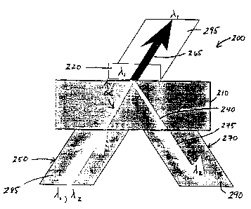
FIG. 2 illustrates an exemplary optical network assembly 200 that includes a
planar lightguide circuit (PLC) 210 and a filtering device 220. The exemplary
PLC 210
illustrated in FIG. 2 can include a first optical path 230 and a second
optical path 240.
The first optical path 230 can be connected to a first optical waveguide 250
that has a
first optical core 255. The filtering device 220 and the first optical path
230 can be
connected to a second optical waveguide 260 that has a second core 265. The
second
optical path 240 can be connected to a third optical waveguide 270 that has a
third core
275.
It is noted that the cores 255, 265, and 275 of the first, second, and third
optical
waveguides, respectively, each have arrow heads to designate the direction of
flow of
optical energy. In the actual physical embodiments of these waveguides, the
optical
cores are shaped similarly to the optical paths 230, 240 of the PLC 210.
Each optical path 230, and 240 of the PLC as well as the cores 255, 265 and
275
of the optical waveguides, can be made of a transparent material that has a
relatively
high index of refraction. The material 280, 285, 290, and 295 surrounding the
optical
12
SUBSTITUTE SHEET (RULE 26)
CA 02366200 2001-09-12
WO 00/55663 PCT/US00/06868
paths 230, 240 and cores 255, 265, and 275 can be made of a medium having a
lower
index of refraction relative to the cores and optical paths. This surrounding
material
may be different than that of the optical paths and cores or it may be a
similar material
wherein a dopant is introduced to alter its refractive index. Alternatively, a
dopant can
be introduced to either the core or optical path of a PLC or both in order to
alter the
refractive index of the core or path or both relative to the surrounding
material. The
optical paths and cores can be made of silica, plastic, high quality optical
glass such as
BK-7, or low-to-no expansion optical material such as ZERODUR glass.
PLC fabrication processes include ion exchange, flame hydrolysis, and reactive
ion etching. The waveguide can be imposed onto a substrate by depositing or
growing
a high index film on the substrate surface or by diffusing a dopant into the
substrate
surface. Etching and/or photolithographic techniques can be used to cast the
optical
paths within a PLC into desired circuit patterns.
Both optical waveguides 255, 265, and 275 and the optical paths of the PLC 210
can be designed to propagate single modes of optical energy so that the
optical energy
travels as a single wave front in order to substantially reduce attenuation
while
substantially increasing band width and transmission distances. The PLC 210
can
optimize the transfer of single mode optical energy propagation (referred to
as modal
transfer) between the optical waveguides 250, 260, and 270 and the PLC 210
itself.
The PLC 210 can minimize the modal disruption of optical energy that can
occur during the transfer of the optical energy between the optical waveguides
250,
260, 270, and the PLC 210. The PLC 210 can minimize modal disruption by
facilitating efficient alignment between the PLC 210 and the optical
waveguides 250,
260, and 270. In other words, the PLC's geometry permits rapid and efficient
alignment between the PLC 210 and the optical waveguides 250, 260, and 270.
The
PLC 210 can tolerate a certain amount of misalignment with the optical
waveguides
250, 260, and 270 without introducing any substantial optical losses. This
tolerance of
misalignment can translate into increased manufacturability of an optical
system that
includes the PLC 210 since dimensioning of the PLC 210 or light carrying
device or
both can be relaxed. An optical system can include the PLC 210 in combination
with
light carrying devices such as one or more optical fibers.
13
SUBSTITUTE SHEET (RULE 26)
CA 02366200 2001-09-12
WO 00/55663 PCT/US00/06868
Furthermore, a system including the PLC 210 can permit the use of passive
alignment techniques that can reduce time as well as expense for assembly of
the
system itself compared to conventional active alignment techniques that
require signal
propagation measurements. Additionally, the PLC 210 can be scaled to much
smaller
sizes compared to traditional expanded beam optics systems that require
additional
hardware such as lenses. The PLC 210 can interact with the filtering device
220
without the use of lenses.
Similar to the PLC 210, the filtering device 220 in combination with the PLC
210 can optimize the modal transfer between the PLC 210 and the second optical
waveguide 260. One way to optimize modal transfer between the PLC Z10 and
optical
waveguide 260 is to deposit the filtering device 220 directly on the PLC 210
itself or by
depositing the filtering device 220 directly on the end of the second optical
waveguide
260. Another way to optimize modal transfer between the PLC 210 and the second
optical waveguide 260 is to substantially reduce the thickness of the
filtering device
220 such that optical energy can be transferred to or from the PLC 210 in the
near field.
In other words, by substantially reducing the thickness of the filtering
device 220,
divergence of the optical energy propagating through the filtering device 220
can be
substantially reduced or become negligible. The interface between the light
carrying
device and PLC 210 can be made substantially small such that optical energy is
directed in a waveguide effectively formed between the PLC 210 and the light
carrying
device, such as second waveguide device 260.
The filtering device 220 can further optimize the modal transfer between the
PLC 210 and second optical waveguide 260 by increasing the packing density of
the
filtering device 220 such that the filtering device 220 approaches a bulk
density. In
other words, increasing packing density of the filtering device can
substantially reduce
or eliminate voids within the filtering device 220 that interfere with the
propagation of
optical energy. Such voids can sometimes trap light reflecting or light
disturbing
materials, such as water vapor, that can interfere with optical energy
propagation. The
filtering device 220 can be a dielectric, thin-film interference filter of
alternating
refractive index layers.
The filtering device 220 can have a packing density in excess of 90 percent.
In
other exemplary embodiments, the packing density for the filtering device 220
can be
14
SUBSTITUTE SHEET (RULE 26)
CA 02366200 2001-09-12
WO 00/55663 PCT/US00/06868
above 95 percent In further exemplary embodiments, the packing density can be
above
99 percent. In an exemplary embodiment, the filtering device can include
refractory
oxides. The filtering device 220 can also be a band pass filter covering at
least one
channel.
S However, the filtering device in other embodiments can also be a high-pass,
low-pass, or a band stop filter. The filtering device 220 can also be a rugate
filter. The
operating wavelength of the filtering device 220 can be a variety of
wavelengths,
including 830 nanometers, 1310 nanometers, and 1550 nanometer windows. The
slope
of the filtering device 220 relative to corresponding optical paths 230 and
240 can be
steep. In some exemplary embodiments, the filtering device 220 can be capable
of
differentiating between channels spaced less than two nanometers apart. In
another
exemplary embodiment, the filtering device can have a transmission greater
than 90
percent at a first wavelength channel and blocking at least 25 decibels (dB)
down at
adjacent channels spaced 1.8 nanometers away and at least 35 decibels at non-
adjacent
channels. Alternatively, the filtering device can also be a tunable filter.
The PLC 210 and filtering device 220 combination can separate optical energy
having at least two channels of information propagating at different
wavelengths
lambda one (Al) and lambda two (AZ). The PLC 210 and filtering device 220
combination can separate the optical energy propagating in the first optical
waveguide
250 into its discreet component beams that have wavelengths of lambda one (A,
) and
lambda two (AZ). The PLC 210 and optical filtering device 220 separate the
optical
energy by receiving the optical energy from the first optical waveguide 250
and
propagating the optical energy along the first optical path 230 of the PLC
210. The first
optical path 210 can propagate the optical energy towards the filtering device
220 that
has an operating wavelength of lambda one (A, ). The filtering device 220 can
be
disposed at an angle alpha relative to the first optical path 230 such that
all the optical
energy having a wavelength of lambda one (A~) will flow through the optical
filtering
device 220 into the second optical waveguide 260. The remaining optical energy
having a wavelength other than lambda one (A, ), such as a wavelength lambda
two
(A2), can then be reflected away from the optical filtering device 220 along
the second
optical path 240 of the PLC 210. The optical energy propagating along the
second
optical path 240 can then be carned further away by the third optical
waveguide 270.
SUBSTITUTE SHEET (RULE 26)
CA 02366200 2001-09-12
WO 00/55663 PCT/US00/06868
It is noted that the thickness of the optical filtering device 220 as
illustrated in
FIG. 2 has been exaggerated for illustration purposes only. In an actual
physical
embodiment, the optical filtering device 220 can be much thinner and dispose
substantially within the second optical waveguide 260 or attached directly to
a side of
the PLC such that its thickness is negligible compared to the planar surface
of the PLC
210.
The PLC Z10 can have a substantially rectangular shape as illustrated in FIG.
2.
However, other shapes are not beyond the scope of the present invention. The
PLC 210
can have two optical paths 230 and 240 as illustrated in FIG. 2. However, the
number
and orientation of optical paths are not limited to those shown in FIG. 2. The
number
of optical paths may be increased or decreased depending upon the application
of the
PLC 210. In an exemplary embodiment, the PLC 210 can be designed to couple to
one
or more single mode fibers. With the PLC 210, the separation between the PLC
210
and the optical waveguides 250, 260, and 270 can be minimized so as to
minimize
power loss and signal degradation associated with optical beam divergence. The
PLC
210 further minimizes the obliqueness of light incident on the filtering
device 220 so as
to maximize the filtering device performance.
The PLC 210 can be designed such that the longitudinal axis of the cores 255,
265, and 275 of the optical waveguides are substantially aligned with the
longitudinal
axis of the respective optical axes of the first and second optical paths 230,
240. This
design overcomes the long-standing challenge with optical structures
incorporating
single mode fibers where only a small percentage of the fiber end-face has
active
optical energy.
The direction of optical energy flowing through the optical waveguides 250,
260, and 270 and the PLC 210 in filtering device 220 is not limited to the
direction
illustrated in FIG. 2. The direction of the optical energy can be reversed
with respect to
the arrows illustrated in FIG. 2 such that "add" configuration can be made. In
other
words, instead of dropping a channel propagating along an optical beam having
a
wavelength of lambda one (A~), optical energy having wavelengths other than
lambda
one (A, ) can be added to a stream of optical energy (as will be discussed
below with
respect to FIG. 3). The PLC 210 and optical filtering device 220 are well
suited for
optical network technology. Such technology includes, but is not limited to,
16
SUBSTITUTE SHEET (RULE 26)
CA 02366200 2001-09-12
WO 00/55663 PCT/US00/06868
telecommunications, community antenna television (CATV) applications, computer
networking, and other similar types of applications.
FIG. 3 illustrates a single-channel drop-add configuration in which two PLC
optical filtering device combinations are used to drop a channel propagating
upon an
S optical beam having a wavelength of lambda one (A~) while adding optical
energy
having wavelengths other than lambda one (A~ ) to an optical beam having a
wavelength
of lambda one (A, ). In other words, the configuration illustrated in FIG. 3
has two
spectrally compatible band-pass filtering devices 220A and 220B that are
physically
opposing one another. The filtering devices may operate either on a single
channel or a
group of channels. The filtering devices 220A and 220B can also be constructed
as
high-pass or low-pass type filters. While dropping and adding the same channel
is
depicted, the drop and add channels can be unique. It is noted that the
angular
geometry of the light paths and end-faces of the PLC 210A and 210B are such
that the
end-faces of the PLC 210 and 210B can be within two parallel planes. The
opposing
optical waveguides can then be disposed in a parallel manner. The angle of
light
incident onto a filtering device end-face can equal the angle of reflected
light.
In the exemplary embodiment set forth in FIG. 3, optical energy A has optical
beams having wavelengths of lambda one (A1) and lambda two (AZ) that enter
into PLC
210A. The filtering device 220A operates at a wavelength of lambda one (A~)
such that
an optical beam B having a wavelength of lambda one (A,) can pass through the
filtering device 220A. The remaining optical energy C having an optical beam
with a
wavelength of lambda two (AZ) can be carried away by an optical waveguide
toward a
PLC 210B. An optical beam B with a wavelength of lambda one (A, ) is fed into
the
filtering device 220B such that the optical beam B passes through the optical
filtering
device 220B that operates at a wavelength of lambda one (A~). Optical energy C
having a wavelength of lambda two (AZ) is reflected off of the optical
filtering device
220B and combines with the optical beam B. The optical beam C and the optical
beam
B can combine to form optical energy A having wavelengths lambda one (A1) and
lambda two (AZ). While optical energy A exiting filtering device 210B and
optical
energy B entering filtering device 220B can have the same wavelengths as
optical
energy A and B entering and exiting filtering device 220A, the information
content
modulated on these respective optical beams can be different relative to each
other.
17
SUBSTITUTE SHEET (RULE 26j
CA 02366200 2001-09-12
WO 00/55663 PCT/US00/06868
That is, information content modulated on optical energy A at optical
filtering device
220A can be different then information content modulated on optical energy A
at
optical filtering device 220B. Alternatively, as apparent to those of ordinary
skill in the
art, information content at both optical filtering devices can be the same.
This
information modulation concept is also applicable to the remaining exemplary
embodiments of the present invention.
FIG. 4 illustrates another exemplary embodiment of a single-channel drop-add
configuration where the PLC 210C can form a cascade structure in which
multiple
reflections take place within the PLC 210C between multiple filtering devices
220A
and 220B. This exemplary embodiment can be referred to as a straight-line path
PLC
configuration because the optical paths of the PLC 210C can track the optical
energy's
path as it zigzags between filtering devices 220A and 220B. The resulting
functionality
of the embodiment illustrated in FIG. 4 is similar to that illustrated in FIG.
3. However,
the PLC 210C illustrated in FIG. 4 can have at least three optical paths that
interact
with at least two optical filtering devices 220A and 220B. Confining optical
energy
within the optical paths of the PLC 210C maintains intensity of the optical
channels
that are manipulated, and asserts control over modal patterns as well as
preserving
optical pulse quality.
FIG. 5 illustrates another alternate exemplary embodiment of a single-channel
drop-add configuration. However, in this alternate exemplary embodiment, the
second
optical path 240' of the PLC 210D can have a serpentine configuration such
that
control over the angle of incidence with respect to optical energy impinging
on the
filtering devices 220A and 220B can be controlled to minimize obliqueness.
This, in
turn, increases optimal performance of the optical filtering devices 220A and
220B.
Although the second optical path 240 is also illustrated in the exemplary PLC
210D, it
will be appreciated that the optical path 240 would not be present within the
PLC 210D
in an actual physical embodiment.
FIG. 6 illustrates another alternate exemplary embodiment that includes an
eight-channel dernultiplex or multiplex configuration. In this alternate
exemplary
embodiment, optical energy having wavelengths lambda one (A~) through lambda N
(AN) is fed into a PLC 210E. The optical filtering devices A-H filter out or
drop their
respective channels. After the optical energy is cascaded through the PLC
210E, the
18
SUBSTITUTE SHEET (RULE 26)
CA 02366200 2001-09-12
WO 00/55663 PCT/US00/06868
remaining optical energy, comprising wavelengths of lambda nine (A9) to lambda
N
(AN), can then be fed away from the PLC 210E. Although the embodiment
illustrated
in FIG. 6 support a demultiplexing architecture, a multiplexing function can
be
achieved by reversing the input and output of light energy relative to the PLC
210E.
FIG. 7 illustrates a further alternate exemplary embodiment that can provide a
four-channel drop-add configuration. In this exemplary embodiment, optical
energy
having wavelengths of lambda one (A1) through lambda N (AN) can be introduced
into
PLC Z10E. Channels having wavelengths lambda one (A,) through lambda four (A4)
are dropped and then reintroduced into the PLC 210E. In other words, as
respective
information channels having wavelengths lambda one (A, ) through lambda four
(A4)
are dropped, different signals that may operate upon the same wavelengths can
be
reintroduced into the PLC 210E. Therefore, optical energy having wavelengths
lambda
one (A~) through lambda N (AN) can be introduced into the PLC 210E and can
exit the
PLC 210E. However, it is noted that the information content of the optical
energy
1 S having wavelengths lambda one (A, ) through lambda N (AN) entering into
the PLC
210E can be different than the optical energy having wavelengths lambda one
(A, )
through lambda N (AN) exiting the PLC 210E.
FIG. 8 illustrates another alternate exemplary embodiment where the PLC 210E
is designed to drop four channels having wavelengths of lambda one (A,)
through
lambda four (A4). The optical energy is cascaded through the PLC 210E by a
plurality
of optical filtering devices A through D and focusing reflective elements E-H,
which
that can include concave mirrors.
Each mirror can correct for or reset beam divergence along the cascade path
within the PLC 210E and substantially reducing any need for collimation.
Fabrication
of the PLC 210E and focusing reflective elements E-H can be achieved by
molding or
a micro-machining materials, such as low-to-no expansion glass and optical
polymers
positioned within the optical cascade path. As optical energy reflects off a
respective
optical filtering device A-D, it can diverge or spread out relative to its
original path.
The concave mirrors E-H can substantially correct for this divergence by
refocusing the
optical energy to the next optical filtering device within the cascade.
FIG. 9 illustrates an additional alternate exemplary embodiment of the present
invention in which the PLC 210F includes a daisy-chained path construction.
Each
19
SUBSTITUTE SHEET (RULE 26)
CA 02366200 2001-09-12
WO 00/55663 PCT/US00/06868
optical path within the PLC 210F is curved to provide additional control over
the angle
of incidence onto a respective optical filtering device to minimize
obliqueness. In this
embodiment, optical channels propagating with wavelengths of lambda one (A1)
through lambda four (A4) can be dropped from the optical energy having
wavelengths
of lambda one (A1) through lambda N (AN).
FIG. 10 illustrates a dynamically and remotely configurable drop-add plus
optical cross-connect configuration. In the drop leg, lambda three (A3) of a
channel can
be fed back into the add leg as lambda three (A'3). The resulting loop not
only
bypasses the drop-add function but also provides a way to introduce dynamic
configuration capabilities and extended functionality. As illustrated, a
diverting
element 1000, such as a double-sided minor, can divert a channel's signal
content such
as lambda three (A3), out of the optical circuit and introduce new signal
content,
represented by lambda three (A' ~), back into the optical circuit. If the
diverting element
1000 is inserted at a point common to the branches of the two optical
circuits, then the
diverting device 1000 can operate as a configurable optical cross-connect.
Signals from the first circuit can be diverted to the second circuit.
Likewise,
signals from the second circuit can be diverted into the first optical
circuit. Activation
of the diverting element 1000 can be controlled by transmitting configuration
commands with primary optically encoded information across an optical circuit.
In this
manner, information packets and accompanying drop locations can be transmitted
across the optical network. One way to send this optical configuration
information is to
dedicate a channel to this function. A second way can be to tap off a fraction
of the
signal at a potential drop location. The signal may be sampled at pre-
determined times
without constant drain on network power.
Alternatively, a small portion of the optical power can be continually
monitored.
While a beam splitter can be used, less intrusive devices are available to
monitor the
optical signals. For example, commercial monitors are also available to
externally
access a fiber's active versus dark power status. However, such monitors lack
the
ability to read normally encoded, high-speed messages. By transmitting address
headers that contain device configuration instructions under a distinct
encoding regime,
detection power threshold can be reduced.
SUBSTITUTE SHEET (RULE 28)
CA 02366200 2001-09-12
WO 00/55663 PCT/US00/06868
Further, a header can be transmitted at a significantly slower light pulsing
rate
or distributed between several spectral channels. An optical circuit can
include an
optional monitor port having a beam splitter or similar component to tap off a
portion
of the light intensity for dynamic monitoring. Upon the recognition of signal
patterns,
the diverting device 1000 can be activated in response to the detection of
recognized
signal patterns by the monitoring port 500.
FIG. 11 illustrates the diverting element 1000 within the optical path of a
light
circuit. In accordance with this illustration, existing channel content
operating at a
wavelength lambda three (A'3), can be diverted while new channel content
operating at
lambda three (A3)' can be introduced into the light circuit.
In FIG. 12, the diverting element 1000 is outside an optical path of a light
circuit. The existing channel content operating at lambda three (A3) is
uninterrupted
while alternative channel content operating at lambda three (A'3) continues on
its path
through the optical path.
FIG. 13 illustrates an optical architecture for optical gain flattening or
spectral
amplification. An optical network spectral window of operations can be
defined, in a
large part, by the spectral range of amplification. Since amplification gain
can vary
dramatically with wavelength, the extent of each channel's amplification can
be defined
by its spectral position. This phenomenon can be particularly programmatic for
networks with multiple amplifiers, as the channel gain differential increases
with
multiple amplifications. In the assembly illustrated in FIG. 13, the channels
operating
at wavelengths lambda one (A,) through lambda four (A4) are attenuated
discretely by
gain flattening elements 1300 to flatten the gain of an extended spectral
range. This
approach can facilitate broadening of the spectral window of operation,
heightening the
channel count, and increasing a networks bandwidth.
The gain flattening elements 1300 can be represented as attenuators inserted
into the light path. Appropriate attenuation can be applied to each channel to
equalize
the signal strength across the spectral range of channels. One gain flattening
element
can be an attenuating fiber where the length of the fiber is set as
appropriate to realize
desired signal strength reduction. This attenuating fiber can be produced by
subjecting
the fiber to prolonged, intense ultraviolet radiation such that it "browns."
21
SUBSTITUTE SHEET (RULE 2B)
CA 02366200 2001-09-12
WO 00/55663 PCT/US00/06868
Similarly, absorbing material may be introduced into optical fiber materials.
For example, the OH content of an optical fiber's silica can be controlled to
set the
spectral attenuation level. Another approach is to include the attenuation
function
within a waveguided filtering element. Another approach is to apply an
attenuating
S coating onto the end-face surface of a waveguided filtering element
underneath a
filtering layer. A further approach is to include attenuation material within
the zigzag
depicted optical path within the PLC 210E. Another approach is to position the
channels with the highest power into locations with the lowest power transfer
efficiency, thereby achieving an inherent reduction of power that accompanies
beam
divergence in the zigzag optical path of a PLC 210E.
The assembly illustrated in FIG. 13 supports a discrete-channel approach to
signal amplification which is different from the common approach of
collectively
amplifying the channels. In the illustrated embodiment, the elements 1300
depicted can
be amplifiers that apply selective gain to each spectral region. The spectral
regions
may contain one or numerous channels. For example, this amplification can be
effective in transmitting and amplifying at both 1310 nanometers and 1550
nanometer
spectral windows. The device architecture illustrated iri FIG. 13 can provide
multiple
functions in a single integrated or modular unit.
FIG. 14 illustrates an add configuration that can be utilized to introduce
pump
laser light into an optical fiber or other waveguide such that in-the-
waveguide
amplification can be efficiently accomplished. In this embodiment, the optical
filtering
device operating at a wave length of lambda one (A, ) can efficiently pass the
pump
laser light operating at lambda one (A, ) into a pulse stream operating
wavelength at
lambda one (A ~ ) through lambda N (AN).
FIG. 15 illustrates another alternate exemplary embodiment of a multiplex
demultiplex configuration where optical energy having wavelengths lambda one
(Al)
through lambda N (AN) can be multiplexed at a multiplexer M and then
demultiplexed
at demultiplexer DM. The PLC 210, in combination with multiple optical
filtering
devices 220, can form the basis or the building blocks for the multiplexer M
and the
demultiplexer DM.
FIG. 16 illustrates an optical drop-add configuration where optical energy
operating with wavelengths of lambda one (A~) through lambda N (AN) can be
22
SUBSTITUTE SHEET (RULE 26)
CA 02366200 2001-09-12
WO 00/55663 PCT/US00/06868
multiplexed at multiplexer M and demultiplexed at DM. However, in between the
multiplexer M and demultiplexer DM, the channels lambda one (A~) and lambda
two
(AZ) can be dropped and manipulated. Signal content along channels lambda one
(A~)
and lambda four (A4) can be modified or simply monitored (remaining the same)
and
then reinserted back into the optical path between the multiplexer M and
demultiplexer
DM.
FIG. 17 illustrates an optical cross-connect configuration where two or more
networks can exchange information relative to one another. For example, a
first
network operating with wavelengths lambda one (A,) through lambda N (AN) can
exchange select channels of information with an optical network operating with
wavelengths lambda A (AA) through lambda zero (AD). Wavelength lambda one (A,
) is
substantially equal to wavelength lambda A (AA) except that each may contain
different
information relative to the other. In other words, information content of
wavelength
lambda one (A, ) can be different relative to the information content of
lambda A (AA)
but each wavelength can be substantially equal in magnitude. In this
embodiment,
channels lambda one (A,) and lambda four (A4) of the first network can be
replaced
with channels lambda A (AA) and lambda D (AD) of the second network and vice a
versa. The cross-connect device CC can be implemented by variations of single-
channel drop-add and cross-connect configurations, as discussed above.
FIG. 18 illustrates an alternate exemplary embodiment of a single-channel drop
or add where the PLC 2106 can be made from a single segment of an optical
material
suitable for an input or output leg. In this embodiment, a sharp bend 1800 of
an
appropriate angle can be introduced into a segment 1810 such that the segment
1800
and input leg 1810 are formed as an integral unit. This may be accomplished by
heating and bending, molding, or other methods of optical material
manipulation. The
filtering device can be attached to either the PLC 2106 or an output leg 1820.
Another
method of fabrication can be to appropriately position each leg and then mold
an
optical polymer between the legs so as to form the PLC 2106. In this assembly,
as
well as in related configurations, uncontrolled light scattering within a
light carrying
structure can degrade performance. A method of minimizing this unwanted light
in all
these assemblies can include coating appropriate surfaces with an opaque and a
light-
23
SUBSTITUTE SHEET (RULE 26)
CA 02366200 2001-09-12
WO 00/55663 PCT/US00/06868
absorbing coating. For example, the entire assembly can be encapsulated in a
carbon or
powdered metal-loaded epoxy.
FIG. 19 illustrates another alternate exemplary embodiment where the PLC
210H can be integrated into a bulk matrix. One method for forming this
structure can
be to utilize polymer molding techniques such as insert injection molding.
Another
method can be planar waveguide fabrication.
FIG. 20 illustrates another alternate exemplary embodiment where a PLC 210I
can have an optical path 2000 with a shape that is designed to collimate
optical energy
propagating there through. For single mode fibers operating in the near
infrared region,
the thickness of the optical filtering device 220 is significant relative to
the fiber core
size and outgoing light tends to diverge as it transmits through a filter
stack of the
optical filtering device. One method to address this situation is to shape the
optical
path 2000 on the opposite side of the optical filtering device 220 relative to
the core
2010 of an optical fiber 2020. As the optical path 2000 transfers light to the
optical
fiber 220, the optical path can be tapered so that light is projected
ultimately through
the filter stack of the optical filtering device 220 and into the fiber core
2010.
Alternatively (but not shown), the single mode fiber core 2010 can be shaped
to
collimate light energy propagating through the fiber 220 when the flow of the
optical
energy illustrated in FIG. 20 is reversed.
FIG.21 illustrates another alternate exemplary embodiment that includes a
mounting structure 2100 for receiving the PLC 210. The mounting structure 2100
includes a cavity 2110 shaped similarly to the PLC 210. The mounting structure
2100
may further include fiber alignment and attachment channels 2120 that
facilitate
passive alignment of optical waveguides with the PLC 210. The positions of
optical
waveguides in PLCs can be precisely maintained relative to each other in order
to
promote efficient optical energy transferred and to prevent modal disruption.
The
mounting structure can be constructed from materials and methods known within
the
semiconductor fabrication arts. These techniques will not be described but are
capable
of generating high-precision structures.
The depth at which the PLC 210 is inserted into the cavity 2110 can be an
important parameter as it can influence the efficiency of light transfer
between the
optical waveguides and the optical paths of the PLC 210. The positional
accuracy can
24
SUBSTITUTE SHEET (RULE 28)
CA 02366200 2001-09-12
WO 00/55663 PCT/US00/06868
be built into the assembly. One or more shim slabs can be used to assist in
positioning
the optical waveguides in the PLC 210. The fiber alignment and attachment
channels
2120 can be shaped to conform to symmetrical optical waveguides or,
alternatively, V-
grooves or rails can be employed. The diameters of the fiber alignment and
attachment
channels 2120 can be made slightly smaller than the diameter of an optical
waveguide
such that the optical waveguide can be held in place with the tension of the
fiber
alignment and attachment channels 2120. The PLC 210 and optical waveguides
(not
shown) can be fixed permanently to the mounting structure 2100 by
encapsulating the
entire assembly in an epoxy, a bonding agent, or similar material. Another
method for
forming the PLC 210 and optical waveguides to the mounting structure 2100 is
to mold
a polymer around the entire assembly.
FIG.22 illustrates another alternate exemplary embodiment that includes
another mounting structure 2220. The mounting structure 2220, which can be
configured for single-channel manipulation, includes V-grooves or similar
channels
2210 that can align multiple optical waveguides 2200. The substrate material
from
which the channels 2210 of the mounting structure 2220 can be formed may
include
low-to-no expansion glass, ceramic, silica, aluminum, silicon, or other
suitable
materials. The grooves or channels can be cut at appropriate angles relative
to one
another. Materials and techniques known to the semi-conductor arts can be used
to
form the channels 2210.
A block of optical material may be inserted into a gap 2230 between optical
waveguides 2200. This block (not shown) can assist in aligning the faces of
the optical
waveguides since only at the proper rotation will an element's face become co-
planar
with the block surface. Furthermore, the block (not shown) may have a high
refractive
index so as to minimize beam diverges during light cascade within a PLC. For
example, in the infrared region of the optical spectrum, silicon has desirable
characteristics. Cubic zirconium can be another high-refractive index material
and can
be used for outside of the transmission range of silicon. Optical polymers and
epoxies
can also be used. Low-to-no expansion glass such as that marketed under the
trade
name ZERODUR can be utilized to minimize thermal variation.
The mounting structure 2220 may also contain waveguide channels within its
structure. The block (not shown) may also have a refractive index gradient so
that light
SUBSTITUTE SHEET (RULE 26)
CA 02366200 2001-09-12
WO 00/55663 PCT/US00/06868
is steered within the gap. The block may also comprise properties such as
birefringence
in order to split and/or transmit light differently according to polarization.
Since
polarization dependency in filtering increases with the obliqueness of an
incidence
angle, this can facilitate compensating for interference filters spectral
variation with the
angle of incidence. Calcium fluoride is an example of a birefringent crystal.
The mounting structure 2220 can be permanently fixed by a number of devices.
Epoxy can be used to fill the gap and/or encapsulate the mounting assembly
2220.
Similarly, injection-molded optical polymers can be used. After the optical
waveguides
are positioned, they can be temporarily held in place. For example, a clamp
may be
used. Feeding test signals into the assembly and then micro-manipulating the
positioning (including rotation of the optical waveguides until the signals
are
optimized) can be a way of achieving optimum alignment. However, robotic or
other
automated manipulation can be used for volume-based productions. After a
position is
selected and the clamps of the optical waveguides are set, an epoxy or polymer
can be
injected around or into the assembly to provide encapsulation in environmental
isolation. Encapsulation can include hermetic techniques.
FIG. 23 illustrates a mounting structure 2300 that includes V-grooves 2310.
The V-grooves 2310 can facilitate efficient alignment between two optical
waveguides
or combination of optical waveguides and a PLC (not shown).
FIG. 24 illustrates an optical waveguide 2400 that can be used with PLC (not
shown) and optical filtering devices (not shown). In this embodiment, a fiber
Bragg
grating can be written into the optical fiber such that light is filtered both
by the grating
and an interference filter 2420 disposed at an end of the optical waveguide
2400. The
thin-film filter 2420 can operate over a broad spectral range and provides
only a
relatively coarse narrow spectral functionality. On the other hand, the fiber-
Bragg
grating 2410 can provide fine spectral resolution. Thus, the two filters can
compliment
one another. Thin-film interference filters, fiber Bragg gratings, and Mach-
Zender-
related interferometeric devices are three families of filtering technologies
that can be
important to optical networking. Thin-film interference filters can be the
most flexible
in terms of light manipulation and can have the best broad spectral
performance. The
latter two can be noteworthy for narrow band spectral performance.
26
SUBSTITUTE SHEET (RULE 26)
CA 02366200 2001-09-12
WO 00/55663 PCT/US00/06868
A goal of a general assembly architecture can be to provide a platform through
which multiple filtering technologies can be optimally combined. A related
goal can be
to provide ways to integrate multiple filters into an assembly in a series
fashion. Note
that light is precluded from resonating between the two filters 2420 and 2410
by
orienting one of the filters at an angle relative to the path of light
propagation. It is
further noted that the magnitude of the obliqueness of an angle of a thin-film
interference filter can be minimal because of the collimated aspect of the
light at that
point in the optical waveguide 2400. Tapered-based Mach-Zender technologies
can be
implemented but are not depicted in FIG. 24.
From the foregoing, it is apparent that the present invention has been
described
in relation to particular embodiments which are intended in all aspects to be
illustrative
rather than restrictive. Alternative embodiments will become apparent to those
skilled
in the art to which the present invention pertains without departing from its
spirit and
scope. Accordingly, the scope of the present invention is defined by the
appended
1 S claims rather than the foregoing description.
27
SUBSTITUTE SHEET (RULE 26)