Note : Les descriptions sont présentées dans la langue officielle dans laquelle elles ont été soumises.
CA 02366405 2002-O1-16
The present invention relates to a method of
manufacturing an optical waveplate, and a waveguide device
using the optical waveplate.
This application is a divisional application of
application 2,123,061, filed May 6, 1994.
Recently, various methods have been proposed for
transmission of a large quantity of information stably and
inexpensively. An optical communication system is one of
these methods. A representative example of this optical
communication system is a method (wavelength division
multiplexing system) in which light components having a
plurality of wavelengths and carrying their respective
signals are multiplexed into single light by a multiplexer
and transmitted to a remote place through an optical fiber.
The light is demultiplexed into the light components with
- their original wavelengths by a demultiplexer upon
reception, thereby detecting the individual signals. This
method can increase the communication capacity in
proportion to the multiplexing number of wavelengths and is
therefore a very effective method of increasing the
capacity. This method also can reduce the load on hardware
in an
- 1 -
CA 02366405 2002-O1-16
optical communication network connecting a number of
points and makes a more advanced network arrangement
possible by using a combination of a plurality of light
wavelengths, multiplexers, and demultiplexers in
addition to spatial wiring.
A system of the above sort requires a light
source which oscillates. at a plurality of wavelengths,
and a multi/demultiplexer for
multiplexing/demultiplexing Light. As the
multi/demultiplexer, a device using PLCs (Planar
Lightwave Circuits) consisting of optical waveguides
formed on a substrate has been developed as the most
realistic device from the point of view of a small size,
a light weight, and a high reliability. Of these PLCs,
a silica-based PLC fabricated by depositing a silica
glass film on a silicon substrate is expected as a
practical optical component, since it has a small
optical loss and consequently a high stability against
disturbance such as heat or vibrations.
The most serious problem in putting the
silica-based PLC into practical use is its polarization
dependence. That is, as mentioned above, this
silica-based PLC is manufactured by depositing a glass
film on a silicon substrate. Therefore, the difference
in thermal expansion coefficient between the glass film
and the silicon substrate makes a stress applied on an
optical waveguide in a direction parallel to the surface
- 2 -
CA 02366405 2002-O1-16
of the substrate differ from that in a direction
perpendicular to the substrate surface. Consequently,
the refractive index of the optical waveguide in the
direction parallel to the surface of the silicon
substrate becomes different from that in the direction
perpendicular to the substrate surface. This is termed
"waveguide birefringence". When, for example, an
asymmetrical Mach-Zender interferometer is constituted
by the silica-based PLC, this waveguide birefringence
gives rise to a problem that the optical path length
difference (a difference in refractive index x physical
length) of an arm constituting the interferometer
changes depending on the polarizing direction of light.
Consequently, the device characteristics change in
accordance with the polarized state of light. This
makes it impossible to apply the device to a system,
using a single-mode fiber.
This problem of the polarization dependence of
the PLC caused by the waveguide birefringence is not
inherent in a silica-based glass waveguide. That is,
all waveguides currently manufactured have this problem
because they also have waveguide birefringence, although
the degrees of waveguide birefringence differ from one
another. Examples of the waveguides are a titanium
in-diffused LiNb03 waveguide, a proton-exchanged LiNb03
waveguide, an ion-exchanged glass waveguide, a
semiconductor waveguide, a polycarbonate waveguide, a
- 3 -
CA 02366405 2002-O1-16
polyimide waveguide, a silicone resin waveguide, and an
epoxy resin waveguide.
As a method for compensating for the
birefringence of a silica-based optical waveguide, a
method of mounting amorphous silicon on top of a
waveguide and using the resultant stress is known. This
method, however, requires some additional steps, such as
a step of mounting amorphous silicon and a step of
trimming the amorphous silicon by using a laser, after a
sample is formed, in order to finely adjust the stress.
In addition, since it is difficult to compensate for the
waveguide birefringence across a wide area, individual
waveguides must be spaced apart from one another. It
is, therefore, impossible to apply this method to
waveguides integrated at a high density. As described
above, the method using the stress of amorphous silicon
has several practical problems.
Takahashi et al., on the other hand, have
developed a method of eliminating the polarization
dependence of the PLC by inserting a half waveplate
consisting of a rock crystal at the center of an optical
circuit of an arrayed-waveguide grating-type wavelength
multi/demultiplexer such that the optical principal axis
of the half waveplate forms an angle of 45° with a
substrate. (Hiroshi Takahashi et al., "Optics Letters,"
Vol. 17, No. 7, pp. 499-501 (1992)). Takahashi et al.
have also pointed out in Japanese Patent Prepublication
4 _
CA 02366405 2002-O1-16
No. 4-241304 that this method is also effective in
eliminating the polarization dependence of a Mach-Zender
interferometer, a ring resonator, a directional coupler,
and a phase modulator. This method of eliminating the
polarization dependence of an optical circuit by
inserting a rock-crystal half waveplate at the center of
the optical circuit realizes a high reliability for long
periods of time, has simple manufacturing steps, and can
be applied to all waveguides in addition to a
silica-based glass waveguide. Therefore, the method is
very effective compared to the above-mentioned method by
which amorphous silicon is mounted.
A rock crystal has a high heat resistance, a
high humidity resistance, and a high precision
processability and shows stable optical characteristics.
Therefore, a PLC incorporating a rock-crystal half
waveplate has a high reliability. However, this method
has a large drawback; that is, since there,is no
light-confining structure in the half waveplate and in a
groove for receiving the half waveplate, light
propagating through the waveguide is radiated from these
portions, resulting in loss of light. According to the
report by Takahashi et al., an excess loss of 5 dB is
produced when a half waveplate consisting of a rock
crystal is inserted into a 100-~m wide groove formed in
a waveguide with a specific refractive index difference
of 0.75. This value is extremely large comgared to a
- 5 -
CA 02366405 2002-O1-16
loss of 2 to 3 dB of the PLC itself. Consequently, it
has been impossible to apply the method to actual PLCs
from the point of view of the optical loss.
To obtain a PLC incorporating an optical
waveplate as a highly practical component, it is
important to decrease the excess loss produced by
insertion of the waveplate to 0.5 dB~or less {i.e., to
reduce the decrease in the light quantity to 10~ or
less).
Fig. 1 shows the result of simulation of the
excess loss performed by assuming that a light beam
emitted from the end face of an optical waveguide is a
Gaussian beam. This characteristic curve illustrated in
Fig. 1 shows that the excess loss is reduced to 0.3 dB
or less when the film thickness of an optical waveplate
is 20 ~m or less.
In a practical case, however, a loss of about
0.1 to 0.2 dB is unavoidable because of Fresnel
reflection or scattering at the end face of a waveplate.
When this fact is taken into consideration, therefore,
the film thickness of an optical waveplate must be 20 ~m
or smaller in order to reduce the excess loss as a
result of insertion of a waveplate to 0.5 dB or less.
To manufacture a half waveplate, with a wavelength (1.3
um, 1.55 Vim) currently used in long-distance optical
communication, to have a film thickness of 20 ~m or
smaller, the material of the waveplate is required to
- 6 -
CA 02366405 2002-O1-16
have an in-plane birefringence greater than at least
0.03. A rock-crystal half waveplate brings about a
large excess loss as described above because its
thickness is as large as 91 Vim. This large thickness
results from a small birefringence of a rock crystal of
0.0085 at a wavelength of 1.3 Vim. The use of a material
having a large birefringence makes it possible to
manufacture a thin waveplate, and this results in a
decreased excess loss. Calcite and titanium oxide are
known as inorganic single-crystal materials, other than
a rock crystal, having a large birefringence; both
calcite and titanium oxide have a birefringence larger
than that of a rock crystal. However, the rough of
calcite is expensive, and the thickness of a half
waveplate consisting of calcite becomes as very small as
4 ~m because the birefringence of calcite is large,
0.16, at a wavelength of 1.3 um. Since the hardness of
calcite is low (Mohs hardness: 2), it is. very difficult
to process calcite to have this small thickness. Even
if calcite can be thus processed, the product must be
handled with enough care. On the other hand, the
refractive index of titanium oxide is 2.62 to 2.90,
which is largely different from those of silica and
other optical waveguide materials. Therefore, when a
waveplate consisting of titanium oxide is inserted into
an optical waveguide, a loss caused by Fresnel
reflection at the end face of the waveguide is large.
CA 02366405 2002-O1-16
Consequently, the effect of decreasing the thickness of
a waveplate becomes insignificant. For the reasons
discussed above, neither calcite nor titanium oxide is a
suitable material to be inserted into a lightwave
circuit.
In order that a waveguide device in which a
half waveplate is inserted be used in practice, the heat
resistance and the humidity resistance of the waveplate
and the ease in handling the waveplate are also
important factors. For example, a waveguide device
fabricated on a single substrate is used not only as a
single component by itself but also as an "optical and
electronic hybrid interconnection" in combination with
other lightwave circuits and electric circuits
fabricated on the same substrate. The fabrication of
these photonic components involves a soldering step
performed at about 260°C and a step performed at a
temperature which temporarily exceeds 300°C. Therefore,
all the, materials used in the fabrication are required
to have a heat resistance of about 350°C.
An amorphous polymer plastic material is known
as a material which produces a birefringence.
Representative examples of such a polymer material are
polycarbonate and polyvinyl alcohol. These materials
produce an in-plane birefringence when films consisting
of the materials are drawn. In practice, large
retardation plates for use in liquid-crystal displays
_ 8 _
CA 02366405 2002-O1-16
are manufactured by using these polymer materials.
Retardation plates consisting of polystyrene, a
cellulose derivative, polyvinyl chloride, polypropylene,
an acrylic polymer, poly(amic acid), polyester, and an
ethylene-vinyl acetate copolymer saponified material are
also known. However, the polyvinyl alcohol-based
material and the cellulose derivative-based material
have a low humidity resistance, and the
polypropylene-based material is unsatisfactory in
14 toughness. The acryl-based material is difficult to
draw because its mechanical strength in the form of a
film is low. The polycarbonate-based material is poor
in chemical resistance.
The polyvinyl chloride material and the
polystyrene-based material are unsatisfactory
particularly in heat resistance and are therefore
inadequate for the purpose of the present invention.
Although the poly(amic acid)-based material and the
polyester-based material are considered to have a
relatively high heat resistance, none of these materials
has a heat resistance of 300°C or higher which is
required for waveguide devices. Also, a waveplate made
from any of these organic polymer materials is reduced
in birefringence due to activation of molecular motion
even at a temperature lower than its softening point
(glass transition temperature). This largely degrades
the characteristics as a waveplate. In addition, not a
- 9 _
CA 02366405 2002-O1-16
few of these organic polymer materials have a saturation
water absorption of 2 tb 3~. Since, however, water
molecules strongly absorb light with optical
communication wavelengths to increase the loss, the
material to be used as a waveplate must have as low a
water absorption as possible.
As discussed above, it is difficult to
manufacture waveplates that can be incorporated in
optical waveguides by using any of the conventionally
known polymer materials.
In summary, the problems of the conventional
optical waveplate techniques are as follows. That is,
for waveplates using inorganic single-crystal materials,
no material having an appropriate birefringence and
refractive index by which a waveplate can be
incorporated in a waveguide device is available. In
addition, these materials are difficult to process and
expensive. On the other hand, waveplates consisting of
plastic materials have problems in the heat resistance,
humidity resistance, and mechanical strength of a
material, and in the stability of in-plane
birefringence.
Summary of the Invention
It is, therefpre, a principal object of the
present invention to provide an optical waveplate which
can be readily manufactured and processed, has high heat
resistance, humidity resistance, flexibility, and
- 10 -
CA 02366405 2002-O1-16
mechanical strength, and also has a small film
thickness, a method of manufacturing this optical
waveplate, and a waveguide device using the waveplate.
It is another~object of the present invention
to provide a waveguide device having a sufficient
optical transparency.
To achieve the above objects, the present
inventors have focused attention on a polyimide optical
material which is applicable to optical waveguides, in-
IO view of the fact that the existing plastic optical
materials are unsatisfactory in heat resistance and
humidity resistance.
As for this polyimide optical material,
"Macromolecules" [T. Matsuura et al., Vol. 24,
pp. 5,001-5,005, 1991 and T. Matsuura et al., Vol. 25,
pp. 3,540-3,545, 1992] have already reported that
polyimide films having a heat resistance of 300°C or
higher, a low water absorption of 0.7$ or lower, and a
high optical transparency can be obtained by
synthesizing various fluorinated polyimides by using
2,2~-bis(trifluoromethyl)-4,4'-diaminobiphenyl as a
diamine component. T. Matsuura et al. have also
reported in Elec. Lett. Vol. 29, No. 24, pp. 2,107-2,109
that good optical waveguides for near-infrared light can
be formed by using, as a core and a cladding, a
polyimide synthesized by using a diamine and two
different types of tetracarboxylic dianhydrides. In
- 11 -
CA 02366405 2002-O1-16
addition, in "Macromolecules" [T. Matsuura et al.,
Vol. 25, pp. 5,858-5,860, 1992], S. Ando et al, have
reported a perfluorinated polyimide having no light
absorption peak in the entire optical communication
wavelength region (wavelength 1.0 to 1.7 Vim) and having
a heat resistance and a low water absorption equivalent
to those of fluorinated polyimides. This makes it
possible to provide a plastic optical material with a
very small loss even in a wavelength band in which
heat-resistant plastic materials are conventionally
difficult to use because they have absorption peaks
inherent in their molecular structures. It is also
found that polyimides can be readily processed and
handled because of their high flexibility and are
superior to other organic polymer materials in
toughness.
The gist of the present invention is to apply
these characteristic features of the polyimide optical
material to optical waveplates.
The basic concept of the present invention is
to form an optical waveplate by using a polyimide having
a film thickness of 20 ~m or smaller. An optical
waveplate with this arrangement is formed by thermally
imidizing a poly(amic acid) solution, which is
synthesized from a tetracarboxylic acid or its
derivative and a diamine, to have a film thickness of 20
- 12 -
CA 02366405 2002-O1-16
~m or less. In this case, the formed film is subjected
to uniaxial drawing or equivalent strain processing.
Although details of examples of this strain
processing will be discussed later as the examples of
the present invention, the processing will be briefly
explained below. That is, a poly(amic acid) solution
synthesized from a tetracarboxyl.ic acid or its
derivative and a diamine is coated on a substrate and
dried for a short time period. Thereafter, the
resultant film is peeled from the substrate with the
solvent contained in the film, and uniaxiall.y drawn.
The film is then fixed to a metal frame or the like and
thermally imidized. In another example, a poly(amic
acid? film is thermally imidized while it is uniaxially
drawn. In still another example, a poly(amic acid) film
is thermally imidized while it is fixed only in a
uniaxial drawing direction by a metal frame or the like.
In still another example, a poly(amic acid) solution is
coated on a substrate having an anisotropy of thermal
expansion coefficient in its plane, and the resultant
material is thermally imidized. In still another
example, a polyimide film is uniaxially drawn at a high
temperature of 300°C or higher. In still another
example, a polyimide film is thermally treated at a
temperature of 300°C or higher.
A waveguide device is constituted by using an
optical waveguide formed on a substrate and the
- 13 -
CA 02366405 2002-O1-16
polyimide waveplate characterized by the present
invention. As an example, a waveguide device is
constituted by inserting the optical waveplate of the
present invention into an optical waveguide such that
the.waveplate is either perpendicular to or inclined
from the longitudinal direction of the waveguide.
Alternatively, a half waveplate according to the present
invention is inserted into a waveguide such that the
optical principal axis of the half waveplate makes an
angle of 45° with a waveguide substrate.
Still another'waveguide device characterized
by the present invention comprises an optical waveguide
formed on a substrate and a polarization convertor
consisting of a polyimide optical waveplate arranged in
the middle of the optical path of the waveguide. This
polarization convertor consisting of the polyimide
optical wavepTate converts horizontal polarization (TE
mode: light having an electric field component in a
plane parallel to a substrate) contained in guided light
into vertical polarization (TM mode light having an
electric field component in a plane perpendicular to a
substrate) and vice versa. With this arrangement, the
dependence of the waveguide device on polarization can
be eliminated. Eliminating the polarization dependence
by replacing the horizontal polarization with the
vertical polarization and vice versa by inserting a half
waveplate in the middle of the optical path is identical
- 14 -
CA 02366405 2002-O1-16
in principle with the method disclosed in Japanese
Patent Prepublication No. 4-241304 mentioned earlier.
The characteristic feature of the present invention,
however, is that an excess loss caused by insertion of a
waveplate is largely decreased by applying a polyimide
optical waveplate with a film thickness of 20 um or less
to a waveguide device.
Still another waveguide device characterized
by the present invention comprises an optical waveguide
formed on a substrate af~d a polyimide optical waveplate.
This waveplate inserted into the waveguide consists of a
novel polarization beam splitter as a quarter waveplate.
This polarization beam splitter is so inserted that its
optical principal axis is either perpendicular or
parallel to the waveguide substrate. Although the
principle of operation of this invention will be
described in detail later by way of its examples, this
. quarter waveplate is not used as a polarization
convertor but used to cause the horizontal polarization
of guided light to have an optical path length longer or
shorter by a quarter wavelength than that for the
vertical polarization.
Still another waveguide device characterized
by the present invention comprises magnetic and
nonmagnetic waveguides formed on a substrate and a
polyimide optical waveplate. This waveplate inserted
into the waveguide consists of a novel circulator as a
- 15 -
CA 02366405 2002-O1-16
half waveplate. This circulator is so inserted that its
optical principal axis forms an angle of 22.5° or 67.5°
with the waveguide substrate. Although details of the
operating principle of this invention will also be
described later by way of the examples, this half
waveplate is used to rotate the polarizing direction of
guided light through 45° or 135°.
Still another waveguide device characterized
by the present invention comprises an optical waveguide
formed on a substrate and a polyimide optical waveplate.
This waveplate is in tight contact with the end face of
the waveguide so as to be perpendicular to or inclined
from the longitudinal direction of the waveguide. In
addition, a reflecting coat in formed on the side of the
waveplate not in contact with the end face of the
waveguide. This allows a single device to achieve both
the effect obtained by the waveplate and the reflection
of light. This waveplate can be a quarter waveplate.
In this case, the optical principal axis of this quarter
waveplate is so arranged as to make an angle of 45° with
the waveguide substrate. Although the operating
principle of this invention will also be described in
detail later by way of the examples, the quarter
waveplate and the reflecting coat formed on it are used
for the purposes of reflecting guided light and rotating
the polarizing direction of the light through 90°.
- 16 -
CA 02366405 2002-O1-16
In still another waveguide device
characterized by the present invention, a plurality of
several different types of waveguide devices as
described above are formed on the same substrate and
coupled to each other through optical.waveguides.
Note that a method of obtaining a
birefringence in the plane of a polyimide film is
described in K. Nakagawa, ",7. Appl. Polymer Sci.,"
Vol. 41, pp. 2,049-2,058, 1990. In this method, a film
consisting of a poly(amic acid) synthesized from a
pyromellitic dianhydride and 4,4'-diaminodiphenylether
is thermally imidized up to 160°C under a tensile stress
and then thermally treated up to 350°C. By this method,
drawing of a maximum of 83~ is possible, and a polyimide
film having a large in-plane birefringence of
approximately 0.18 (wavelength 0.633 ~tm) can be obtained
when drawing of 30~ or more is done: However, this
literature does not mention a method of controlling the
birefringence and the film thickness required to apply
polyimides to waveplates.
The present inventors, therefore, have
performed uniaxial drawing for films consisting of
poly(amic acids and polyimides, which are synthesized
by combining various acid anhydrides as derivatives of
tetracarboxylic acids with various diamines, by using
several different methods. Consequently, it is found
that the anisotropy of a refractive index
~- 17 -
CA 02366405 2002-O1-16
(birefringence) appears in the plane of a film in each
and every case. Thereafter, the present inventors have
made extensive studies on a method of controlling the
in-plane birefringence and the film thickness after
thermal imidization, and completed the optical
waveplates according to the present invention and the
method of manufacturing the waveplates.
Consequently, the present inventors have
completed the waveguide devices according to the present
invention by incorporating the various optical
waveplates obtained by the above method in waveguide
devices each comprising one or more optical waveguides
with birefringence formed on a substrate.
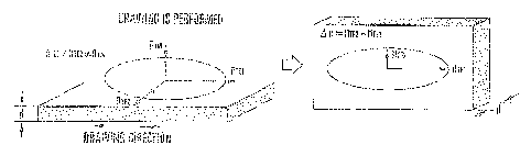
Figs. 2A and 2B are views each for explaining
the effect of drawing for a refractive index ellipsoid
representing the refractive index anisotropy of
polyimide films. Fig. 2A illustrates the retractive
index ellipsoid of a polyimide film not subjected to the
drawing, and Fig. 2B illustrates the refractive index
ellipsoid of a polyimide film subjected to the drawing.
When no drawing is performed, a refractive index
anisotropy (birefringence) is found in a direction
perpendicular to the plane of the film, but no
refractive index anisotropy is found in the direction of
the plane (n~i = n~E2). After the drawing is performed,
however, the birefringence is found not only in the
direction perpendicular to the plane but also in the
- 18 -
CA 02366405 2002-O1-16
direction of the plane ( nTgi # nTEZ ) , since the molecular
chains orient in the drawing direction. In the present
invention, of nTEi and nTBZ Perpendicular to each other,
nTEI which has a larger refractive index and the same
direction as the drawing direction is defined as the
optical principal axis. This axis is sometimes also
called a slow axis. If a value (retardation) calculated
by multiplying the in-plane birefringence (An: n~~ - nTSZ)
by the film thickness (d) is in agreement with a half or
quarter of the wavelength of a light beam, the film can
be used as a half or quarter waveplate. The film can
also be used as a waveplate of a higher order by
controlling the in-plane birefringence and the film
thickness.
Examples of the tetracarboxylic acid, and an
acid anhydride, an acid~chloride, and an ester as
derivatives of the tetracarboxylic acid for use in the
present invention are as follows. The names enumerated
below are names as tetracarboxylic acids. Examples are:
pyromellitic acid,
trifluoromethylpyromellitic acid,
pentafluoroethylpyromellitic acid,
bis~3,5-di(trifluoromethyl)phenoxy}pyromellitic acid,
2,3,3',4'-biphenyltetracarboxylic acid,
3,3',4,4'-tetracarboxydiphenylether,
2,3',3,4'-tetracarboxydiphenylether,
3,3',4,4'-benzophenonetetracarboxylic acid,
- 19 -
CA 02366405 2002-O1-16
2,3,6,7-tetracarboxynaphthalene,
1,4,5,7-tetracarboxynaphthalene,
1,4,5,6-tetracarboxynaphthalene,
3,3',4,4'-tetracarboxydiphenylmethane,
3,3',4,4'-tetracarboxydiphenylsulfone,
2,2-bis(3,4-dicarboxyphenyl)propane,
2,2-bis(3,4-dicarboxyph~nyl)hexafluoropropane,
5,5'-bis(trifluoromethyl)-3,3',4,4'-
tetracarboxybiphenyl,
2,2',5,5'-tetrakis(trifluoromethyl)-3,3',4,4'-
tetracarboxybiphenyl,
5,5'-bis(trifluoromethyl)-3,3',4,4'-
tetracarboxydiphenylether,
5,5'-bis(trifluoromethyl)-3,3',4,4'-
tetracarboxybenzophenone,
bis{trifluoromethyl)dicarboxyphenoxy}benzene,
bis{(trifluoromethyl)dicarboxyphenoxy}(trifluoromethyl)b
enzene,
bis(dicarboxyphenoxy)(trifluoromethyl)benzene,
bis(dicarboxyphenoxy)bis(trifluoromethyl)benzene,
bis(dicarboxyphenoxy)te~rakis(trifluoromethyl)benzene,
3,4,9,10-tetracarboxyperylene,
2,2-bis{4-(3,4-dicarboxyphenoxy)phenyl}propane,
butanetetracarboxylic acid,
cyclopentanetetracarboxylic acid,
2,2-bis{4-(3,4-
dicarboxyphenoxy)phenyl}hexafluoropropane,
bis{(trifluoromethyl)dicarboxyphenoxy}biphenyl,
bis{(trifluoromethyl)dicarboxyphenoxy}bis(trifluoromethy
1)biphenyl,
bis{(trifluoromethyl)dicarboxyphenoxy}diphenylether,
- 20 -
CA 02366405 2002-O1-16
bis(dicarboxyphenoxy)bis(trifluoromethyl)biphenyl,
bis(3,4-dicarboxyphenyl)dimethylsilane,
1,3-bis(3,4-dicarboxyphenyl)tetramethyldisiloxane,
1,4-bis(3,4-
dicarboxytrifluorophenoxy)tetrafluorobenzene,
1,4-bis(3,4-
dicarboxytrifluorophenoxy)octafluorobiphenyl,
1,4-difluoropyromellitic acid,
1-trifluoromethyl-4-fluoropyromellitic acid,
1,4-di(trifluoromethyl)pyromellitic acid,
1-pentafluoroethyl-4-fluoropyromellitic acid,
1-pentafluoroethyl-4-trifluoromethylpyromellitic acid,
1,4-di(pentafluoroethyl)pyromellitic acid,
1-pentafluorophenyl-4-fluoropyromellitic acid,
1-pentafluorophenyl-4-trifluoromethylpyromellitic acid,
1-pentafluorophenyl-4-pentafluoroethylpyromellitic acid,
1,4-di(pentafluorophenyl)pyromellitic acid,
1-trifluoromethoxy-4-fluoropyromellitic acid,
1-trifluoromethoxy-4-trifluoromethylpyromellitic acid,
1-trifluoromethoxy-4-pentafluoroethylpyromellitic acid,
1-trifluoromethoxy-4-pentafluorophenylpyromellitic acid,
1,4-di(trifluoromethoxy)pyromellitic acid,
1-pentafluoroethoxy-4-fluoropyromellitic acid,
1-pentafluoroethoxy-4-trifluoromethylpyromellitic acid,
1-pentafluoroethoxy-4-pentafluoroethylpyromellitic acid,
1-pentafluoroethoxy-4-pentafluorophenylpyromellitic
acid,
1-pentafluoroethoxy-4-trifluoromethoxypyromellitic acid,
1,4-di(pentafluoroethoxy)pyromellitic acid,
- 21 -
CA 02366405 2002-O1-16
1-pentafluorophenoxy-4-fluoropyromellitic acid,
1-pentafluorophenoxy-4-trifluoromethylpyromellitic acid,
1-pentafluorophenoxy-4-pentafluoroethylpyromellitic
acid,
1-pentafluorophenoxy-4-pentafluorophenylpyromellitic
acid,
1-pentafluorophenoxy-4-trifluoromethoxypyromellitic
acid,
1-pentafluorophenoxy-4-pentafluoroethoxypyromellitic
acid,
1,4-di(pentafluorophenoxy)pyromellitic acid,
hexafluoro-3,3',4,4'-biphenyltetracarboxylic acid,
hexafluoro-3,3',4,4'-biphenylethertetracarboxylic acid,
hexafluoro-3,3',4,4'-benzophenonetetracarboxylic acid,
bis(3,4-dicarboxytrifluorophenyl)sulfone,
bis(3,4-dicarboxytrifluorophenyl)sulfide,
bis(3,4-dicarboxytrifluorophenyl)difluoromethane,
1,2-bis(3,4-dicarboxytrifluorophenyl)tetrafluoroethane,
2,2-bis(3,4-dicarboxytrifluorophenyl)hexafluoropropane,
1,4-bis(3,4-dicarboxytrifluorophenyl)tetrafluorobenzene,
3,4-dicarboxyfluorophenyl-3',4'-
dicarboxytrifluorophenoxy-difluoromethane,
bis(3,4-dicarboxytrifluorophenoxy)difluoromethane,
1,2-bis(3,4-dicarboxytrifluorophenoxy)tetrafluoroethane,
2,.2-bis(3,4-dicarboxytrifluorophenoxy)hexafluoropropane,
1,4-bis(3,4-
dicarboxytrifluorophenoxy)tetrafluorobenzene,
2,3,6,7-tetracarboxy-tetrafluoronaphthalene,
2,3,6,7-tetracarboxy-hexafluoroanthracene,
2,3,6,7-tetracarboxy-hexafluorophenanthrene,
- 22 -
CA 02366405 2002-O1-16
2,3,6,7-tetracarboxy-tetrafluorobiphenylene,
2,3,7,8-tetracarboxy-tetrafluorodibenzofuran,
2,3,6,7-tetracarboxy-tetrafluoroanthraquinone,
2,3,6,7-tetracarboxy-pentafluoroanthrone,
2,3,7,8-tetracarboxy-tetrafluorophenoxathiin,
2,3,7,8-tetracarboxy-tetrafluorothianthrene, and
2,3,7,8-tetracarboxy-tetrafluorodibenzo[b,e]l,4dioxane.
Examples of the diamine for use in the present
invention are:
m-phenylenediamine,
2,4-diaminotoluene,
2,4-diaminoxylene,
2,4-diaminodurene,
4-(1H,1H,11H-eicosafluoroundecanoxy)-1,3-diaminobenzene,
4-(1H,1H-perfluoro-1-butanoxy)-1,3-diaminobenzene,
4-(1H,1H-perfluoro-1-heptanoxy)-1,3-diaminobenzene,
4-(1H,1H-perfluoro-1-octanoxy)-1,3-diaminobenzene,
4-pentafluorophenoxy-1,3-diaminobenzene,
4-(2,3,5,6-tetrafluorophenoxy)-1,3-diaminobenzene,
4-(4-fluorophenoxy)-1,3-diaminobenzene,
4-(1H,1H,2H,2H-perfluoro-1-dodecanoxy)-1,3-
diaminobenzene,
p-phenylenediamine,
2,5-diaminotoluene,
2,3,5,6-tetramethyl-p-phenylenediamine,
2,5-diaminobenzotrifluoride,
bis(trifluoromethyl)phenylenediamine,
diaminotetra(trifluoromethyl)benzene,
- 23 -
CA 02366405 2002-O1-16
diamino(pentafluoroethyl)benzene,
2,5-diamino(perfluorohexyl)benzene,
2,5-diamino(perfluorobutyl)benzene,
benzidine,
2,2'-dimethylbenzidine,,
3,3'-dimethylbenzidine,
3,3'-dimethoxybenzidine,
2,2'-dimethoxybenzidine,
3,3',5,5'-tetramethylbenzidine,
3,3'-diacetylbenzidine,
2,2'-bis(trifluoromethyl)-4,4'-diaminobiphenyl,
3,3'-bis(trifluoromethyl)-4,4'-diaminobiphenyl,
4,4'-diaminodiphenylether,
4,4'-diaminodiphenylmethane,
4.4'-diaminodiphenylsulfone,
2,2'-bis(p-aminophenyl)propane,
3,3'-dimethyl-4,4'-diaminodiphenylether,
3,3'-dimethyl-4,4'-diaminodiphenylmethane,
1,2-bis(anilino)ethane,
2,2-bis(p-aminophenyl)hexafluoropropane,
1,3-bis(anilino)hexafluoropropane,
1,4-bis(anilino)octafluorobutane,
1,5-bis(anilino)decafluoropentane,
1,7-bis(anilino)tetradecafluoroheptane,
2.2'-bis(trifluoromethyl)-4,4'-diaminodiphenylether,
3,3'-bis(trifluoromethyl)-4,4'-diaminodiphenylether,
3,3',5,5'-tetrakis(trifluoromethyl)-4,4'-
diaminodiphenyiether, '
- 24 -
CA 02366405 2002-O1-16
3,3'-bis(trifluoromethyl)-4,4'-diaminobenzophenone,
4,4"-diamino-p-terphenyl,
1,4--bis(p-aminophenyl)benzene,
p-bis(4-amino-2-trifluoromethylphenoxy)benzene,
bis(aminophenoxy)bis(trifluoromethyl)benzene,
bis(aminophenoxy)tetrakis(trifluoromethyl)benzene,
4,4"'-diamino-p-quaterphenyl,
4,4'-bis(p-aminophenoxy)biphenyl,
2,2-bis{4-(p-aminophenoxy)phenyl}propane,
4,4'-bis(3-aminophenoxyphenyl)diphenylsulfone,
2,2-:bis{4-(4-aminophenoxy)phenyl}hexafluoropropane,
2,2-bis{4-(3-aminophenoxy)phenyl}hexafluoropropane,
2,2-bis{4-(2-aminophenoxy)phenyl}hexafluoropropane,
2,2-bis{4-(4-aminophenoxy)-3,5-
dimethylphenyl}hexafluoropropane,
2,2-bis{4-(4-aminophenoxy)-3,5-
ditrifluoromethylphenyl}hexafluoropropane,
4,4'-bis(4-amino-2-trifluoromethylphenoxy)biphenyl,
4,4'-bis(4-amino-3-trifluoromethylphenoxy)biphenyl,
4,4'-bis(4-amino-2-
trifluoromethylphenoxy)diphenylsulfone,
4,4'-bis(3-amino-5-
trifluoromethylphenoxy)diphenylsulfone,
2,2-bis{4-(4-amino-3-
trifluoromethylphenoxy)phenyl}hexafluoropropane,
bis{(trifluoromethyl)aminophenoxy}biphenyl,
bis[{(trifluoromethyl.)aminophenoxy}phenyl]hexafluoroprop
ane,
diaminoanthraquinone,
1,5-diaminonaphthalene,
- 25 -
CA 02366405 2002-O1-16
2,6-diaminonaphthalene,
bis[~2-(aminophenoxy)phenyl}hexafluoroisopropyl]benzene,
bis(2,3,5,6-tetrafluoro-4-aminophenyl)ether,
bis(2,3,5,6-tetrafluoro-4-aminophenyl)sulfide,
1,3-bis(3-aminopropyl)tetramethyldisiloxane,
1,4-bis(3-aminopropyldimethylsilyl)benzene,
bis(4-aminophenyl)diethylsilane,
tetrafluoro-1,2-phenylenediamine,
tetrafluoro-1,3-phenylenediamine,
tetrafluoro-1,4-phenylenediamine,
hexafluoro-1,5-diaminonaphthalene,
hexafluoro-2,6-diaminonaphthalene,
3-trifluoromethyl-trifluoro-1,2-phenylenediamine,
4-trifluoromethyl-trifluoro-1,2-phenylenediamine,
2-trifluoromethyl-trifluoro-1,3-phenylenediamine,
4-trifluoromethyl-trifluoro-1,3-phenylenediamine,
5-trifluoromethyl-trifluoro-1,3-phenylenediamine,
2-trifluoromethyl-trifluoro-1,4-phenylenediamine,
3,4-bis{trifluoromethyl)-difluoro-1,2-phenylenediamine,
3,5-bis(trifluoromethyl)-difluoro-1,2-phenylenediamine,
2,4-bis(trifluoromethyl)-difluoro-1,3-phenylenediamine,
4,5-bis(trifluoromethyl)-difluoro-1,3-phenylenediamine,
4,6-bis(trifluoromethyl)-difluoro-1,3-phenylenediamine,
2,3-bis(trifluoromethyl)-difluoro-1,4-phenylenediamine,
2,5-bis(trifluoromethyl)-difluoro-1,4-phenylenediamine,
3,4,5-tris(trifluoromethyl)-fluoro-1,2-phenylenediamine,
3,4,6-tris(trifluoromethyl)-fluoro-1,2-phenylenediamine,
- 26 -
CA 02366405 2002-O1-16
2,4,5-tris(trifluoromethyl)-fluoro-1,3-phenylenediamine,
2,4,6-tris(trifluoromethyl)-fluoro-1,3-phenylenediamine,
4,5,6-tris(trifluoromethyl)-fluoro-1,3-phenylenediamine,
tetrakis(trifluoromethyl)-1,2-phenylenediamine,
tetrakis(trifluoromethyl)-1,3-phenylenediamine,
tetrakis(trifluoromethyl)-1,4-phenylenediamine,
3-pentafluoroethyl-trifluoro-1,2-phenylenediamine,
4-pentafluoroethyl-trifluoro-1,2-phenylenediamine,
2-gentafluoroethyl-trifluoro-1,3-pheny~lenediamine,
4-pentafluoroethyl-trifluoro-1,3-phenylenediamine,
5-pentafluoroethyl-trifluoro-1,3-phenylenediamine,
2-pentafluoroethyl-trifluoro-1,4-phenylenediamine,
3-trifluoromethoxy-trifluoro-1,2-phenylenediamine,
4-trifluoromethoxy-trifluoro-1,2-phenylenediamine,
2-trifluoromethoxy-trifluoro-1,3-phenylenediamine,
4-trifluoromethoxy-trifluoro-1,3-phenylenediamine,
5-trifluoromethoxy-trifluoro-1,3-phenylenediamine,
2-trifluoromethoxy-trifluoro-1,4-phenylenediamine,
3,3'-diamino-octafluorobiphenyl,
3.4'-diamino-octafluorobiphenyl,
4,4'-diamino-octafluorobiphenyl,
2,2'-bis(trifluoromethyl)-4,4'-
diaminohexaf luorobiphen~rl,
3,3'-bis(trifluoromethyl)-4,4~-
diaminohexafluorobiphenyl,
bis(3 -amino-tetrafluorophenyl)ether,
3,4'-diamino-octafluorobiphenylether,
bis(4-amino-tetrafluorophenyl)ether,
- 27 -
CA 02366405 2002-O1-16
3,3'-diamino-octafluorobenzophenone,
3,4'-diamino-octafluorobenzophenone,
4,4'-diamino-octafluorobenzophenone,
bis(3-amino-tetrafluorophenyl)sulfone,
3,4'-diamino-octafluorobiphenylsulfone,
bis(4-amino-tetrafluorophenyl)sulfone,
bis(3-amino-tetrafluorophenyl)sulfide,
3,4'-diamino-octafluorobiphenylsulfide,
bis(4-amino-tetrafluorophenyl)sulfide,
bis(4-aminotetrafluorophenyl)difluoromethane,
1,2-bis(4-aminotetrafluorophenyl)tetrafluoroethane,
2,2-bis(4-aminotetrafluorophenyl)hexafluoropropane,
4,4"-diamino-dodecafluoro-p-terphenyl,
4-amino-tetrafluorophenoxy-4'-amino-tetrafluorophenyl-
difluoromethane,
bis(4-amino-tetrafluorophenoxy)-difluoromethane,
1,2-bis(4-amino-tetrafluorophenoxy)-tetrafluoroethane,
2,2-bis(4-amino-tetrafluorophenoxy)-hexafluoropropane,
1,4-bis(4-amino-tetrafluorophenoxy)-tetrafluorobenzene,
2,6-diamino-hexafluoronaphthalene,
2,6-diamino-octafluoroanthracene,
2,7-diamino-octafluorophenanthrene,
2,6-diamino-hexafluorobiphenylene,
2,7-diamino-hexafluorobenzofuran,
2,6-diamino-hexafluoroanthraquinone,
2,6-diamino-octafluoroanthrone,
2,7-diamino-hexafluorophenoxathiin,
2,7-diamino-hexafluorothianthrene, and
- 28 -
CA 02366405 2002-O1-16
2,7-.diamino-tetrafluorodibenzo[b,e)l,4dioxane.
To achieve a birefringence exceeding 0.03
required to realize a polyimide optical waveplate with a
film thickness of 20 ~m or smaller, which is
characterized by the present invention, by drawing at a
practical draw ratio, it is preferable that one or both
of the tetracarboxylic acid or its derivative and the
diamine have a highly linear structure in which the
skeleton or main chain structure has no rotatable bond
or has only one rotatable bond. For example, if two or
more rotatable bonds are contained in the skeleton of
the diamine (i:e., if any of an ether group, a thioether
group, a methylene group, a sulfone group, a carbonyl
group, an isopropylidene group, and a
hexafluoroisopropyiidene group is contained), preferable
usable examples of the tetracarboxylic acid are a
pyromellitic acid whose skeleton consists of one benzene
ring, a derivative of this pyromellitic acid in which
two hydrogen atoms bonded to that benzene ring are
substituted with another organic substituent or halogen,
2,3,3',4'-biphenyltetracarboxylic acid whose skeleton is
a biphenyl structure, and a derivative of this
2,3,3',4'-biphenyltetracarboxylic acid in which four
hydrogen atoms bonded to the benzene ring of that
biphenyl structure are substituted with another organic
substituent or halogen. If the skeleton of an acid
anhydride contains two or more rotatable bonds, examples
- 29 -
CA 02366405 2002-O1-16
of the di.amine are preferably a diaminobenzene whose
skeleton consists of one benzene ring, a derivative of
this diaminobenzene in which four hydrogen atoms bonded
to that benzene ring are substituted with another
organic substituent or halogen, and a derivative in
which the skeleton is a biphenyl structure and some or
all of hydrogen atoms bonded to the benzene ring of that
biphenyl structure are substituted with another organic
group or halogen. As will be presented later in the
examples of the present invention, however, even the use
of a diamine whosa skeleton is a biphenyl structure
cannot achieve a birefringence greater than 0.03 in some
cases if the skeleton of an acid anhydride is
exceedingly flexible. Therefore, it is more favorable
that both of the tetracarboxylic acid or its derivative
and the diamine have a highly linear structure in which
the skeleton has no rotatable bond or has only one
rotatable bond.
In addition, to prevent a decrease in
transparency to near-infrared light as a result of the
absorption of moisture in the air and to extend the
high-optical transparency region toward the
low-wavelength side in a visible region, it i:s
preferable that a fluorine atom be bonded to one or both
of the tetracarboxylic acid or its derivative and the
diamine as the materials. Especially when
2,2'-bis(trifluoromethyl)-4,4'-diaminodiphenyl is used
- 30 -
CA 02366405 2002-O1-16
as the diamine, as will be presented later in the
examples of the present invention later, it is possible
to obtain a polyimide film having a large in-plane
birefringence, a high optical transparency, and a low
S water absorption. Also, to manufacture an optical
waveplate whose absorption loss to near-infrared light
containing optical communication wavelengths is reduced
to a minimum possible limit, it is preferable that one
or both of the tetracarboxylic acid or its derivative
and the diamine, as the materials, be completely
fluorinated except for an amino group.
A poly(amic acid) solution or film is
manufactured by causing the tetracarboxylic acid or its
derivative and the diamine as described above to react
with each other. A method of manufacturing the
poly(amic acid) can be the same as conventional
poly(amic acid) manufacturing methods. Generally, a
dianhydride of a tetracarboxylic acid is reacted with an
equal molar quantity of a diamine in a polar organic
solvent such as N-methyl-2-pyrrolidone,
N,N-dimethylacetamide, or N,N-dimethylformamide. These
materials can also be reacted in a vacuum, in a vapor
phase, or at a high pressure in the absence of a
solvent. In the present invention, both the
tetracarboxylic acid or its derivative and the diamine
need not be single compounds; that is, it is possible to
mix a plurality of tetracarboxylic acids or their
- 31 -
CA 02366405 2002-O1-16
derivatives and diamines. In this case, the total
number of moles of a plurality of diamines or one
diamine must be equal or nearly equal to that of a
plurality of tetracarboxylic acids or their derivatives
or one tetracarboxylic acid or its derivative.
The resultant~poly(amic acid) is then imidized
to synthesize a poly.imide. This synthesis can be
performed by conventional polyimide synthesizing methods
including thermal imidization. In the present
invention, however, it is also possible to obtain a
mixture of polyimides by imidizing a plurality of
poly(amic acids in the form of a mixture, as well as
imidizing a single poly(amic acid).
As a method of manufacturing a polyimide
having birefringence in the plane of a film, it is
effective to simultaneously or continuously perform
uniaxial drawing and thermal imidization for a poly(amic
acid) film containing a certain amount of a,solvent.
Specific methods that are found to be effective by the
examples of the present invention are:
a method of uniaxially drawing a poly(amic
acid) film and then thermally imidizing the
film with the film be fixed in either a
uniaxial or biaxial directions by a metal
frame or the like;
a method of simultaneously performing drawing
and imidization by performing thermal
- 32 -
CA 02366405 2002-O1-16
imidization for a poly(amic acid) film while
the film is subjected to a tensile stress in a
uniaxial direction;
a method of simultaneously performing drawing
and imidization by using shrinkage of a
poly(amic acid) film and evaporation of a
solvent caused by imidization taking place in
the process of thermal imidization performed
for the film by fixing it in only a uniaxial
direction by a metal frame or the like; and
a method of performing drawing and imidization
by using the anisotropy of thermal expansion
coefficient of a substrate occurring in the
process of thermal imidization performed for a
poly(amic acid) solution coated on the
substrate having the anisotropy of thermal
expansion coefficient in its plane.
Performing the drawing simultaneously with the
thermal imidization is effective to obtain a large
in-plane birefringence. However, performing the drawing
for a polyimide film which is already imidized and has
no in-plane birefringence is ineffective, since the
consequent in-plane birefringence is small compared to
that obtained by the above method. For a polyimide film
which is already imidized and yet has a retardation
close to the target value, however, performing the
drawing again at a high temperature of 300°C or higher
- 33 -
CA 02366405 2002-O1-16
is effective as a retardation adjusting method. It is
also effective as a more precise retardation adjusting
method to perform a thermal treatment for a polyimide
film of the above sort at a high temperature of 300°C or
higher with no stress applied. This method makes use of
a phenomenon in which a polyimide having a rigid
structure spontaneously orients at a high temperature to
increase the birefringence. Note that when any of these
methods is to be used, it is preferable to adjust the
drawing conditions or the temperature while externally
monitoring the retardation of that polyimide film.
One example of a method of uniaxially drawing
a poly(amic acid) film at around room temperature is a
method in which a poly(amic acid) solution is coated on
a substrate, the solvent is dried to some extent, and
then the film is peeled from the substrate and drawn.
Other examples are a method in which a poly(amic acid)
solution is coated on a readily drawable polymer (e. g.,
polyvinyl alcohol or polycarbonate) substrate, the
solvent is dried to some extent; the poly(amic acid)
film is drawn together with the substrate, and then the
film is peeled from the substrate; and a method in which
a poly(amic acid) film peeled from a substrate is dipped
in a solvent mixture of a good solvent and a poor
solvent and drawn after the swell proceeds to a certain
degree. Some other methods than the methods herein
mentioned are also possible as the method of uniaxial
- 34 -
CA 02366405 2002-O1-16
drawing of a poly(amic acid) at around room temperature
or uniaxial drawing of a poly(amic acid) film at a high
temperature. That is, any method is usable in principle
provided that the molecular chains of the poly(amic
acid) or polyimide orient in the uniaxial direction. An
example is a method in which a poly(amic acid) solution
is coated on a substrate consisting of a heat-resistant
plastic or a metal, the solvent is dried to some extent,
and then the film is thermally imidized while it is
drawn under a stress by bending it together with the
substrate. Normal drawing operations using a roll
drawing machine, a tenter drawing machine, and the like
are also considered to be effective.
As the substrate having an anisotropy of
thermal expansion coefficient in its plane, calcite is
effective as will be described later in the examples of
the present invention. Other effective examples are
single-crystal materials such as a rock crystal, lithium
niobate, lithium tantalite, and titanium oxide, and
metal materials such as a fiber reinforced metal (FRM)
in which glass fiber or the like is embedded in the
uniaxial direction, as inorganic materials; and
liquid-crystal polyester, liquid crystal polyacrylate,
and fiber reinformed plastic (FRP) in which glass fiber
or the like is embedded in the uniaxial direction, as
organic materials. In addition, a piezoelectric
material that expands or contracts in one direction upon
- 35 -
CA 02366405 2002-O1-16
being applied with a voltage and a pyroelectric material
that expands or contracts in one direction upon being
heated can also be considered to be effective as the
substrate.
To obtain an optical waveplate consisting of a
polyimide, it is normally required to match the
retardation of the polyimide to a half or quarter of the
wavelength of guided light. Therefore, control of the
thickness of a film is important as well as control of
the in-plane birefringence. The control of the film
thickness of a polyimide is generally done by optimizing
the spin-coating conditions of a poly(amic acid)
solution as a precursor of the film. A film requiring
more accurate film thickness control can be formed by
shaping a drawn polyimide film, with a thickness
slightly larger than a design value, to have a
predetermined thickness by using reactive ion etching,
W asher, or oxygen asher.
The polyimide optical waveplate according to
the,present invention is manufactured for the purpose of
primarily inserting it in the middle of the optical path
of an optical waveguide or of a waveguide device.
However, this polyimide optical waveplate can also be
used intact as a conventional optical waveplate. It is
also possible to use the polyimide optical waveplate as
an optical retardation plate by adjusting the
retardation of the plate to any given value rather than
- 36 -
CA 02366405 2002-O1-16
a half or quarter of the wavelength of guided light. In
addition, since polyimides have a heat resistance of
300°C or higher, it is possible to form a thin film or a
multilayered film of a metal, a semiconductor, or a
dielectric on the surface of a polyimide by sputtering
or vapor deposition. Any of these films can be used as
a reflecting film or a filter for cutting off light
having a specific wavelength.
Brief Description of the Drawings
Fig. 1 is a view showing the dependence of
excess loss on the thickness of a waveplate when the
waveplate is inserted into an optical waveguide;
Figs. 2A and 2B are views for explaining the
effect of orientation on a refractive index ellipsoid
which represents the refractive index anisotropy of a
polyimide film. in which Fig. 2A illustrates a
refractive index ellipsoid of a polyimide film not
subjected to the orientation, and Fig. 2B illustrates an
ellipsoid of a polyimide film subjected to the
orientation, assuming that the polyimide film is formed
on a substrate;
Fig. 3 is a graph showing the relationship
between the weight hung from a poly(amic acid) film and
the resulting in-plane birefringence;
Fig. 4 is a graph showing the relationship
between the heating rate during thermal imidization and
the resulting in-plane birefringence;
- 37 -
CA 02366405 2002-O1-16
Fig. 5 is a graph showing the~relationshig
between the maximum temperature during thermal
imidization and the resulting in-plane birefringence;
Fig. 6 is a graph showing the relationship
between the maximum elongation of a polyimide film
during thermal imidization and the resulting in-plane
birefringence; ,
Fig. 7 is a graph showing the wavelength
dependence of both the optical transparency and the
retardation of a PMDA/TFDB film having an in-plane
birefringence;
Fig. 8 is a graph showing the wavelength
dependence of both the optical transparency and the
retardation of a PMDAJODA film having an in-plane
birefringence;
Fig. 9 is a graph showing the relationship
between the spin-coat rotating speed for a poly{amic
acid) solution and the retardation of a polyimide film;
Fig. 10 is a graph showing the relationship
between the thermal treatment temperature and the
retardation;
Fig. 11 is a view showing a polarization
convertor using a polyimide half waveplate according to
the present invention;
Fig. 12 is a view showing a
polarization-independent waveguide multi/demultiplexer
- 38 -
CA 02366405 2002-O1-16
using a Mach-Zender interferometer according to the
present invention;
Fig. 13 is a graph showing the demultiplexing
characteristics of the waveguide multi/demultiplexer
shown in Fig. 12;
Fig. 14 is a view showing a
polarization-independent waveguide ring resonator
according to the present invention;
Figs. 15A and 15B are graphs showing the
characteristics of the waveguide ring resonator shown in
Fig. 14;
Fig. 16 is a polarization-independent
waveguide multi/demultiplexer using an arrayed-waveguide
grating according to the present invention;
Fig. 17 is a graph showing the demultiplexing
characteristics of the waveguide multi/demultiplexer
shown in Fig . lfi ;
Fig. 18 is a view showing a
polarization-independent waveguide directional coupler
according to the present invention;
Fig. 19 is a view showing a
polarization-independent waveguide phase modulator
according to the present invention;
Fig. 20 is a view showing a
polarization-independent waveguide polarization beam
splitter according to the present invention;
- 39 -
CA 02366405 2002-O1-16
Fig. 21 is a view showing a waveguide
polarization beam splitter using a
polarization-independent thermo-optic phase shifter
according to the present invention;
Fig. 22 is a view showing a
polarization-independent optical circulator using
polarization beam splitters and magnetic waveguides
according to the present invention; and
Fig. 23 is a perspective view showing a
polarization convertor using a polyimide quarter
waveplate and a reflecting layer according to the
present invention. '
Description of the Preferred Embodiments
The present invention will be described in
more detail below by way of its examples. It is,
however, obviously possible to obtain numerous optical
waveplates of the present invention by using various
polyimide combinations and by partially altering the
drawing method. Therefore, the present invention is not
limited to these examples.
The .in-plane birefringence (0n) of a polyimide
film was obtained by calculating the difference between
the refractive index (nTSi) obtained when TE polarized
light was incident in a drawing direction and the
refractive index (nTg2) obtained when TE polarized light
was incident in a direction perpendicular to the drawing
direction. The refractive index was measured at a room
- 40 -
CA 02366405 2002-O1-16
temperature of 23°C and a wavelength of. 1.55 ~m by using
a prism coupler (PC-2000) manufactured by Metricon Co.
The film thickness (d) of a polyimide film was measured
with the prism coupler described above, if the thickness
was 20 ~m or less, and was measured with a dial gauge
available from Peacock Co., if the thickness was larger
than 20 ~ztn. A retardation (An x d) required to
accomplish the function as an ogtical waveplate can be
calculated by multiplying An by d obtained by the above
methods. The retardation, however, can be more directly
obtained by, e.g., a "Senarmont method", an "optical
interference method", a "rotary analyzer method", a
"phase modulating method", or a "parallel Nicole
rotation method". In each example, the retardation was
measured by the "parallel Nicole rotation method" by
using a laser diode with a wavelength of 1.55 ~m as a
light source and two Glan Thomson prisms as analyzers.
Of the polyimides used in the examples, a fluorinated
polyimide using
2,2'-bis(trifluoromethyl)-4,4'-diaminodiphenyl as a
diamine has a heat resistance higher than 300°C and a
water absorption of 0.7~ or less. This has already been
reported "Macromolecules" [T: Matsuura et al., Vol. 24,
p. 5,001 (1991) and T. l~2atsuura et al., Vol. 25,
p. 3,540 (1992)].
- 41 -
CA 02366405 2002-O1-16
Example 1
An N,N-dimethylacetamide solution of a
~poly(amic acid) synthesized from pyromellitic
dianhydride (PMDA) represented by the following formula:
O
O C C\O
\ /
~C ~C,
O O
and 2,2'-bis(trifluoromethyl)-4,4'-diaminobiphenyl
(TFDB) represented by the following formula:
C F3
HzN O O NH2
F3C
was coated on a silicon water 4 inches in diameter by a
spin coating method. A thermal treatment was performed
for the resultant film at 70°C for one hour to evaporate
the solvent to such an extent that the film could be
peeled. The peeled film was cut into a stripe 6 cm long
and 3 cm wide and uniaxially drawn at room temperature
by a tensile tester (Instron). Consequently, an
elongation of 10$ was observed. The resultant film
stripe was fixed to a rectangular metal frame and
thermally imidized at a maximum temperature of 350°C for
one hour. The ~n of the resultant film was found to be
0.145. Assuming that the An of. this polyimide remains
unchanged, a film thickness of 5.3 um is necessary to
* Trade-mark
- 42 -
CA 02366405 2002-O1-16
use the film as a half waveplate with a wavelength of
1.55 Vim. Therefore, the spin coating conditions for the
poly(amic acid) solution were changed such that the film
thickness after the drawing imidization became 5.3 Vim,
and the drawing (elongation 10$) and the thermal
treatment identical with those discussed above were
again performed. Consequently, a polyimide film with ~n
x d = 0.775 was obtained. Subsequently, linearly
polarized light with a wavelength of 1.55 um was
radiated to be incident on the resultant film such that
the polarization plane was inclined 45° from the drawing
axis of the film. Consequently, it was found that the
film~could be used as a half wa.veplate, since the
polarization plane after the transmission rotated 90°.
Independently, a groove 20 ~m wide and 150 ~m deep was
cut in a silica-based buried optical waveguide at a
right angle with respect to the longitudinal direction
of the waveguide. The above polyimide film'was so cut
that its drawing axis formed an angle of 45° with the
waveguide substrate. The resultant film was then
inserted into the groove, and the excess loss was
measured. Consequently, the excess loss was found to be
0.3 dB.
Note that the excess loss remained unchanged
even when the angle of the groove with respect to the
longitudinal direction of the waveguide was altered
between 80° and 90°.
- 43 -
CA 02366405 2002-O1-16
Example 2
A peeled film of a poly(amic acid) formed
following the same procedures as in Example 1 was cut
into a stripe 6 cm long and 3 cm wide. One end of the
stripe was fixed as the upper end to a metal frame, and
its other end was pinched between two metal pieces to
attach a weight of 120 g. In this manner, a tensile
stress was applied to the film by hanging the weight
from the film. The film held in this state was placed
in a heating oven containing a nitrogen atmosphere and
heated to a maximum temperature of 350°C at a heating
rate of 4°Clmin. Thereafter, thermal imidization was
performed by holding the film at 350°C for one hour.
The an of the resultant film was found to be 0.037.
Assuming that the do of this polyimide remains
unchanged, a film thickness of 10.5 ~m is required to
use the film as a quarter waveplate with a wavelength of
1.55 yam. Therefore, the spin coating~conditions for the
poly(amic acidj solution were altered such that the film
thickness after the thermal imidization became 10.5 Vim,
and the above treatments were again performed by
changing the weight such that the same stress was
applied to the film per unit sectional area.
Consequently, a polyimide film with ~n x d = 0.388 was
obtained.
Linearly polarized light with a wavelength of
1.55 ~m was guided to become incident on the resultant
- 44 -
CA 02366405 2002-O1-16
film such that the polarization plane was inclined 45°
from the drawing axis of the film. Consequently, it was
found that the film could be used as a quarter
waveplate, since circularly polarized light was obtained
after the transmission. Following the same procedures
as in Example 1, an excess loss caused by insertion of
the film into an optical waveguide was measured and
found to be 0.3 dB.
Example 3
The f~ilowing examinations were made in order
to uncover the effects that the weight, the heating
rate, and the maximum temperature had on the Lln of the
polyimide in the optical waveplate manufacturing method
discussed in Example 2. First, the weight was changed
from 5 g to 40 g with the heating rate and the maximum
temperature fixed at 4°C/min and 350°C, respectively.
As shown in Fig. 3, the do of the polyimide
has a linear relation to the weight and can be~
controlled over the range of 0.01? to 0.0?0.
Subsequently, while the weight and the maximum
temperature were fixed at 120 g and 350°C, respectively,
the heating rate was altered from 4°C/min to 40°C/min.
The results shown in Fig. 4, demonstrate that the en of the
polyimide hay a linear relation to the heating rate and can
2S be controlled over the range of 0.037 to 0.063. Lastly, the
'maximum temperature was changed from 350°C to 450°C with the
weight and the heating rate fixed at 120 g and 4°C/min,
- 45 -
CA 02366405 2002-O1-16
respectively. As shown in Fig. 5, the 6n of the
polyimide has a linear relation to the maximum
temperature and can be controlled over the range of
0.037 to 0.189. It is apparent from these results that
the retardation of a polyimide film can be controlled by
adjusting its 0n. As illustrated in Fig. 3, the method
of changing the weight is easier to realize and can
precisely control the Vin. Ln addition, the changeable
range of ~n is sufficient to manufacture an optical
waveplate with a film thickness of 10 to 20 um. The
method of changing the heating rate is also excellent in
controllability, although the changeable range of do is
slightly narrow, as in Fig. 4. The method of changing
the maximum temperature~is inferior in precise
controllability to the other two methods, as illustrated
in Fig. 5. However, the changeable range of ~n obtained
by this method is very wide, so the method is suitable
for the manufacture of a waveplate with a film thickness
of 10 um or smaller. At a maximum temperature of 450°C,
for example, it is possible to decrease the thickness of
a half waveplate with a wavelength of 1.30 um to as
small as 3.4 um.
Example 4
The following examinations were made in order
to reveal the molecular~structure of the polyimide and
the resultant pn in the optical waveplate manufacturing
method discussed in Example 2. 25-yam thick films were
- 46 -
CA 02366405 2002-O1-16
prepared by using, in addition to the poly(amic acid)
(PMDA/TFDB) synthesized from PMDA and TFDB in Example 2,
a poly(amic acid) (PMDA/ODA) synthesized from PMDA and
4,4'-diaminodiphenylether (ODA) represented by the
following formula:
0 0
H2N 'NH2
a poly(amic acid) (PMDA/DMDB) synthesized from PMDA and
2,2'-dimethyl-4,4'-diaminobiphenyl (DMDB) represented by
the following formula:
CH3
H2N o o NH2
H3C
a poly(amic acid) (BTDA/ODA) synthesized from
3,3',4,4'-benzophenonetetracarboxylic dianhydride (BTDA)
represented by the following formula:
O
C
~, o o ,~
and ODA,
a poly(amic acid) (6FDA/TFDB) synthesized from
2,2-bis(3,4-dicarboxyphenyl)hexafluoropropane
dianhydride (6FDA) represented by the following formula:
- 47 -
CA 02366405 2002-O1-16
o F3G\ Cf3
G C~
~, o o ,~
O O
and TFDB, and
a poly(amic acid) (PM6F1TFDB) synthesized from an equal
molar mixture of FMDA and 6FDA, and TFDB. Following the
same procedures as in Example 3, the maximum temperature
was altered between 350°C and 450°C with the weight and
the heating rate fixed at 120 g and 4°C/min,
respectively. Fig. 6 is a graph showing curves each
plotting the t1n of one of the resultant polyimide films
as a function of the maximum elongation of that film
during thermal imidization. That is, Fig. 6 represents
the relationship between the maximum elongation
plotted on the abscissa) of the polyimide film during
thermal imidization and the obtained in-plane
birefringence ~n (plotted on the ordinate). As
illustrated in Fig. 6, three types of the polyimides
PMDA/TFDB, PMDA/ODA, and PMDA/DMDB using PMDA as an acid
anhydride can be used as the material of a polyimide
optical waveplate with a film thickness of 20 ~m or
smaller, since they can achieve a ~n greater than 0.03
by drawing. Of these polyimides, in PMDA/ODA and
PMDA/DMDB, the ~n tends to saturate by drawing to a
certain degree. However, no such tendency of saturation
in ~n is found when PMDA/TFDB is used, even if the
_ 48 -
CA 02366405 2002-O1-16
elongation exceeds 30~. The reason for this can be
assumed that PMDA/TFDB has a linear rigid structure and
also has a trifluoromethyl group on its side chain, so
the interaction between molecular chains is relatively
weak, and this allows the molecular chains to orient
efficiently upon drawing.
Even if the diamine is the rigid TFDB, on the
other hand, when the acid anhydride used is 6FDA, no
birefringence greater than 0.03 can be achieved since
the skeleton or main chain structure of 6FDA is very
flexible. This hindering effect that 6FDA has on L1n is
large; although the equal molar quantities of PMDA and
6FDA are contained in PM6F/TFDB, the increase in 4n of
PM6F/TFDB with respect to the elongation is closer to
that of 6FDA/TFDB than to that of PMDA/TFDB. Likewise,
in the case of BTDA/ODA in which two rotatable bonds are
contained in each of the acid anhydride and the diamine,
it is not possible to achieve a birefringence exceeding
0.03. It is assumed that the ~n decreased when the
elongation exceeded 20~,because this polyimide was
heated up to its glass transition temperature or higher,
so the orientation of molecular chains formed by the
drawing was relaxed.
Figs. 7 and 8 are graphs showing plots of the
wavelength dependence of both the optical transparency
and the retardation measured for 15-um thick polyimide
films consisting of PMDA/TFDB and PMDA/ODA,
_ ~9 _
CA 02366405 2002-O1-16
respectively, manufactured by the above method.
Referring to Figs. 7 and 8, the abscissa indicates the
wavelength (um), and the ordinate indicates the optical
transparency (~) or the retardation normalized with 1.55
Vim. Interference fringes are found in the wavelength
dependence of the optical transparency with respect to
the film thickness. The Qn at a wavelength of 1.55 ~m
is about 0.05 in either polyimide, and the retardation
is normalized with the value at 1.55 um. It is apparent
from Figs. 7 and 8 that either polyimide has an optical
transparency of 95~s or more and a sufficient retardation
in the almost entire optical communication wavelength
region. In particular, the wavelength at the absorption
peak, at which the optical transparency abruptly
decreases, of PMDA/TFDB containing fluorine in its
molecular structure is lower by about 0.06 ~m than that
of PMDA/ODA containing no fluorine. In addition, the
wavelength of PMDA/TFDB, at which the retardation
abruptly decreases, is also lower by about 0.1 ~m than
that of PMDAIODA. Therefore, the wavelength region of
PMDA/TFDB usable as a waveplate or a retardation plate
is widened accordingly.
Separately, the 15-um thick polyimide films of
PMDA/TFDB, PMDA/ODA, and PMDA/DMDB manufactured by the
above method were dipped in water at room temperature
and left to stand for ten days. Thereafter, the water
absorption of each resultant film was measured.
- 50 -
CA 02366405 2002-O1-16
Consequently, the water absorptions of PMDA/'TFDB,
PMDA/ODA, and PMDA/DMDB were found to be 0.6 wt~, 2.6
wt~, and 2.0 wt~, respectively. This demonstrates that
introducing the fluorine-containing groug to the
polyimide molecular structure is effective in preventing
absorption of water.
Example 5
A peeled film of a poly(amic acid) formed
following the same procedures as in Example 1 was cut
into a stripe 6 cm long and 3 cm wide. This film stripe
was fixed in only a uniaxial direction to a rectangular
metal frame and thermally imidized at a maximum
temperature of 350°C. The lln of the resultant film was
found to be 0.053. Fig. 9 shows the film thickness and
the retardation of the polyimide film when the spin
coating conditions for the poly(amic acid) solution were
changed. Referring to Fig. 9, the spin-coat rotating
speed (.rpm) is plotted on the abscissa, and the
retardation (am) is plotted on the ordinate. As shown
in Fig. 9, the retardation and the spin-coat rotating
speed have a linear relation, so it is possible to
control the retardation of the polyimide with a high
accuracy by changing the spin-coat rotating speed.
Fig. 9 also reveals that since the retardation increases
in proportion to the film thickness, a fixed ~n appears
constantly even if the film thickness changes. As can
be seen from Fig. 9, a film thickness of 14.5 um is
- 51 -
CA 02366405 2002-O1-16
required to manufacture a half waveplate with a
wavelength of 1.55 Vim. Therefore, the above treatments
were again performed by setting the spin-coat rotating
speed for the poly(amic acid) solution at 570 rpm.
Subsequently, linearly polarized light with a wavelength
of 1.55 um was radiated on the resultant polyimide film
such that the polarization plane was inclined 45° from
the drawing axis of the film. Consequently, it was
found that this film could be used as a half waveplate,
since the polarization plane after the transmission
rotated 90°. Following the same procedures as in
Example 1, an excess loss caused by insertion of the
film into an optical waveguide was measured and found to
be 0.3 dB.
The half waveplates manufactured by the above
method were thermally treated at temperatures of 250°C,
300°C, 350°C, 380°C, and 400°C each for 1 hour and
cooled, and the retardation of each resultant waveplate
was measured. The measurement results are shown in
Fig. 10. As shown in Fig. 10, up to a temperature of
350°C as the maximum temperature in the manufacture of
waveplates, the retardation remained unchanged, and no
change was found in both the film shape and the optical
transparency. Therefore, this half waveplate has a heat
resistance of 350°C. However, increases in the
retardation were observed in the waveplates thermally
treated at 380°C and 40b°C. This means that the
- 52 -
CA 02366405 2002-O1-16
molecular chains of the polyimide spontaneously oriented
due to the thermal treatment at temperatures higher than
the maximum temperature, resulting in an increased
birefringence. This spontaneous orientation of
polyimides at high temperatures can be used in
adjustment of the retardation, as will be described
later in Example 8.
Example 6
A poly(amic acid) solution prepared following
the same procedures as in Example 1 was coated on a
calcite substrate 5 cm in both length and width and 3 mm
in thickness,,in which the crystal c axis was exposed to
the plane. The resultant substrate was thermally
i.midized at a maximum temperature of 350°C. The do of
the resultant film was found to be 0.031. A film
thickness of 12.5 ~m is required to use this polyimide
film as a quarter waveplate with a wavelength of 1.55
Vim. Therefore, the abobe treatments were again
performed by altering the spin coating conditions for
the poly(amic acid) solution such that the film
thickness after the thermal imidization became 12.5 ~cm.
Subsequently, linearly polarized light with a wavelength
of 1.55 ~m was radiated on the resultant film such that
the polarization plane was inclined 45° from the drawing
axis of the film. Consequently, it was found that the
film could be used as a quarter waveplate, since
circularly polarized light was obtained after the
- 53 -
CA 02366405 2002-O1-16
transmission. Following the same procedures as in
Example 1, an excess loss caused by insertion of the
film into an optical waveguide was measured and found to
be 0.3 dB.
Example 7
A poly(amic acid) solution prepared following
the same procedures as in Example 1 was cast on a
polycarbonate support film by using a continuous film
formation apparatus of a solvent casting type, and
passed through a drying.bath at 70°C, thereby forming a
film 50 cm in width and 25 um in thickness. Thereafter,
the poly(amic acid) film was peeled from the support
film, fixed at its right and left sides in the direction
of width of 50 cm by a chuck, and passed through low-
and high-temperature baths at 180°C and 350°C,
respectively. The resultant film was found to be drawn
in the direction of width of 50 cm and had a thickness
of 14 um in its central portion and a An of~0.045. A ~n
of 0.055 is necessary to use this film as a half
waveplate with a wavelength of 1.55 um. Therefore, the
polyimide film was cut into a stripe 6 cm long and 3 cm
wide with the drawing direction of the film as the
longitudinal direction. One end of the film stripe was
fixed as the upper end to a metal frame, and its other
end was pinched between metal pieces to attach a weight
of 120 g. In this manner, a tensile stress was applied
to the film by hanging the weight from the film. The
- 54 -
CA 02366405 2002-O1-16
film held in this state was placed in a heating oven
containing a nitrogen atmosphere and heated at a heating
rate of 4°C/min. Silica windows 5 cm in diameter are
formed in the right and left sides of this heating oven,
and laser light of 1.55 um is radiated through the
polyimide film through these windows. A polyimide film
being thermally treated can be measured by retardation
measurement systems arranged on the right and the left
sides of the heating oven with the film kept placed in
the oven. The retardation began increasing when the
atmospheric temperature, exceeded 350°C, and became 0.775
at 365°C. At that point, the heating was stopped, and
the film was naturally cooled to room temperature. When
the An was again measured, the change in retardation was
found to be 1~ or less. Subsequently, linearly
polarized light with a wavelength of 1.55 um was
radiated on the resultant polyimide film such that the
polarization plane was inclined by 45° from the drawing
axis of the film. Consequently, it was found that this
film could be used as a half waveplate, since the
polarization plane after the transmission rotated 90°.
Following the same procedures as in Example 1, an excess
loss caused by insertion of the film into an optical
waveguide was measured and found to be 0.3 dB.
Example 8
A polyimide film with a thickness of 14 ~m and
a An of 0.045 manufactured following the same procedures
- 55 -
CA 02366405 2002-O1-16
as in Example 7 was cut into a stripe 6 cm long and 3 cm
wide with the drawing d~.rection of the film as the
longitudinal direction. Both the ends in the direction
of the drawing axis of the film stripe were fixed to a
metal frame. The film held in this state was placed in
a heating oven containing a nitrogen atmosphere and
heated at a heating rate of 4°C/min. The retardation
began increasing when the atmospheric temperature
exceeded 350°C, and became 0.775 at 400°C. At that
point, the heating was stopped, and the film was
naturally cooled to room temperature. When the (1n was
again measured, the change in retardation was found to
be 1~ or less. Subsequently, linearly polarized light
with a wavelength of 1.55 um was radiated on the
resultant polyimide film such that the polarization
plane was inclined by 45° from the drawing axis of the
film. Consequently, it was found that this film could
be used as a half waveplate, since the polarization
glane after the transmission rotated 90°. Following the
same procedures as in Example 1, an excess loss caused
by insertion of the film into an optical waveguide was
measured and found to be 0.3 dB.
Example 9
Fig. 11 is a view showing the ninth example of
the present invention. This example is a polarization
convertor constituted by one single-mode waveguide
formed on a 1-mm thick silicon substrate. That is,
- 56 -
CA 02366405 2002-O1-16
Fig. 11 is a schematic view showing a polarization
convertar using a polyimide half waveplate according to
the present invention: Referring to Fig. 11, reference
numeral l denotes an input waveguide; 2, an output
waveguide; 3, a polyimide half waveplate; 4, a groove;
and 5, a silicon substrate.
This waveguide is a silica-based waveguide
formed by flame hydrolysis deposition and reactive ion
etching. The waveguide has a sectional structure in
which a core with dimensions of 7 ~m x 7 yam is buried in
substantially the center of a 60-~m thick cladding layer
deposited on the silicon substrate. The specific
refractive index difference between the cladding and the
core is 0.75. A groove 20 ~m wide and 150 um deep is
formed in the middle of~the optical path so as to form
an angle of 86° with the optical waveguide. This angle
formed between the groove and the optical waveguide is
preferably an angle slightly shifted from 90° in order
to reduce light reflected by the surface of the
waveplate. If, however, the angle is largely shifted
from 90°, the retardation of the waveplate also is
shifted from the design value. Therefore, an angle from
80° to 86° is normally used. In addition, a similar
effect can be obtained when the groove is formed to be
not perpendicular to but slightly inclined from the
substrate. This is obvious from the above explanation.
This groove can be formed by either chemical processing,
57
CA 02366405 2002-O1-16
such as etching, or mechanical processing using, e.g., a
dicing saw. In this example, the groove was formed by a
dicing saw using a blade 15 um in thickness. The
14.5-~m polyimide half waveplate manufactured in Example
5 and so cut that its optical principal axis formed an
angle of 45° with the substrate was.inserted into the
groove.
A polarization-maintaining single-mode optical
fiber was connected to the input waveguide 1 of this
polarization convertor, and polarized light (horizontal
polarization) having an electric field parallel to the
waveguide substrate 5 was input. Consequently,
polarized light (vertical polarization) having an
electric field perpendicular to the waveguide substrate
5 emerged from the output waveguide 2. Likewise,
horizontal polarization emerged from the output
waveguide 2 when vertical polarization was input. A
polarization mode conversion ratio indicative of the
efficiency at which horizontal polarization was
converted into vertical polarization or vice versa was
measured and found to be 30 dB. An excess loss caused
by insertion of the polyimide half waveplate 3 into the
groove 4 was found to be 0.3 dB.
Example 10
Fig. 12 is a view showing the tenth example of
the present invention. In this example, the
polarization convertor of the present invention was
- 58 -
CA 02366405 2002-O1-16
applied to a waveguide multi/demultiplexer using a
Mach-Zender interferometer constituted by two
single-mode optical waveguides. That is, Fig. 12 is a
schematic view showing a polarization-independent
waveguide multi/demultiplexer using the Mach-Zender
interferometer according to the present invention.
Referring to Fig. 12, reference numerals 3 to 5 denote
the same.parts as in Fig. 11; 6, a first input
waveguide; ?, a second input waveguide; 8, a first
output waveguide; 9, a second output waveguide; 10, a
first directional coupler; 11, a first optical path; 12,
a second optical path; and 13, a second directional
coupler. The two waveguides constitute the first input
waveguide 6, the second input waveguide 7, the first
directional coupler 10, the second directional coupler
13, the first optical path 11, the second optical path
12, the first output waveguide 8, and the second output
waveguide 9. The coupling ratios of both the first and
second directional couplers 10 and 13 are 50~. The
length of the first optical path 11 is different by DL
from that of the second optical path 12. A groove 4 is
formed in the middle of the first and second optical
paths 11 and 12, and a polyimide half waveplate 3 is
inserted into the groove. The dimensions, the
manufacturing conditions, and the propagation
characteristics of the waveguides, the angle formed
between the optical principal axis of the waveplate and
- 59 -
CA 02366405 2002-O1-16
the waveguide substrate, the shapes of the groove and
the waveplate, the angle formed between the groove and
the waveguides, and the characteristics of the waveplate
used in this example are the same as those in Example 9.
The polyimide optical waveplate 3 acts as a polarization
convertor to convert horizontal polarization of guided
light propagating through the first and second optical
paths 11 and 12 into vertical polarization, and vertical
polarization into horizontal one. An optical fiber is
connected to the first input waveguide 6. Note that
connecting an optical fiber to the second input
waveguide 7 has no influence on the operation of the
waveguide multi/demultiplexer of this example, although
the first and second outputs change places with each
other in the following description. The guided light
from the first input waveguide 6 is equally divided in
power by the first directional coupler 10. The divided
light components independently propagate through the
first and second optical paths 11 and 12 and are again
coupled together by the second coupler 13. The
resultant light is extracted from the first and second
output waveguides 8 and~9.
Assume that there is no polarization convertor
using the polyimide optical waveplate. In this case,
since the silica-based waveguides formed on the silicon
substrate have birefringence, the refractive index to
horizontal polarization differs from that to vertical
- 60 -
CA 02366405 2002-O1-16
polarization. Consequently, the optical path length
difference between the first and second optical paths
when horizontal polarization is incident is different
from_that when vertical polarization is incident. This
gives the multi/demultiplexer a polarization dependence.
In this case, the optical path length is a value
calculated by multiplying the distance the light is
guided by the refractive index, and is proportional to
the phase delay caused by the propagation of light. In
contrast, when the polarization convertor is arranged in
the middle of the first and secand optical paths, as in
Fig. 12, the optical path length difference for
horizontal polarization~is equal to that for vertical
polarization. This is so because light incident by
horizontal polarization is subjected to the refractive
index as that of horizontal polarization in the first
half of the optical path but to the refractive index as
that of vertical polarization in the last half, so the
total optical path length is the product of the mean
refractive index and the physical length. Similarly,
the optical path length for light incident by vertical
polarization is also the product of the mean of the
refractive index for horizontal polarization and that
for vertical polarizatibn and the physical length.
Consequently, the multi/demultiplexer of this example
becomes polarization-independent.
- 61 -
CA 02366405 2002-O1-16
Fig. 13 is a graph showing the demultiplexing
characteristics of the waveguide multi/demultiplexer
illustrated in Fig. 12. Referring to Fig. 13, the
abscissa indicates the signal light wavelength, and the
ordinate indicates the intensity of transmitted light.
The curves in Fig. 13 represent the multi/demultiplexing
characteristic when the polarization convertor using the
polyimide optical waveplate is present (a solid line),
that when a polarization convertor using a conventional
rock-crystal optical waveplate is present (an alternate
long and short dashed line), and that when there is no
polarization convertor (a dotted line). The results of
Fig. 13 were obtained by inputting equal light
quantities of horizontal polarization and vertical
polarization as input light from the first input
waveguide, and measuring the output from the first
output waveguide. The horizontal and vertical
polarizations have their respective transmission spectra
represented by sinusoidal waves. In the absence of the
polarization convertor, however, the transmission
spectrum of the horizontal polarization differs from
that of the vertical polarization. Consequently, the
total transmission spectrum represented by the sum of
these transmission spectra has a low extinction ratio.
The extinction ratio i.s the ratio of the output at a
wavelength at which light is output most intensely to
the output at a wavelength at which light is output most
- 62 -
CA 02366405 2002-O1-16
weakly. When there is the polarization convertor using
the rock-crystal optical waveplate, the extinction ratio
rises because the transmission spectra of the horizontal
and vertical polarizations agree with each other.
Since, however, the rock-crystal waveplate is thick, the
excess loss becomes as large as 4 dB. On the other
hand, when the polarization convertor using the
golyimide optical waveplate is present, the polarization
dependence is eliminated, and this results in a high
extinction ratio and a very small excess loss of 0.3 dB.
Example 11
Fig. 14 shows the 11th example of the present
invention, in which the polarization convertor of the
present invention was applied to a waveguide ring
resonator. That is, Fig. 14 is a schematic view showing
a polarization-independent waveguide ring resonator
according to the present invention. Referring to
Fig. 14, reference numerals 1 to 5 denote the same parts
as in Fig. 11; 10 and 13, the same parts as in Fig. 12;
14, an input fiber; 15, a ring waveguide; and 16, an
output fiber. On a silicon substrate 5, an input
waveguide 1, the ring waveguide 15, and an output
waveguide 2 are arranged. The input waveguide 1 and the
ring waveguide 15 are coupled by a first directional
coupler 10, and the output waveguide 2 and the ring
waveguide 15 axe coupled by a second directional coupler
13. A groove 4 is formed at two positions (intermediate
- 63 -
CA 02366405 2002-O1-16
positions viewed from the directional couplers 10 and
13) of the ring waveguide 15. Polyimide half waveplates
3 are inserted into this groove. The dimensions, the
manufacturing conditions, and the propagation
characteristics of the waveguides, the angle formed
between the optical principal axis of the waveplate and
the waveguide substrate, the shapes of the groove and
the waveplate, the angle formed between the groove and
the waveguides, and the characteristics of the waveplate
used in this example are the same as those in Example 9.
1
The principle of this example is also the same as in
Example 10. In the absence of the optical waveplates 3,
there is a difference in optical path length upon one
propagation along the ring resonator between horizontal
polar.~zation and vertical polarization due to the
birefringence of the waveguides. To compensate for this
difference, the half waveplates 3 were inserted to
function as a polarization convertor, thereby
-eliminating the polarization dependence. Fig. 15A shows
the transmission spectrum of the ring resonator when the
polyimide optical waveplates of this example were
inserted. For comparison, Fig. 15B shows the
transmission spectrum of the ring resonator when there
was no optical waveplate. In Figs. 15A and 15B, the
wavelength is plotted on the abscissa, and the intensity
of transmitted light (given unit) is plotted on the
ordinate. The use of the polarization convertor
- 64 -
CA 02366405 2002-O1-16
incorporating the polyimide optical waveplates made it
possible to obtain a loss of one tenth or less of that
when the polarization convertor using the rock-crystal
waveplates was used.
The gol_yimide optical waveplates were inserted
at two positions in this example, but the present
invention is not limited to this example. That is, it
is obvious that similar effects can be obtained if only
~an even number of waveplates are inserted. If the
number of waveplates is an odd number, such as 1 or 3,
the cavity length is doubled while the effect of
eliminating the polarization dependence remains the
same. This means that miniaturization is possible
because the length of the ring waveguide can be halved.
Example 12
Fig. 16 shows the 12th example of the present
invention, in which the polarization convertor of the
present invention was applied to a multi/demultiplexer
using an arrayed-waveguide grating. That is, Fig. 16 is
a schematic view showing a polarization-independent
waveguide multildemultiplexer using the
arrayed-waveguide grating according to the present
invention. Referring to Fig. 16, reference numerals 1
to 5 denote the same parts as in Fig. ll; 17, a first
slab waveguide; 18, a second slab waveguide; 19, channel
waveguides; and 20, an arrayed waveguide.
- 65 -
CA 02366405 2002-O1-16
On a silicon substrate 5, an input waveguide
1, the first slab waveguide 17, the arrayed waveguide
20, the second slab waveguide 18, and a plurality of
output waveguides 2 are connected in this order. The
two slab waveguides 17 and l8 are connected to a
plurality of the channel waveguides 19 formed into
sectors having the ends of the input waveguide 1 and the
output waveguides, respectively, as the centers of
curvature. The arrayed waveguide 20 is constituted by a
plurality of channel waveguides whose lengths differ
from one another by ~L. One common groove 4 is formed
in a central portion of these channel waveguides 19, and
a polyimide half waveplate 3 is inserted into the groove
4. The dimensions, the manufacturing conditions, and
the propagation characteristics of the waveguides, the
angle formed between the optical principal axis of the
waveplate and the waveguide substrate, the shapes of the
groove and the waveplate, the angle formed between the
groove and the waveguides, and the characteristics of
the waveplate used in this example are the same as those
in Example 9. The half waveplate 3 must be arranged at
the midpoint of each of the channel waveguides 19. In
this example, therefore, the arrayed waveguide 20 is
designed symmetrically such that the midpoints of the
channel waveguides 19 are arranged in line.
Consequently, the groove 4 is formed as one continuous
straight line. In this case, the polyimide half
- 66 -
CA 02366405 2002-O1-16 ,
waveplate 3 need only be a single waveplate having a
length by which the waveplate traverses all the channel
waveguides 19 constituting the arrayed waveguide 20.
The arrayed waveguide may not be symmetrical depending
on the design. In such a case, the same number of half
waveplates as the number of the channel waveguides 19
must be inserted, since the groove is not formed in
line. This is unfavorable because the amount of work
increases.
The effect of eliminating the polarization
dependence When the polarization convertor of the
present invention i:s applied to the arrayed-waveguide
grating is identical with that of the Mach-Zender
interferometer in Example 10. Fig. 17 is a graph
showing the demultiplexing characteristics of the
waveguide multildemultiplexer illustrated in Fig. 16.
In Fig. 17, the signal light wavelength is plotted on
the abscissa, and the loss is plotted on the ordinate.
The curves in Fig. 17 represent the multi/demultiplexing
characteristic when the polarization convertor using the
polyimide optical waveplate is present (a solid line),
that when a polarization convertor using a conventional
rock-crystal optical waveplate is present (an alternate
long and short dashed line), and that when there is no
polarization convertor (a dotted line). When the
polarization convertor incorporating the polyimide
- 67 -
CA 02366405 2002-O1-16
optical waveplate is used, the polarization dependence
is eliminated, and the loss largely decreases to 0.3 dB.
Example 13
Fig. 18 shows the 13th example of the present
invention, in which the polarization convertor of the
present invention was applied to a directional coupler.
That is, Fig. 18 is a schematic view showing a
polarization-independent waveguide directional coupler
according to the present invention. Referring to
Fig. 18, reference numerals 3 to 9 denote the same parts
as in Fig. 12; and 21, a directional coupler.
On a silicon substrate 5, a first input
waveguide 6, a second input waveguide 7, the directional
coupler 21, a first output waveguide 8, and a second
output waveguide 9 are formed. .~1 groove 4 is formed in
the middle of the directional coupler 21, and a
polyimide half waveplate 3 is inserted into the groove
4. The dimensions, the manufacturing conditions, and
the propagation characteristics of the waveguides, the
angle formed between the optical principal axis of the
waveplate and the waveguide substrate, the shapes of the
groove and the waveplate, the angle formed between the
groove and the waveguides, and the characteristics of
the waveplate used in this example are the same as those
in Example 9. The length L of the directional coupler
21 is one-half of the unity coupling length. This
device is so designed as to operate as a 3dB coupler
- 68 -
CA 02366405 2002-O1-16
(coupling ratio 1 . 1). However, the present invention
is not limited to this example but applicable to
directional couplers having various coupling ratios.
Assume the effective refractive indices of two
propagation modes (an even.mode and an odd mode) of the
direction coupler are ne and no, respectively, and
horizontal and vertical polarizations are given
subscripts (TE) and (TM~, respectively. The even and
odd modes are excited at the left end of the directional
coupler by light propagating through the first input
waveguide. Since the horizontal and vertical
polarizations are switched during the propagation, the
differences in optical path length between the even and
odd modes are given as follows:
For input of horizontal polarization,
( ne(TE)L/ 2 + netx~~L! 2 ) - ( notTE~L/ 2
+ no~~~L/ 2 ) . . . ( 1 )
For input of vertical polarization,
( necTrc>L/ 2 + ne~TS)LI2 ) - ( noc~~L/ 2
+ not~.~~L/2 ) . . . ( 2 )
That is, the two values are in agreement. Therefore,
the coupling ratio of the direction coupler has no
polarization dependence. The length L of the
directional coupler 21 is so set that the value of
Equation (1) and (2) is a quarter of the wavelength.
Therefore, light components equally distributed (1 . 1)
are extracted from the first and second output
- 69 -
CA 02366405 2002-O1-16
waveguides 8 and 9. The present invention is of course
not limited to the directional coupler having the
coupling ratio of 1 . 1 but is applicable to those
having various coupling ratios. When the polarization
convertor incorporating the polyimide optical wavepiate
3 was used as the directional coupler 21 of this
example, no polarization dependence of the coupling
ratio was found, and the excess loss was 0.3 dB.
Example 14
Fig. 19 shows, the 14th example of the present
invention, in which the polarization convertor of the
present invention was applied to a phase modulator.
That is, Fig. 19 is a schematic view showing a
polarization-independent waveguide phase modulator
according to the present invention. Referring to
Fig. 19, reference numerals 3 and 4 denote the same
parts as in-Fig. 11; 22, positive electrodes; 23,
negative electrodes; 24, an LiNbU3 substrate; and 25, a
Ti in-diffused substrate.
A titanium (Ti) film was deposited on the
mirror-polished lithium,niobate (LiNb03) substrate 24 and
patterned. Thereafter, Ti was thermally diffused in a
high-temperature atmosphere at about 1,000°C to form the
optical wayeguide 25. In addition, the gold (Au)
electrodes 22 and 23 were formed near the waveguide 25,
thereby manufacturing a phase modulator. When a voltage
is applied across the positive and negative electrodes
- 70 -
CA 02366405 2002-O1-16
in Fig. 19, the refract~.ve index of the waveguide 25
changes due to the electrooptic effect. However, since
the change in the refractive index brought about by the
electrooptic effect has a polarization dependence, the
change in phase of light also has a difference between
horizontal polarization and vertical polarization.
Therefore; a groove 4 was formed at the center of the
phase modulator in a direction perpendicular to the
waveguide 25, and a polyimide half waveplate 3 was
inserted into this groove. In this case, by inserting
the polyimide half waveplate 3 as a polarization
convertor such that its,optical principal axis formed an
angle of 45° with the waveguide substrate 25, a
polarization-independent phase modulator was realized.
The dimensions, the manufacturing conditions, and the
propagation characteristics of the waveguides, the angle
formed between the optical principal axis of the
waveplate and the waveguide substrate, the shapes of the
groove and the waveplate, the angle formed between the
groove and the waveguides, and the characteristics of
the waveplate used in this example are the same as those
in Example 9. The excess loss was found to be 2.0 dH
when the polarization convertor incorporating the
polyimide optical waveplate 3 was used. The LiNb03
substrate has a larger brittleness than that of silica,
so it is difficult to accurately .form grooves in this
substrate. Therefore, it is estimated that this large
- '71 -
CA 02366405 2002-O1-16
excess loss was caused by an unsatisfactory processing
accuracy of the groove.
Example 15
Fig. 20 shows the 15th example of the present
invention, in which the polarization convertor of the
present invention was applied to a polarization beam
splitter. That is, Fig. 20 is a schematic view showing
a polarization-independent waveguide polarization beam
splitter according to the present invention. Referring
to Fig. 20, reference numerals 4 to 13 denote the same
parts as in Fig. 12; and 36, polyimide quarter
waveplates.
This waveguide device is identical with that
discussed in Example 10 except that the optical path
length difference between first and second optical paths
11 and 12 is a quarter wavelength (.1/4), the polyimide
optical waveplates 36 inserted into the optical paths
are quarter wavepiates rather than half waveplates, and
the angle formed between the optical principal axis of
each of the optical waveplates 36 and a substrate is not
45°. The optical principal axis of the optical
waveplate 36 inserted into the first optical path 11 is
perpendicular to a waveguide substrate 5: Therefore,
although there is no coupling between polarization
modes, vertical polarization has an optical path length
longer by a quarter wavelength than that for horizontal
polarization in the first optical path 11. On the other
- 72 -
CA 02366405 2002-O1-16
hand, the optical principal axis of the quarter
waveplate 36 inserted into the second optical path 12 is
parallel to the waveguide substrate 5. Therefore,
horizontal polarization has an optical path length
longer by a quarter wavelength than that for vertical
polarization in the second optical path 12. In
addition, the second optical path 12 is formed to be
longer by a quarter wavelength than the first optical
path 11 by the original circuit design. Consequently,
the optical path lengths of the .individual modes are as
follows
Vertical polarization a + ~/4
in lst optical path
Horizontal polarization a
in 1st optical path
Vertical polarization a + ~,/4
in 2nd optical path
Horizontal polarization a +, ~;/4 + ~,/4
in 2nd optical path
That is, there is no optical path length
difference between the two arm waveguides with respect
to vertical polarization. Therefore, input light from a
first input waveguide 6 is output from a second output
waveguide 9 as a cross port.
Since, on the other hand, an optical path
length difference of a half wavelength is present
between the arm waveguides with respect to horizontal
- 73 -
CA 02366405 2002-O1-16
polarization, input light from the first input waveguide
6 is output from a first output waveguide 8 as a through
port.
More specifically, this circuit functions as a
polarization beam splitter.
The dimensions, the manufacturing conditions,
and the propagation characteristics of the waveguides,
the angle formed between the optical principal axis of
the waveplate and the waveguide substrate, the shapes of
the groove and the waveplate, the angle formed between
the groove and the waveguides, and the characteristics
of the waveplate used in this example are the same as
those in Example 9. The polyimide quarter waveplates 36
used were those manufactured in Example 2. When
vertical polarization was input from the first input
waveguide 6, the light was output from the second output
waveguide 9 as a cross port. When horizontal
polarization was input from the first input waveguide 6,
the light was output from the first output waveguide 8
as a through port. The excess loss was found to be 0:3
dB when the polarization convertor incorporating the
polyimide optical waveplates 36 was used.
In this example, the method using two quarter
waveplates has been explained. However, as illustrated
in Fig. 21, it is also possible to realize a
polarization beam splitter by inserting a half waveplate
3 into a groove 4, which is formed in a first optical
- 74
CA 02366405 2002-O1-16
path 11, such that.the optical principal axis of the
waveplate is parallel or gerpendicular.to a waveguide
substrate 5, and by arranging a phase controller, such
as a thermo-optic phase shifter 26, in a second optical
path 12. The thermo-optic phase shifter 26 shown in
Fig. 21 is manufactured by forming a thin-film heater on
the surface of a waveguide. The thermo-optic phase
shifter 26 controls the waveguide temperature by heating
this thin-film heater, thereby controlling the phase of
light by using the ther~'t~o-optic effect.
Example 16
Fig. 22 shows the 16th example of the present
invention. That is, Fig. 22 is a schematic view showing
a polarization-independent optical circulator using
polarization beam splitters and magnetic waveguides
according to the present invention. Referring to
Fig. 22, reference numerals 3, 4, and 6 to 9 denote the
same parts as in Fig. 12; 27, a first polarization beam
splitter consisting of nonmagnetic waveguides; 28, a
first output waveguide of the first polarization beam
splitter; 29, a second output waveguide of the first
polarization beam splitter; 30, magnetic waveguides; 3l,
a nonreciprocal device consisting of the magnetic
waveguides; 32, a second polarization beam splitter
consisting of nonmagnetic waveguides; 33, a first input
waveguide of the second polarization beam splitter; and
34, a second input waveguide of the second polarization
- 75 -
CA 02366405 2002-O1-16
beam splitter. This wa~reguide device is constituted by
the polarization beam splitters discussed in Example 15,
the magnetic waveguides, and the polyimide optical
waveplate of the'present invention.
The operating principle of the, device when
light is input from the first input waveguide 6 will be
described first. The input light from the first input
waveguide 6 is split by the first polarization beam
splitter. Consequently, the vertical polarization of
the input light is transmitted to the second output
waveguide 29 of the first polarization beam splitter as
a cross port, and the horizontal polarization of the
input light is transmitted to the first output waveguide
28 of the first polarization beam splitter as a through
port. The device is so designed that these light
components are subjected to Faraday rotation in the
magnetic waveguides 30 to rotate their polarization
planes 45°. In addition, the polarization planes of the
transmitted light components are further rotated 45°
since the polyimide half waveplate is arranged such that
its optical principal axis is inclined 22.5° or 67.5°
from a waveguide substrate 5. As a result, the output
horizontal polarization, from the first output waveguide
28 of the first polarization beam splitter is converted
into vertical polarization and input to the first input
waveguide 33 of the second polarization beam splitter.
On the other hand, the output vertical polarization from
- 76 -
CA 02366405 2002-O1-16
the second output waveguide 28 of the first polarization
beam splitter is converted into horizontal polarization
and input to the second, input waveguide 34 of the second
polarization beam splitter. Thereafter, since the
vertical and horizontal polarizations are transmitted to
the cross and through ports, respectively, by the second
polarization beam splitter, the two polarizations are
multiplexed and output from the second output waveguide
9. Consequently, the input light from the first input
waveguide 6 is output from the second output waveguide
9, and the input light from the second input waveguide 7
is output from the first output waveguide 8, independent
of their respective polarized states.
Consider next, the case in which the input
ports are switched, i.e., light is input from the second
output waveguide 9. In this. case, the vertical
polarization is transmitted to the first input waveguide
33 of the second polarization beam splitter~as the cross
port by the second polarization beam splitter. The
horizontal polarization, on the other hand, is
transmitted to the second input waveguide 34 of the
second polarization beam splitter as the through port.
Thereafter, the polarization planes of these light
components are rotated 45° by the polyimide half
waveplate 3.
The operation to this point is a reversible
operation because of the principle of a reciprocal
_ 77 _
CA 02366405 2002-O1-16
device. Since, however, the magnetic waveguide 31 is a
nonreciprocal device, the rotating direction of the
polarization plane when light is transmitted from the
right to the left in Fig. 22 is opposite to that when
5, light is transmitted from the left to the right. For
this reason, the input vertical polarization from the
first input waveguide 33 of the second polarization beam
splitter is transmitted intact to the first output
waveguide 28 of the first polarization beam splitter,
and the input horizontal polarization from the second
input waveguide 34 of the second polarization beam
splitter is transmitted intact to the second output
waveguide 29 of the first polarization beam splitter.
These light components are multiplexed by the first
polarization beam splitter and output from the second
input waveguide 7. Likewise, input light from the first
output waveguide 8 is output from the first input
waveguide 6, independent of the polarized state of that
light. That is, this waveguide device functions as a
polarization-independent circulator. Note that this
device can also function as a polarization-independent
waveguide isolator by inputting light from the first
input waveguide 6 and extracting it from the second
output waveguide 9.
The dimensions, the manufacturing conditions,
and the propagation characteristics of the waveguides,
the shapes of the grooves and the waveplate, and the
_ 78 _
CA 02366405 2002-O1-16
characteristics of the waveplate are the same as thosa
in Example 9. In accordance with the design of the
waveguide circuit, input light from the first input
waveguide 6 was output from the second output waveguide
9, and input light from the second input waveguide 7 was
output from the first output waveguide 8, independent of
their respective polarized states. Similarly; input
light from the first output waveguide 8 was output from
the first input waveguide 6, and input light from the
second output waveguide 9 was output from the second
input waveguide 7, independent of their respective
polarized states. The total excess loss was found to be
0.9 dB when the polarization convertor incorporating the
polyimide optical plates 36 and 33 was used.
Example 17
Fig. 23 is a view for explaining -the 17th
example of the present invention. That is, Fig. 23 is a
schematic view showing a polarization convertor using
the polyimide quarter waveplate according to the present
invention and a reflecting layer. Referring to Fig. 23,
reference numerals 1, 2, and 5 denote the same parts as
in Fig. 11; 35, a dielectric multilayered interference
filter; and 36, a polyimide quarter waveplate.
The principle of this waveguide device is
identical with that of the polarization convertor of
Example 9 except that polarization conversion is
performed by using the polyimide quarter waveplate 36
_ 7g _
CA 02366405 2002-O1-16
and the reflecting film 35. The polyimide quarter
waveplate 36 arranged at the end face of a waveguide is
bonded such that the optical principal axis forms an
angle of 45° with a waveguide substrate 5. The
reflecting coat 35 for reflecting guided light is formed
on the surface of the optical waveplate 36 away from the
surface in contact with the waveguide. In this example,
the reflecting coat is formed by using the dielectric
multilayered interference film. However, it is also
possible to use a metal reflecting film as the
reflecting coat. The dimensions, the manufacturing
conditions, and the propagation characteristics of the
waveguide used in this example are the same as those in
Example 9. Input light from an input waveguide 1 is
transmitted through the polyimide quarter waveplate 36
and reflected by the dielectric multilayered
interference film 35. The reflected light is again
transmitted through the quarter waveplate 36 and input
to an output waveguide 2. Consequently, since the light
is transmitted through the quarter waveplate 36 twice,
the same effect as when'light is transmitted through a
half waveplate can be obtained.
A polarization-maintaining single-mode optical
fiber was connected to the input waveguide 1 of this
polarization convertor, and polarized light (horizontal
polarization) having an electric field parallel to the
waveguide substrate 5 was input. Consequently,
- 80 -
CA 02366405 2002-O1-16
polarized light (vertical polarization) having an
electric field perpendicular to the waveguide substrate
emerged from the output waveguide 2. Likewise,
horizontal polarization emerged from the output
5 waveguide 2 when vertical polarization was input. A
polarization mode conversion ratio indicative of the
efficiency at which horizontal polarization was
converted into vertical polarization or vice versa was
measured and found to be 30 dB.
The advantage of this example is that no
groove fox receiving the optical waveplate need be
formed in a waveguide circuit. As discussed in Example
14, a substrate consisting of, e.g., LiNb03 has a large
brittleness, so it is difficult to accurately form
grooves in this substrate. It is therefore considered
to be effective to apply the method of this example to a
waveguide device formed on a substrate of this type.
In this example, the input and output
waveguides were separately formed. However, it is also
possible to use a single waveguide as the input and
output waveguides.
Comparative Example 1
A groove 100 um wide and 100 um deep was cut
in a silica-based buried optical waveguide at a right
angle with respect to the direction of the waveguide. A
half waveplate (thickness 91 Vim) consisting of a rock
crystal and having a wavelength of 1.55 um was cut such
- 81 _
CA 02366405 2002-O1-16
that its optical principal axis formed an angle of 45°
with a waveguide substrate. The resultant waveplate was
inserted into the groove, and the excess loss was
measured. Consequently, the excess loss was found to be
4 dB.
Comparative Example 2
The poly(amic acid) solution prepared in
Example 1 was coated on a silicon wafer 4 inches in
diameter by a spin coating method and thermally imidized
at a maximum temperature of 350°C. The resultant film
was peeled from the substrate and cut into a stripe.
The obtained film stripe was uniaxially drawn at room
temperature by using a tensile tester (Instron).
Consequently, the film was broken when elongated by
about 1~. The resultant film was found to have a film
thickness of 10.1 ~m and a do of 0.0008. A film
thickness of about 1 mm is required to use this
polyimide film as a half waveplate with a wavelength of
1.55 ~tm, and the expected insertion loss is assumed to
be 40 dB or larger. It was consequently found that this
polyimide film could not be used as an optical
waveplate.
According to the present invention, a
polyimide film with a film thickness of 20 ~m or smaller
is used. Therefore, in, place of optical waveplates
using conventional inorganic single-crystal materials,
it is possible to provide an optical waveplate which is
- 82 -
CA 02366405 2002-O1-16
easy to manufacture and has a high flexibility. This
optical waveplate causes little insertion loss, since
the film thickness is smaller than that of an optical
waveplate using a rock crystal, and also has a high heat
resistance of 300°C or higher. This makes it possible
primarily to improve the performance of waveguide
devices, reduce the manufacturing cost, and increase the
efficiency in manufacturing processes.. In addition, by
inserting the optical waveplate into various lightwave
circuits as discussed in the examples, it is also
possible to improve the function and the performance of
the devices, and to manufacture novel waveguide devices.
- 83 -