Note : Les descriptions sont présentées dans la langue officielle dans laquelle elles ont été soumises.
CA 02366583 2005-05-17
ENCAPSULATED OPTOELECTRONIC DEVICES WITH CONTROLLED
PROPERTIES
FIELD OF THE INVENTION
The invention relates to the field of optical devices, and more particularly,
to
an apparatus and method for controlling the properties of optoelectronic
components
encapsulated by a material with an index of refraction substantially different
from air.
BACKGROUND
Semiconductor lasers are widely used in applications such as optical
communications. The edge emitting laser diode is a semiconductor laser that
emits
light from a plane which is a continuation of the p-n junction of the diode.
Cleaved
surfaces at the ends of the diode act as mirrors which together define an
optical cavity.
Optical feedback provided by the cleaved mirrors creates a resonance of the
emitted
light that results in lasing.
The vertical cavity surface emitting laser (VCSEL) is another type of
semiconductor laser in which the optical cavity is normal to the p-n junction
of the
semiconductor wafer from which it was fabricated. Ordinarily VCSELs are
manufactured with many layers of semiconductor material deposited upon the
substrate. The VCSEL includes highly reflective optical mirrors above and
below the
active layer, which enable laser output normal to the surface of the wafer. It
has been
observed that optoelectronic devices, such as VCSELs, light emitting diodes,
resonant
cavity photodetectors (RCD) and other devices, when encapsulated in a material
with
an index of refraction other than air, such as plastic or epoxy, exhibit
properties that
differ compared to the same device in air. The properties that change include
the
threshold current and slope efficiencies in the case of a laser or resonance
depth and
bandwidth in the case of an RCD. The reason for the change is that the index
of
refraction for air, or a vacuum, is 1 while the index of refraction for
plastic or glass,
for example, is approximately 1.5. The transmission from the top surface of
the device
is therefore changed when it is embedded in a different index, changing the
device
characteristics.
Generally, an advantage of the VCSEL and other surface-normal devices is
that it can be tested and characterized while still part of the wafer. Such
automated
1
CA 02366583 2007-06-28
testing is very efficient, enabling characterization and screening of
properties such as
the resistance, slope efficiency and threshold current over the operating
temperature
range. If the facet transmission changes after encapsulation, however, the
slope
efficiency and threshold current will change, making the prior testing
inaccurate. This
change in properties upon encapsulation therefore requires additional testing
or
careful test correlation and control of the laser properties affecting the
changes in
performance with changing transmission upon encapsulation.
SUMMARY OF THE INVENTION
In accordance with one aspect of the invention there is provided an
encapsulated optoelectronic device. The device includes a substrate, a first
mirror
disposed on the substrate, an optical cavity adjacent the first mirror, a
second mirror
adjacent the optical cavity opposite the first mirror, and a medium matching
layer
coated on a top surface of the second mirror. The medium matching layer has an
index of refraction similar to an encapsulant, and the medium matching layer
includes
a non-quarter wavelength layer of optically transparent material includes
silicon oxide
and coated to a thickness designed to make the optoelectronic properties of
the
optoelectronic device the same both pre and post encapsulation.
The optically transparent material may include a combination of silicon oxide
and silicon nitride.
In accordance with another aspect of the invention, there is provided an
encapsulated surface emitting laser. The laser includes a substrate. The laser
also
includes a first mirror disposed on the substrate. The laser further includes
an optical
cavity adjacent the first mirror. The laser also further includes a second
mirror having
a top facet reflectivity disposed adjacent the optical cavity opposite the
first mirror.
The laser also includes a tuning layer for predictably changing the top facet
reflectivity by an amount based on values predetermined to adjust slope of the
laser to
within a desired range. The laser also further includes a medium matching
layer
having an index of refraction similar to an encapsulant, the thickness of the
medium
matching layer designed to make the optoelectronic properties of the
optoelectronic
device the same both pre and post encapsulation.
2
CA 02366583 2007-06-28
The tuning layer may include a non-quarter wavelength layer of optically
transparent material deposited over the second mirror.
The medium matching layer may include a non-quarter wavelength layer of
optically transparent material deposited over the tuning layer.
The tuning layer may include silicon oxide.
The tuning layer may include silicon nitride.
The tuning layer may include a combination of silicon oxide and silicon
nitride.
The medium matching layer may include silicon oxide.
The medium matching layer may include silicon nitride.
The medium matching layer may include a combination of silicon oxide and
silicon nitride.
The tuning layer may include distributed Bragg reflector disposed between the
second mirror and the optically transparent material.
The distributed Bragg reflector may include alternating layers of oxides and
nitrides.
The tuning layer may also include a layer of optically transparent material
medium matched to the upper mirror and disposed between the second mirror and
the
distributed Bragg reflector.
The layer of optically transparent material medium matched to the upper
mirror may include a one half wavelength layer of silicon nitride.
In accordance with another aspect of the invention, there is provided a method
of fabricating an encapsulated optoelectronic device having controlled
characteristics.
The method involves fabricating an initial optoelectronic device. The method
also
involves measuring a characteristic of the device. The method further involves
determining a thickness of a medium matching layer needed to maintain the
characteristic substantially the same after encapsulation. The method also
involves
depositing the medium matching layer with the desired thickness and completing
processing, packaging and encapsulation of the device.
3
CA 02366583 2007-06-28
The measuring step may involve measuring a slope efficiency of the initial
optoelectronic device.
Depositing the medium matching layer may involve depositing an optically
transparent layer to maintain the slope efficiency substantially the same
after
encapsulation.
Encapsulating may involve encapsulating the optoelectronic device in plastic.
The method may further involve optically aligning a plastic optical
subassembly comprising a molded lens and a fiber connector with the
encapsulated
optoelectronic device and coupling the plastic encapsulated optoelectronic
device and
aligned optical sub assembly.
In accordance with another aspect of the invention, there is provided a method
of fabricating an encapsulated VCSEL having a controlled slope efficiency. The
method involves fabricating the initial VCSEL. The method also involves
measuring
the slope efficiency of the VCSEL. The method further involves determining the
thicknesses of a tuning layer and a medium matching layer calculated to
achieve the
desired slope efficiency. The method further involves depositing the tuning
layer and
medium matching layer having the determined thicknesses and encapsulating the
VCSEL.
Depositing the medium matching layer may involve depositing an optically
transparent layer to maintain the slope efficiency substantially the same
after
encapsulation.
Fabricating may involve the steps of disposing first and second mirrors on a
substrate defining a laser cavity, and wherein the tuning layer adjusts the
slope
efficiency of the laser.
Depositing the tuning layer may involve depositing a distributed Bragg
reflector over the second mirror to provide a first adjustment of the slope
efficiency
and then depositing an optically transparent layer for changing phase of
surface
reflection to provide a second adjustment of the slope efficiency.
Encapsulating may involve encapsulating the VCSEL in plastic.
The method may further involve optically aligning a plastic optical
subassembly comprising a molded lens and a fiber connector with the
encapsulated
4
CA 02366583 2007-06-28
VCSEL and coupling the plastic encapsulated VCSEL and aligned optical sub
assembly.
Fabricating may involve the step of fabricating a VCSEL that emits light at a
nominal wavelength of about 850 nm.
Fabricating may involve the step of fabricating a laser that emits light at a
wavelength in a range from about 1200 nm to about 1600 nm.
Fabricating may involve the step of fabricating a VCSEL that emits light at a
wavelength in a range from about 350 nm to about 700 nm.
In accordance with another aspect of the invention, there is provided an
optoelectronic device assembly. The assembly includes a substrate. The
assembly also
includes a surface normal optoelectronic device on the substrate. The assembly
further includes the optoelectronic device comprising a plurality of layers.
The
plurality of layers includes an optically transparent, encapsulation medium
matching
layer, the medium matching layer having an index of refraction nl
substantially equal
to an index of refraction n2 of an encapsulation medium which is to
encapsulate the
optoelectronic device. The medium matching layer has a predetermined thickness
configured to adjust an optical characteristic of the optoelectronic device so
as to
make pre-encapsulation, on-wafer, test characteristics of the optoelectronic
device
substantially similar to post encapsulation functional characteristics.
The thickness of the medium matching layer may include a non-quarter
wavelength thickness.
The optoelectronic device may include a VCSEL.
In accordance with another aspect of the invention, there is provided an
encapsulated optoelectronic device assembly. The assembly includes a
substrate. The
assembly also includes a surface normal optoelectronic device on the
substrate. The
assembly further includes the optoelectronic device comprising a plurality of
layers.
The assembly further includes an optically transmissive encapsulation medium
substantially encapsulating the optoelectronic device wherein the
encapsulation
medium has an index of refraction nl. The plurality of layers of the
optoelectronic
device includes an optically transparent, encapsulation medium matching layer,
the
medium matching layer having an index of refraction n2 substantially equal to
the
5
CA 02366583 2007-06-28
index of refraction nl of the encapsulation medium. The medium matching layer
has a
predetermined thickness configured to adjust an optical characteristic of the
optoelectronic device so as to make pre-encapsulation, on-wafer, test
characteristics
of the optoelectronic device substantially similar to post encapsulation
functional
characteristics.
The thickness of the medium matching layer may include a non-quarter
wavelength thickness.
The optoelectronic device may include a VCSEL.
In accordance with yet another aspect of the invention, there is provided a
VCSEL structure. The structure includes a substrate. The structure also
includes a
first mirror overlying the substrate. The structure further includes an active
optical
region overlying the first mirror. The structure also further includes a
second mirror
overlying the active optical region. The structure also includes an optically
transparent, encapsulation medium matching layer deposited onto the VCSEL
structure and overlying the second mirror, the medium matching layer having an
index of refraction nl substantially equal to an index of refraction n2 of an
encapsulation medium which is to encapsulate the VCSEL structure. The medium
matching layer has a predetermined thickness configured to adjust a
reflectivity of the
second mirror so as to make pre-encapsulation, on-wafer, test characteristics
of the
VCSEL structure substantially similar to post encapsulation functional
characteristics.
The thickness of the medium matching layer may include a non-quarter
wavelength thickness.
The structure may further include an optically transparent tuning layer lying
between the second mirror and the medium matching layer, the tuning layer
being
configured to predictably change a top facet reflectivity of the second mirror
and
having a predetermined thickness configured to adjust a slope of the VCSEL
emission
to within a desired range.
The thickness of the tuning layer may include a non-quarter wavelength
thickness.
The thickness of the medium matching layer may include a non-quarter
wavelength thickness.
6
CA 02366583 2007-06-28
The tuning layer may be one of a plurality of layers of a distributed Bragg
reflector lying between the second mirror and the medium matching layer.
The distributed Bragg reflector may include alternating layers of oxides and
nitrides, and the tuning layer which may include a nitride layer of a
predetermined
non-quarter wavelength thickness.
In accordance with another aspect of the invention, there is provided an
encapsulated VCSEL assembly. The assembly includes a VCSEL structure
comprising a substrate, a first mirror overlying the substrate, an active
optical region
overlying the first mirror, and a second mirror, overlying the active optical
region.
The assembly also includes an optically transmissive encapsulation medium
substantially encapsulating the VCSEL structure wherein the encapsulation
medium
has an index of refraction nl. The assembly further includes the VCSEL
structure
further comprising an optically transparent, encapsulation medium matching
layer
deposited onto the VCSEL structure and overlying the second mirror, the medium
matching layer having an index of refraction n2 substantially equal to the
index of
refraction nl of the encapsulation medium. The medium matching layer has a
predetermined thickness configured to adjust a reflectivity of the second,
mirror so as
to make pre-encapsulation, on-wafer, test characteristics of the VCSEL
structure
substantially similar to post encapsulation functional characteristics.
The structure may further include an optically transparent tuning layer lying
between the second mirror and the medium matching layer, the tuning layer
being
configured to predictably change a top facet reflectivity of the second mirror
and
having a predetermined thickness configured to adjust a slope of the VCSEL
emission
to within a desired range.
The thickness of the tuning layer may include a non-quarter wavelength
thickness.
The thickness of the medium matching layer may include a non-quarter
wavelength thickness.
The tuning layer may be one of a plurality of layers of a distributed Bragg
reflector lying between the second mirror and the medium matching layer.
7
CA 02366583 2007-06-28
The distributed Bragg reflector may include alternating layers of oxides and
nitrides, and the tuning layer may include a nitride layer of a predetermined
non-
quarter wavelength thickness.
In accordance with another aspect of the invention, there is provided a method
of fabricating an encapsulated optoelectronic device having controlled
characteristics.
The method involves fabricating an optoelectronic device. The method also
involves
measuring a characteristic of the optoelectronic device. The method further
involves
providing an encapsulation medium matching material having an index of
refraction
nl. The method also further involves determining a thickness of the
encapsulation
medium matching material configured to maintain the measured characteristic
substantially the same before and after encapsulation. The method also
involves
depositing a layer of the encapsulation medium matching material onto the
optoelectronic device, the layer having the determined thickness. The method
further
involves providing an encapsulating material having an index of refraction n2,
which
is substantially equal to nl. The method also further involves encapsulating
the
optoelectronic device with the encapsulation material wherein pre-
encapsulation, on-
wafer, test characteristics of the optoelectronic device are substantially
similar to post
encapsulation functional characteristics thereof.
The optoelectronic device may include a laser, and may further involve
measuring a characteristic of the optoelectronic device comprising measuring a
slope
efficiency of the laser.
The thickness of the encapsulation medium matching material may be
determined to maintain the slope efficiency of the laser substantially the
same after
encapsulation.
In accordance with another aspect of the invention, there is provided a method
of fabricating an encapsulated VCSEL having a controlled slope efficiency. The
method involves fabricating a VCSEL structure. The method also involves
measuring
a slope efficiency of the VCSEL structure. The method further involves
providing an
encapsulation medium matching material having an index of refraction nl. The
method also further involves determining in conjunction with one another, a
thickness
of a tuning layer and a thickness of the encapsulation medium matching
material
8
CA 02366583 2007-06-28
configured to maintain the slope efficiency of the VCSEL structure
substantially the
same before and after encapsulation. The method also involves depositing the
tuning
layer having the determined thickness. The method further involves depositing
the
encapsulation medium matching material over the VCSEL structure, the medium
matching material having the determined thickness. The method also involves
providing an encapsulating material having an index of refraction n2, which is
substantially equal to nl. The method also involves encapsulating the VCSEL
structure with the encapsulation material wherein pre-encapsulation, on-wafer,
slope
efficiency of the VCSEL structure is substantially similar to post
encapsulation slope
efficiency thereo~
Depositing the tuning layer may involve depositing a plurality of layers of a
distributed Bragg reflector, the tuning layer being a non-quarter wavelength
layer of
the Bragg reflector.
The distributed Bragg reflector may involve alternating layers of oxides and
nitrides, and the tuning layer may include a nitride layer of a predetermined
non-
quarter wavelength thickness.
In accordance with another aspect of the invention, there is provided an
encapsulated surface emitting laser. The laser includes a substrate. The laser
also
includes a first mirror disposed on the substrate. The laser further includes
an optical
cavity adjacent the first mirror. The laser further includes a second mirror
having a
top facet reflectivity disposed adjacent the optical cavity opposite the first
mirror. The
laser also includes provisions for predictably changing the top facet
reflectivity by an
amount based on values predetermined to adjust slope of the laser to within a
desired
range. The laser further includes a medium matching layer having an index of
refraction similar to an encapsulant, the thickness of the medium matching
layer
designed to make the optoelectronic properties of the optoelectronic device
the same
both pre and post encapsulation.
The provisions for predictably changing the top facet may reflectivity include
a non-quarter wavelength layer of optically transparent material deposited
over the
second mirror.
Other aspects and features of the present invention will become apparent to
9
CA 02366583 2007-06-28
those ordinarily skilled in the art upon review of the following description
of specific
embodiments of the invention in conjunction with the accompanying figures.
BRIEF DESCRIPTION OF THE DRAWINGS
These and other features of the present invention will be better understood
from the following detailed description read in light of the accompanying
drawings,
wherein:
FIG. 1 is a perspective view, partly in cross section, of a VCSEL with
variable
tuning layer;
FIG. 1A is a cross sectional view of an exemplary active region of a
conventional VCSEL portion of the VCSEL with variable tuning layer of FIG. 1;
FIG. 2 is a flow diagram for a process of manufacturing the VCSEL with a
variable tuning layer of FIG. 1;
FIG. 3 is a top plan view of a conventional VCSEL with a probe pad for
enabling efficient testing;
FIG. 4 is a cross-sectional side view of the VCSEL of FIG. 3;
FIG. 5 is a diagram of a wafer comprising discrete VCSELs that are being
tested to determine slope efficiency distribution;
FIG. 6 is a top plan view of a VCSEL with a variable tuning layer having an
etched surface for enabling contact with the probe pad for additional testing;
FIG. 7 is a cross-sectional side view of the VCSEL of FIG. 6;
FIG. 8 is a block diagram of the layers of a distributed Bragg layer and
variable tuning layer disposed on a conventional VCSEL to adjust the laser
slope
efficiency;
FIG. 9 is a graph of laser slope efficiencies for lasers fabricated from two
different wafers, which shows differences in the slope efficiencies of lasers
fabricated
from different wafers and the reduced variation after tuning;
FIG. 10 is a side view, partly in cross-section, of an optical subassembly
incorporating the VCSEL with variable tuning layer;
CA 02366583 2005-05-17
FIG.11 is a block diagram of an optical transceiver incorporating the optical
subassembly of FIG. 10;
FIG. 12 is a perspective view of a plastic encapsulation package for
replacement of the package shown in FIG. 10;
FIG. 13 show alternate embodiments of a VCSEL incorporated within a small
form factor package;
FIG. 14 is a cross sectional diagram of plastic molded package with a VCSEL
adjacent to a power monitoring photodetector, a tilted window with a
reflective
coating for providing feedback to the photodetector and a separate, single
plastic piece
containing a lens barrel and a focusing lens for focusing the transmitted
light into a
fiber;
FIG. 15 is a conventional epoxy butt coupling for coupling an optoelectronic
component such as a VCSEL or resonant cavity photodetector to a fiber without
the
use of optics;
FIG. 16 is a is a flow diagram for a process of manufacturing an
optoelectronic
device according to the present invention having a medium matching layer for
enabling the device to have the substantially the same characteristics before
and after
encapsulation;
FIG. 17 is a table illustrating how varying the oxide medium match
thicknesses in a VCSEL affects the transmission of the VCSEL;
FIG. 18 is a diagram of an encapsulated VCSEL with a variable tuning layer
and a medium matching layer having a slope efficiency that is substantially
the same
as the slope efficiency of the VCSEL prior to encapsulation;
FIG. 19 is a table showing exemplary tuning layer calculations for an
encapsulated device, which uses an oxide medium match to keep the transmission
the
same in both air and plastic, according to an alternate embodiment of the
invention;
FIG. 20 is a flow diagram for a process of manufacturing a VCSEL according
to the present invention having both a variable tuning layer and a medium
matching
layer for enabling the VCSEL to have substantially the same slope efficiency
before
and after encapsulation; and
FIGs. 21 and 21A are qualitative graphical representations of the
characteristics of two lasers pre and post encapsulation, wherein the plot in
FIG. 21 is
11
CA 02366583 2005-05-17
from a laser fabricated conventionally and the plot in FIG. 21A is from a
laser
fabricated according to the present invention.
DETAILED DESCRIPTION OF THE INVENTION
The present invention provides a design for an optoelectronic device such as a
VCSEL whose transmission does not change upon encapsulation by a material such
as
plastic, epoxy or other suitable encapsulant with a known index of refraction.
FIGs. 21
and 21A are qualitative graphical representations of the characteristics of
two lasers
pre and post encapsulation. The plot in FIG. 21 is from a laser fabricated
conventionally illustrating how characteristics of the device change after
encapsulation. The plot in FIG. 21A, made from a laser fabricated according to
the
present invention, illustrates how the characteristics of the device are
controlled and
remain substantially the same after encapsulation. In one embodiment of the
invention, the optoelectronic device is a conventional VCSEL or a VCSEL with a
variable tuning layer that enables growth of wafers of VCSELs with consistent
properties. In the following description, the VCSEL with variable tuning layer
is
presented first, followed by various embodiments of encapsulated VCSELs, and
finally VCSELs, with or without variable tuning layers, designed according to
the
teachings of the present invention to exhibit substantially the same
properties both
before and after encapsulation. Although the description focuses on VCSELs, it
will
be understood that the same teachings may be advantageously applied to other
optoelectronic components, such as LEDs or resonant cavity photodetectors.
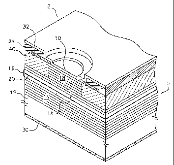
Referring to FIG. 1, a VCSEL 2 with variable tuning layer generally includes a
conventional VCSEL portion 5 and a variable tuning layer 10 having a thickness
predetermined in an intermediate process step to achieve a laser with a
desired slope
efficiency. Advantageously, the disclosed method can be used with virtually
any
conventional VCSEL design, an exemplary embodiment of which is described
herein.
The exemplary conventional VCSEL portion 5 includes a substrate 12, a first
or lower mirror 14, an optical cavity 16, and a second or upper mirror 18. The
substrate 12 is made of gallium arsenide (GaAs) or any other suitable
material. The
first and second mirrors are comprised of multilayered distributed Bragg
reflectors
(DBRs), as is conventional in the art. In the exemplary embodiment, aluminum
gallium arsenide (AlGaAs) with varying concentrations of aluminum and gallium
are
12
CA 02366583 2005-05-17
used to fabricate the mirrors. The optical thickness of each mirror layer is
typically
designed to be a quarter wavelength of the emitted light of the laser where
the optical
thickness is given by the product of the physical thickness and the index of
refraction.
The conventional optical cavity 16 (FIG. 1A) includes an active region 20
surrounded by first and second cladding regions 22, 24. The first and second
cladding
regions are made of AlGaAs in the exemplary embodiment. In the active region,
three
quantum wells 26 made of GaAs are disposed adjacent barrier layers 28 made of
A10.25Gao775As. As is generally understood, the number of and materials
forming the
quantum wells and surrounding barrier layers can be varied depending on the
design.
The epitaxial structure is preferably formed into discrete lasers by a
combination of current confinement and ohmic contacts. The contact
metalization
forming n-ohmic contact 30 on the bottom of the substrate may be, for example,
eutectic gold germanium deposited by electron beam evaporation or sputtering.
The
top contact metalization forming p-ohmic contact 32 may be, for example, gold
with
2% beryllium added or a layered structure of titanium/platinum/gold,
preferably
deposited by electron beam evaporation. Current constriction is preferably
provided
by using proton implantation region 40 to convert the upper mirror DBR 18 to
high
resistivity in all areas except the active device, isolating the devices into
individual
VCSELs while in wafer form. Other techniques for current constriction, such as
selective AlGaAs oxidation, are also applicable. A probe pad metalization 34
is
preferably disposed onto the p ohmic contact 32 to provide for wire bonding
and
electrical testing.
The variable tuning layer 10 is preferably disposed on the conventional
VCSEL structure 5 to tune the slope efficiency and thereby compensate for
manufacturing variations. The variable tuning layer may be made of any
optically
transparent, mechanically stable material. In a preferred embodiment, the
variable
tuning layer is formed of a dielectric layer of a silicon oxide or silicon
nitride, whose
thickness is chosen to center the slope efficiency distribution of the lasers
on a wafer
to compensate for wafer to wafer variation in the slope efficiency.
The thickness of the variable tuning layer 10 is preferably in the range from
about zero to about one quarter wavelength, or multiples thereof, for yielding
a final
surface reflection that can be continuously varied from in phase to out of
phase with
the adjacent DBR. The term "surface reflection" is meant to have an ordinary
meaning
13
CA 02366583 2005-05-17
as known in the art, and is further meant to cover any reflections on surfaces
(e.g., air,
plastic, or a plurality of layers comprising an additional Bragg reflector),
relating to a
top layer and/or one or more intermediate layers. In practice, the phases of
all
reflections above the variable tuning layers are changed relative to the
layers below
the variable tuning layer. In the preferred embodiment, the tuning layer 10
has the
effect of altering the top facet reflectivity of the VCSEL in a predictable
manner,
thereby adjusting the slope efficiency of the overall device, and enabling the
production of a plurality of lasers having consistent slope characteristics
from
different wafers.
Referring also to FIG. 2, the VCSEL 2 with variable tuning layer 10 is
preferably manufactured according to a process that includes the steps of
fabricating
42 the initial VCSEL portion; measuring 44 a characteristic of the initial
VCSEL
portion 5, such as its resistance or slope efficiency; determining 46 the
thickness of
the variable tuning layer 10 based on the measured characteristic necessary to
change
t5 the slope of the laser to a desired value; and depositing 47 a variable
tuning layer 10
having the determined thickness to produce a laser with the desired slope.
Each of the
steps is described in more detail hereinafter.
As shown in FIGS. 3 and 4, in the preferred embodiment, the VCSEL with
variable tuning layer is made by initially fabricating a wafer 50 of
conventional
VCSEL portions 5 leaving the surfaces of the VCSELs, which may include
dielectric
passivation layers, exposed. The various layers of the VCSELs are epitaxially
deposited on the semiconductor substrate following techniques well known in
the art.
One such technique is described in U.S. Patent No. 4,949,350. To facilitate
testing, a
probe pad 34 is placed on the devices on the wafer to make a contact for
electrical
testing and subsequent wire bonding of the completed lasers.
Once the conventional VCSEL portions 5 are fabricated, one or more
characteristics of the initial lasers, such as resistance or slope efficiency,
for example,
is measured directly or indirectly by any conventional method. In the
preferred
embodiment, the measuring step is carried out as shown in FIG. 5 by placing
the wafer
50 on a grounded chuck (not shown) of a conventional autoprober 54 which is
preferably modified by any suitable technique to include the disposition of a
broad
area photodetector 56 above the probe tip 58. The probe tip is then moved into
14
CA 02366583 2005-05-17
physical contact with probe pad 34 on the initial VCSEL portions 5, enabling
electrical testing.
The process of measuring the slope efficiency of the initial VCSELs 5 is
preferably performed by determining the ratio of the change in laser optical
output
power produced by a change in the input bias current. This can be
accomplished, for
example, by stepping the applied bias current while measuring the optical
output
power with the photodetector to generate a current to light characteristic
shown in box
60. In one method of calculation, the light characteristic is searched for the
low
current In,;I, that produces a specified low level optical power Pmin. The
high current loP
is then calculated by adding a specified modulation current Imod to Imin such
that:
(I) lop = Imi. + Imod
The corresponding high level optical power Pop is determined from the measured
characteristic, and the slope efficiency rjext is calculated by
(11) Tlext = (Pop-Pmin)/(Imod)
The low level power Pn,iõ and modulation current Imod are preferably chosen to
be
representative of the conditions used in the higher level assemblies. Other
conventional methods such as linear regression may be used to calculate slope
efficiency as is known in the art.
The measurement of slope efficiency is preferably made on a representative
sample of VCSELs to capture the slope efficiency distribution for the wafer.
For
example, in a typical VCSEL layout, some 20,000 devices may be formed on a
three
inch wafer. A representative sample may be on the order of 200 devices, for
example,
spatially distributed on a regular grid over the wafer surface.
Once the slope efficiency has been determined, the next step in the preferred
embodiment is to modify the optical efficiency of the laser in order to
achieve the
desired slope efficiency. The slope efficiency rlext of a laser is the product
of the
internal efficiency r1i and the optical efficiency rlopt
(III) 'qoPt = Tli 11opt
CA 02366583 2005-05-17
The internal efficiency rii is the fraction of electrons that are converted to
photons
while the optical efficiency rloPt is the fraction of photons that are
transmitted out of
the laser. As shown in equation (III), adjusting the optical efficiency rloPt
so that the
product is constant can compensate for variations in the internal efficiency.
The optical efficiency rloPt is calculated as the ratio of the transmission to
the
sum of the transmission and optical losses,
(IV) rlopt = T/(T + L)
where T is the transmission out of the cavity where the light is generated to
the output
facet, and L is the sum of all other losses including transmission out the
other side of
the laser.
In practice, the transmission is modified by the variable tuning layer which
alters the top facet reflectivity of the laser. Accordingly, the optical
efficiency, and
hence the slope, becomes adjusted. While the internal efficiency ordinarily
varies in
an unpredictable fashion, the change in transmission of the VCSEL as
additional
layers are deposited is highly predictable. Once the slope efficiency of the
VCSEL has
been measured, the internal efficiency for that wafer is essentially fixed, so
the
transmission can be tuned to compensate.
The thickness of the variable tuning layer 10 to achieve the desired slope is
preferably determined in the following manner. A ratio is first calculated
between the
measured slope efficiency to the desired value, and then a predetermined
lookup table,
described in more detail below, is referenced which relates the slope
efficiency ratio to
a tuning layer thickness. The desired values of slope efficiency for the
VCSELs may
be based, for example, on specifications for the VCSELs or specifications for,
or tests
conducted on, higher level assemblies.
Referring to FIGS. 5 and 6, once the variable tuning layer 10 is deposited
onto
the initial VCSEL 5, via holes 62 are preferably etched to the probe pad 34 to
provide
a contact for further electrical testing. The representative sample lasers are
preferably
retested to confirm the effectiveness of the variable tuning layer 10. The
tuning
process may then be repeated, if needed, taking into account the tuning layer
thickness
already on the wafer. In practice, the tuning during the first quarter
wavelength is
16
CA 02366583 2005-05-17
monotonic, and therefore error in thickness is made on the low side to enable
recovery
from deviations by additional deposition rather than etching, although etching
may be
used if needed. Furthermore, the yield is preferably optimized by centering
the wafer's
distribution within a specification, so the above process is preferably
applied to center
the distribution and maximize yield.
Referring to FIG. 8, the encapsulation medium matching layer 100 may be a
one half wavelength silicon nitride layer, followed by four alternating pairs
of one
quarter wavelength silicon oxide 102, 104, 106, 108 and silicon nitride layers
103,
105, 107, 109, configured as the additional DBR 80. As is conventional in the
art, the
layer thicknesses are computed using the wavelength as measured in the
material, so
that the nitride layers with a higher index of refraction have a smaller
absolute
thickness than the oxide layers with a lower index of refraction. The
thicknesses are
preferably chosen to ensure that all reflections add completely in-phase
relative to the
original VCSEL upper mirror 18 reflection. The dephasing (tuning) layer 86 is
a
variable-thickness oxide layer whose thickness is in the range of from about
zero to
about one quarter wavelength, or multiples thereof, to yield a final
reflection which
can be continuously varied from in phase to out of phase with the preceding
reflections. As the thickness of the layer increases from zero, the reflection
becomes
progressively more out of phase and the total transmission out of the VCSEL is
increased.
Referring to FIG. 9, the preferred process for fabricating VCSELs with
consistent slopes from a plurality of wafers is disclosed by graphical
illustration.
Through the measuring step, tests conducted on initial lasers from two
different
wafers prior to the tuning process show that the wafers have substantially
different
slope efficiency distributions centered as shown in curves 72 and 74. Both
distributions are preferably greater than the desired efficiency 76, which is
preferably
set at the center of the specified distribution. The presently preferred
process is to
deposit the four period DBR 80 (FIG. 8) over the upper mirror to reduce the
slope
efficiencies for the wafers below the specified range as shown in curves 82
and 84,
and then to deposit the wafer specific predetermined silicon dioxide tuning
layer 86
(FIG. 8) to tune the slope efficiencies for the lasers on each of the wafers
toward the
desired value as shown in curves 88 and 90. As shown in FIG. 9, the tuning
layer 86
increases the transmission until it reaches an optical thickness of one
quarter
17
CA 02366583 2005-05-17
wavelength, and then the transmission is reduced to a minimum at a thickness
of one
half wavelength. The tuning is thus cyclical with layer thickness, oscillating
with each
half wavelength deposition. In another embodiment, one could start with two
wafers
as represented by curves 82, 84 and then increase the transmission by applying
either
silicon oxide or silicon nitride tuning layers as shown in curves 88 and 90.
In practice, a look up table such as in Table I is used to determine the third
DBR stack and thickness of the variable tuning layer 86 to move the slope
efficiency
toward the center of the specification. As is shown in the "scaled" column,
the tuning
in the exemplary embodiment provides a 2x range (0.221/0.113) in the final
slope
efficiencies.
TABLE I
Exemplary Lookup Table for an 850 nm VCSEL
Including a Four Period Dielectric DBR and a Variable Oxide Tuning Layer
(calculated up to a quarter wave optical thickness)
VCL structure Oxide (D) rans ss rl opt scaled
Initial no mirror 0.256 0.3 .461 1.000
4 periods + .017 .3 .052 .113
4 periods + 200 .017 .3 .053 v.115
4 periods + 400 0.018 0.056 0.122
4 periods + 600 0.020 0.3 .063 0.136
4 periods + 800 .023 0.3 .071 .155
4 periods + 1000 .027 0.3 0.083 0.180
4 periods + 1200 .032 0.3 0.096 .209
periods + 1400 p.034 .3 .102 .221
The ratio of the center of the specified distribution to the median of the
measured slope efficiency distribution is referred to in the "scaled" column
of Table 1.
The corresponding value for the oxide tuning layer thickness is then selected
from the
"oxide" column of Table 1. For example, if a slope efficiency distribution of
an initial
VCSEL wafer is centered on a value of 0.44mW/mA, and the desired center for
the
distribution is 0.06mW/mA, then the ratio is 0.06/0.44 = 0.136 and the oxide
18
CA 02366583 2005-05-17
thickness to be deposited is preferably 600 angstroms, according to the
exemplary
table.
In the preferred embodiment, the additional Bragg stack 80 and tuning layer 86
are deposited using plasma enhanced chemical vapor deposition. As is
conventional in
the art, such optically transparent films can be routinely deposited in
increments
below 50 angstroms. In addition, an adhesion layer, such as titanium, is
preferably
deposited onto any exposed gold surfaces prior to dielectric deposition to
enable good
mechanical stability of the dielectric mirror and tuning layer. The titanium
layer,
typically on the order of a 100 angstroms thick, may be deposited by any
suitable
method, such as by sputtering or electron beam evaporation. Once the
dielectric mirror
and tuning layer have been deposited, the film is preferably patterned and
etched to
create via holes (e.g., 62, FIGS. 6 and 7) for electrical contact. The
patterning and via
etching may be accomplished using conventional photolithography techniques to
mask the films and plasma etching using any suitable reactive gas such as
CF4/02.
With the additional mirror and tuning layer complete, the lasers may be
retested, if
desired, by any suitable method to confirm that the process achieved the
desired
result.
The lookup table may be determined by calculation, empirical data, or any
other suitable method. To determine the table empirically, any suitable
procedure may
be used. In practice of a presently preferred method, a conventional VCSEL
wafer is
processed to a testable level, and a representative sample of lasers is tested
to
determine the slope efficiency. Subsequently, a third mirror comprising any
desired
number of DBRs (including none) is deposited, followed by a partial deposition
of the
tuning layer. Vias are etched in the dielectric tuning layer to enable
testing, and the
same sample is retested. The procedure is preferably repeated until a complete
quarter-wave thickness of tuning layer has been deposited. The data for the
median
device provides a table of slope efficiency vs. tuning layer thickness for the
device.
Normalizing the slope efficiency data by the initial value produces the
"scaled"
column in Table 1.
Alternatively, to determine the table by calculation, the transmission from
the
cavity out of the VCSEL surface can be calculated using conventional
transmission
matrices, such as those generally described in Scott, J.W., "Design,
Fabrication and
Characterization of High-Speed Intra-Cavity Contacted Vertical-Cavity Lasers",
19
CA 02366583 2005-05-17
University of California, Santa Barbara, Electrical and Computer Engineering
Technical Report #95-06, or by any other suitable technique known in the art.
The
calculation is applied to various tuning layer thicknesses, producing the data
in the "T"
column of Table 1.
In the exemplary table set forth above, the power transmission T and round
trip optical loss L are expressed in percent. The transmission is the fraction
of power
transmitted out of the cavity on a single reflection, while the optical loss
represents the
fractional power loss as a wave makes one complete round trip propagation
within the
cavity. The optical loss is a combination of internal losses that arise
predominantly
from free carrier absorption as well as transmission out the lower mirror DBR
stack.
In exemplary Table 1, the optical loss L is presumed constant wafer to wafer
and
generally remains constant for a given wafer. It can also be estimated using
the
transmission matrix formalism, or can be determined experimentally by
correlating a
set of experimental slope efficiency measurements with the theoretical
prediction.
Once the transmission T and optical loss L have been determined, the values
for the
optical efficiency n opt are calculated using equation N. To produce the
scaled data,
the values of rloPt are normalized to the initial riopt value.
A second order effect that may be taken into account is that the transmission
out of the lower mirror varies depending on the accuracy of the VCSEL growth
relative to the design. These variations can usually be ignored, but may be
important
to consider if the growth thickness accuracy is highly variable, which may
occur in
some VCSEL manufacturing processes. In this case, a refinement of the
described
tuning process preferably includes modification of the optical loss values.
The optical
loss values to be used may be correlated with spectral measurements of the
initial
VCSEL or dynamic fits of optical loss value to agree with the change in slope
observed upon the application of an intermediate dielectric deposition and
test step.
FIG. 10 illustrates the VCSEL 2 with variable tuning layer 10 mounted into an
optical subassembly (OSA) 110. The OSA 110 enables application of DC biasing
and
AC modulation signals to the VCSEL 2. With the exception of the VCSEL 2, all
of
the parts of the OSA are conventional. The OSA generally comprises an
electrical
package 112 containing the VCSEL 2 and a power monitoring photodetector 114.
The
electrical package is preferably bonded to a precision molded plastic housing
116. The
bonding process including conventional bonding material 117 preferably
involves
CA 02366583 2005-05-17
active alignment to optimize the coupling of the laser light into an optical
fiber 120, as
is conventional in the art. The OSA includes a ball lens 122 for coupling the
light into
the optical fiber. A ferule portion 134 of the housing 116 cooperates with the
fiber
assembly 124 to provide alignment of the optical fiber 120. After the
electrical
package 112 and housing 116 are bonded together, the fiber is removed and the
OSA
110 is complete.
By obtaining a more accurate slope for the VCSEL 2, more toleration for
mechanical variances in the OSA 110, and in the higher level assemblies is
permissible. These mechanical variances may include, for example, variations
in
concentricity from fiber to fiber, sub optimal active alignment variations,
shifts in
mechanical position due to environmental changes such as temperature, and
normal
connector tolerances to allow insertion of a fiber into the housing. Allowing
increased
mechanical variation reduces manufacturing complexity and increases yield,
thereby
resulting in lower overall product cost. Alternatively, the mechanical
tolerances may
be maintained at current levels to yield an OSA with more consistent
performance
characteristics.
FIG. 11 illustrates in block diagram form an optical transceiver 130
incorporating a VCSEL 2 with variable tuning layer fabricated according to the
inventive method. With the exception of the VCSEL 2, all of the parts of the
optical
transceiver are conventional. The transceiver includes a transmitter portion
131 and a
receiver portion 144. The transmitter portion provides an interface between a
differential input 133 and an optical fiber output. In operation, a
differential input
signal is converted to a single ended signal by emitter coupled logic (ECL)
line
receiver 137 and an AC modulation signal is applied to the single ended signal
in laser
driver 138. A DC bias signal is then applied to the signal by DC laser bias
signal
generator 139 for application to the OSA 110. Start up circuitry 140 and reset
circuitry
141 is preferably provided to control the transmission of data over the
optical fiber. A
laser fault indicator 145 provides a status indication of the transmitter
portion 131.
The receiver portion 144 takes an input from an optical fiber provided through
a photodetector 145 and converts it to a differential output signal. The
receiver pre
amp signal is preferably low pass filtered in filter 147 to remove any high
frequency
21
CA 02366583 2005-05-17
noise present, amplified in amplifier 148 to regenerate the digital signal,
and then
transmitted off the board through the differential output 146.
The use of VCSELs with highly consistent slopes in optical transceivers
enhances the performance and reliability of the data communications system.
This is
because the total optical subassembly slope variation can be effectively tuned
to fall
within specification, so the drive circuit will not have to be used to
compensate. Such
a system will not suffer from changes in high speed performance, and will
therefore
have the desirable effect of generally improving overall product consistency
and yield.
The VCSEL described above, or other optoelectronic component, may be
encapsulated in plastic, epoxy or other suitable encapsulant. The primary
benefits of
such a package are cost and manufacturability, which may be superior to the
conventional metal package. The encapsulation should preferably be optical
grade
plastic suitable for encapsulating a laser and other semiconductor components
while
also allowing transmission of light. One suitable plastic is sold by Dexter
Electronic
Materials Division, Industry, California, under the trademark HYSOL .
The plastic encapsulation package preferably contains a tilted window
beamsplitter for obtaining accurate monitoring and feedback as previously
described.
The beamsplitter window may be formed of an air gap, glass, plastic or
adjacent
media of differing indices of refraction, and may be fabricated in a number of
ways.
The various embodiments take into account the differing indices of refraction
to
provide the proper feedback of radiated light toward the photodiode. In
addition, the
geometries are preferably chosen to ensure a consistent sampling of the beam
at both
high and low beam divergence which may result from different drive currents
and
temperatures. The disclosed embodiments also serve to reduce inaccuracy in
monitoring and feedback due to modal variations in the radiated beam.
Referring to FIG. 12, the plastic encapsulation package 200 has substantially
the same dimensions as the conventional metal package 109 used in the optical
subassembly 110 of FIG. 10. This embodiment has the advantage of allowing
replacement of the package in the subassembly without significantly impacting
other
aspects of the subassembly. The encapsulation substantially encapsulates a
VCSEL
die 202 and a photodiode 206 which may be mounted on a conductive or
insulative
stand 204 for electrical or thermal dissipation considerations.
22
CA 02366583 2005-05-17
The package preferably includes a base portion 208 that replaces the standoff
112 (FIG. 10) in the optical subassembly, and a cylindrical body portion 210
which is
formed by the encapsulation material. The top 212 of the body portion
preferably
contains a recess 214 containing a ledge 216. The ledge is positioned to house
a tilted
window beamsplitter 218 in optical alignment with the VCSEL for reflecting a
portion
of the radiated light toward the photodiode 206. The window is preferably
glass. The
index of refraction of the glass, in conjunction with the indices of
refraction of air
gaps 215 in the recess and the plastic encapsulation, provides the necessary
refraction
to appropriately direct a representative sample of the radiated beam onto the
photodetector while transmitting an undistorted beam into the output.
Referring to FIG. 13, the above power monitoring arrangement may be
incorporated into a plastic system of lenses to provide transmit/receive
functions. One
method of construction, known as the small form factor (SMFF) package 300,
encapsulates the laser 301 and receiver 302 in plastic, and then aligns and
attaches a
plastic lens/fiber connector piece 303 onto the encapsulated devices. The
benefit of
this approach is that the plastic encapsulation may be performed with
mechanical
tolerances typical of the technology, on the order of 25 to 50 microns. The
precise
alignment to < 5 m of the fiber and lens to the devices is achieved during a
subsequent alignment step, effectively decoupling the two technologies. For
such
applications the alignment may be done using active electrooptic measurements
or
with vision aided alignment. The advantage of a vision system is that the
alignment
may be done in an automated fashion, stepping from device to device on a
regular
pattern on a leadframe. This cassette driven approach may provide
substantially higher
throughput on the equipment, reducing overall cost.
Referring to FIG. 14, another plastic molded package 400 (index nl) (nl)
encapsulates the VCSEL die 402, photodiode 404 and substrate 406. The
substrate
406 may be any material suitable for the attachment of semiconductor die, such
as a
metal leadframe, a ceramic substrate, or a standard printed circuit board
epoxy/glass
laminate. In the preferred embodiment, a tilted window 408, preferably made of
glass
3o having an index of refraction (n2), is coupled to the plastic molded
package 300. The
tilted window 408 is preferably coated with a 1/4 wave reflective coating 410,
having
an index of refraction (n3) that may be tailored to obtain optimal monitoring
23
CA 02366583 2005-05-17
and feedback. In the preferred embodiment, an optically clear epoxy 412 with a
refractive index (n4), that substantially matches the refractive index nl of
the plastic
molded package 400, couples the tilted window 408 to the plastic molded
package
400. The reflectance of the tilted window and quarter wave coating may be
adjusted
by adjusting the index ratio n2/n3.
In this embodiment, the index of refraction of the quarter wave coating 410 is
preferably higher than the refractive index (nl) of the plastic molded package
400.
Preferably, the refractive index of the plastic molded package, (nl) and the
refractive
index of the tilted window n2, are comparable. Therefore, the power reflected
at the
interface of the tilted window 408 and the plastic molded package 400, given
by the
square of the ratio (nl-n2)/(nl+n2), is relatively small. In the preferred
embodiment,
the refractive index n3 of the quarter wave reflective coating 410 may be
tailored to
significantly reflect incident light utilizing readily implemented
manufacturing
processes.
For example, if the refractive index of the plastic molded package nl is 1.5
and the tilted window 408 has a refractive index n2 of 1.45, the net
reflection at the
interface of the plastic molded package and the tilted window would be
approximately
0.03%. However, treating the tilted window 408 with a quarter wavelength thick
layer
of silicon nitride, with a refractive index n3 of 2.0, increases the reflected
power to
9%. Advantageously, the silicon nitride may be uniformly and precisely
deposited
using conventional techniques such as plasma enhanced chemical vapor
deposition.
The quarter wave reflective coating 310 should preferably be uniform to avoid
distorting the beam. In addition, the optimum quarter wave thickness may be
effectively realized in conjunction with multiple half wavelength deposits of
the
coating as may be desirable from a manufacturing perspective, (thickness =
1/41 +
nl/2, where n is an integer).
A glass or plastic triangular shaped plastic piece 414 may be coupled to the
top
surface of the tilted window 408 using an optically transparent epoxy 412 with
a
refractive index (n4) which substantially matches the refractive index of the
tilted
window (n2). A lens 416 is preferably housed in a conventional lens barrel
418. The
fiber 420 is aligned above the lens barre1418.
24
CA 02366583 2005-05-17
As an alternative to applying a 1/4 wave reflective material such as silicon
nitride on the tilted window 408, a thin metallic coating on the window may
also be
utilized to control the power level of light reflected from the tilted window
408. For
example, a layered coating of titanium and gold may be used to reflect a small
percentage of the beam while transmitting the majority of the beam through the
coating. An alternate embodiment includes a titanium layer in the range 20 to
50
Angstroms, deposited directly on the tilted window 408, followed by a 100 to
200
Angstrom layer of gold deposited on the layer of titanium.
Referring to FIG. 15, the optoelectronic device 440 may alternatively be
encapsulated in an optically transparent epoxy 442 such as is used in direct
butt-coupling to a fiber 444. The optoelectronic device is connected to a
substrate 448
through a conventional wire bond 450. In a butt-coupling approach, the fiber
444 is
epoxied directly to the device surface 452 with the optically transparent
epoxy 442
filling the minor gap 456. Additional mechanically stable epoxy 458 may be
used for
further support. This simple approach is highly desirable as it removes the
need for
any optical elements. The fiber 444 can be placed vertical to the surface 452,
as
shown, or parallel with a 450 metallized facet positioned to reflect the light
down the
fiber. Many other configurations fall within the scope of the invention, the
critical step
being the change of the material on the surface of the optoelectronic device.
The present invention includes as a particularly preferred embodiment, a
design for an optoelectronic component, such as a VCSEL, LED or resonant
cavity
photodetector (RCP), whose transmission does not change upon encapsulation by
a
material with a known index of refraction. The optoelectronic component may be
encapsulated in any suitable manner, including in any one of the plastic
encapsulation
or epoxy encapsulation approaches as set forth above.
In practice, the surface reflection of the optoelectronic component typically
is
very different depending on whether it is terminated in air or the
encapsulant, with a
much larger reflection in the case of air. It is known that the surface
reflection can be
made out of phase with the rest of the mirror, effectively increasing the
transmission.
The amount of the transmission increase can be adjusted by controlling the
thickness
of the surface layer. Once the VCSEL is encapsulated, the surface reflection
is
reduced, and the transmission at the facet is increased but the dephased
reflection is
also reduced. By adjusting the surface layer thickness correctly, the overall
CA 02366583 2005-05-17
transmission from the laser into the terminating material is unchanged, be it
air or
encapsulation. As a result, the laser properties such as slope efficiency and
threshold
current are unchanged upon encapsulation.
Distributed Bragg reflectors are generally used by those skilled in the art to
create the optical feedback required for VCSEL lasing action. The facet of the
laser is
therefore completed with a material, typically semiconductor or silicon
nitride, in
contact with air of vacuum. The field reflection coefficient, r12 as a wave
traveling in
material 1 strikes the interface with material 2 is given by:
io (1) r12 = (nl - n2)/(nl + n2)
where nl the index of refraction in material I and n2 is the index of
refraction in
material 2. The power reflection coefficient is given by
(2) R12 = r12 r12
where r12 is the complex conjugate off r12 If the final material is changed
from air to
plastic, for example, 112 changes from I to 1.5 respectively. If the initial
material is
GaAs, with an index '9l of 3.5, the power reflection changes from 0.31 to 0.16
respectively. If some special technique is not employed, the transmission out
of the
laser will be substantially changed upon encapsulation.
The slope of a laser, rleX1 is generally describe as the product of the
internal
efficiency ni and the optical efficiency %,pt
(3) '9ext = Tli TIopt
The internal efficiency is the fraction of electrons that are converted to
photons while
the optical efficiency is the fraction of photons that are transmitted out of
the laser.
Variations in the doping, current confinement and active region properties all
effect
the internal efficiency. The optical efficiency is calculated as the ratio of
the
transmission to the sum of the transmission and optical losses,
26
CA 02366583 2005-05-17
(4) rlopt = T
T+L
where T is the transmission out of the cavity where the light is generated to
the output
facet and L is the sum of all other losses including transmission out the
other side of
the laser. The transmission and losses can be calculated as described in
detail in the
Ph. D dissertation, "Design, Fabrication and Characterization of High-Speed
Intra-Cavity Contacted Vertical-Cavity Lasers," University of California,
Santa
Barbara, Electrical and Computer Engineering Technical Report #95-06, June
1995.
The threshold current of a semiconductor diode laser is the amount of
electrical
current that must be supplied to sustain the population inversion that is
required to
provide the threshold optical gain, Gh The threshold optical gain is given by
(5) Gth = T+ L
It is therefore clear that substantial changes in transmission will have
significant
effects on the laser slope and threshold current.
If an encapsulation medium matching material (medium matching), whose
index of refraction is similar to the encapsulant, is disposed on top of the
laser as a
part of a dielectric mirror, its surface reflection will, essentially vanish
upon
encapsulation. Optically, it is part of the encapsulation. For example,
silicon dioxide,
Si02, has an index of refraction of 1.45. The power reflectivity for
termination with
air is 3% but drops to 0.03% when terminated by an index of 1.5. Oxynitride,
SiNXOy,
can be used as a medium matching material whose index can be controlled
between
1.45 and 2 for a better match with the encapsulant.
Referring to FIG. 16, in one embodiment of the invention, the method involves
fabricating the initial optoelectronic device (step 500), measuring a
characteristic of
the device (step 502), determining the thickness of a medium matching layer
needed
to maintain the characteristic substantially the same post-encapsulation (step
504),
depositing the medium matching layer with the desired thickness (step 506),
and
completing the processing (e.g., testing), packaging and encapsulation of the
device
(step 508).
27
CA 02366583 2005-05-17
For a VCSEL, the design procedure is as follows. The transmission from the
VCSEL cavity out of the top facet into the encapsulating index is calculated
without
the medium matching layer. Then the transmission is calculated with
termination in
air with the medium matching layer whose index matches the encapsulant. The
thickness of the medium matching layer is adjusted until the transmissions are
the
same.
In a presently preferred embodiment, the process includes growing a VCSEL
wafer, fabricating it into lasers, and then depositing a dielectric
distributed Bragg
reflector. The materials used are typically silicon nitride, Si3N4 and silicon
oxide,
Si02, which are transparent to the wavelengths of our lasers and can easily be
deposited using plasma enhanced chemical vapor deposition. Layer thickness is
specified in terms of optical wavelengths as is standard in the art.
The transmission of the mirror is calculated for termination on both air (n =
1)
and plastic (n = 1.5) using the transmission matrix formalism. The results at
850nm,
the design wavelength in this example, are given in the table of FIG. 17. As
shown in
the table, at a thickness of 840 angstroms, an medium phase matching layer
provides
the same transmission and hence laser properties regardless of whether the
laser facet
is terminated in air or plastic.
The medium matching layer described herein can be combined with the
previously disclosed tuning layer process, disclosed in detail above, which
adjusts the
laser slope based on test data of the "as grown" VCSEL to provide consistent
slope
efficiencies. In the case of the desire to provide both encapsulation medium
matching
and slope tuning, one of the layers in the lower dielectric mirror can be
tuned while
the top medium matching layer is designed to ensure unchanging slope upon
encapsulation. For example, referring to FIG. 18, a layer 1 is a silicon oxide
medium
matching layer while the silicon nitride mirror layer 8 can be utilized as the
tuning
layer. Because the distributed Bragg reflector is a coupled system of
reflections, the
two cannot be optimized independently but can be easily designed using the
transmission matrix formalism, the results of an example are shown in FIG. 19.
The
transmission is matched for both air (n=1) or plastic (n = 1.5). The nitride
has an index
of refraction of 2. A quarter optical wave at 850nm is given by 8500/(4*2) =
1062
angstroms. We therefore start with 1062 angstroms and can either increase or
decrease
its thickness, as the tuning is periodic with every half wave or 2125
angstroms. Using
28
CA 02366583 2005-05-17
the modified table shown in FIG. 19, all the tuning layer processes previously
disclosed are applicable.
Accordingly, the non-quarter wave layer is disposed whose thickness and
surface reflection create the same transmission as when the material is
embedded in a
material whose index is similar to the medium matching layer, effectively
eliminating
the dephased surface reflection. The medium matching layer can be any number
of
materials transparent to the light whose index is similar to the encapsulant.
The use of
four periods of oxide/nitride layers is not essential to the invention. It
would be
possible to use any number of layer combinations; it is the design for
substantially
t0 identical transmission in air or encapsulant that is unique.
Referring to FIG. 20, the steps of this process therefore include fabricating
the
initial VCSELs (step 542), measuring the slope efficiency of the VCSELs (step
544),
determining the thicknesses of the tuning layer and medium matching layer to
achieve
the desired slope efficiency (step 546), depositing the tuning layer and
medium
matching layer as indicated above having the determined thicknesses (step
547),
measuring/confirming the slope (step 548), and processing, packaging and
encapsulating the VCSELs (step 550).
An advantage of this invention is that the test data taken while the die are
still
in wafer form remain unchanged when the lasers are encapsulated. Wafer level
testing
is the lowest cost approach and allows the selection of only "known good die"
to enter
the value added packaging processes. Without this invention, careful
correlation of
performance data, before and after encapsulation, would have to be used to set
wafer-level specifications, along with additional testing requirements of
packed lasers
that can be eliminated by the use of this invention to enable accurate testing
at the
wafer level. For example, measuring the temperature performance of the lasers
to
enable determination of optimum current operation over temperature is an
effective
manufacturing solution that becomes much more difficult once the laser
properties
change upon ncapsulation of epoxy assembly. Many other applications for VCSELs
beyond communications will also benefit from laser properties that remain
unchanged
upon encapsulation. For example, sensing application may use encapsulated
VCSELs
where the laser properties need to be well controlled.
Those skilled in the art will understand that various modifications can be
made
to the present invention without departing from its spirit and scope. For
example, the
29
CA 02366583 2005-05-17
teachings of this invention may readily be applied to other types of
optoelectronic
components, such as LEDs or resonant cavity photodetectors.