Note : Les descriptions sont présentées dans la langue officielle dans laquelle elles ont été soumises.
CA 02368141 2001-09-17
WO 00/69028 PCT/EP00/03992
1
Beschreibung
Leiterplatten-Steckverbinder
Die vorliegende Erfindung betrifft eine Vorrichtung gemaf~ dem
Oberbegriff des Patentanspruchs 1, d.h. einen Leiterplatten-
Steckverbinder zum Verbinden einer ersten Leiterplatte and
einer im wesentlichen senkrecht auf diese aufsteckbaren zwei-
ten Leiterplatte, wobei der Leiterplatten-Steckverbinder auf
der ersten Leiterplatte montiert ist, and wobei der Leiter-
platten-Steckverbinder derart ausgebildet ist, dai3 er mit auf
gegeniiberliegenden Seiten der zweiten Leiterplatte vorgesehe-
nen elektrischen Verbindern in Kontakt bringbar ist.
Leiterplatten-Steckverbinder, die dazu ausgelegt sind, mit
auf gegenizberliegenden Seiten einer Leiterplatte vorgesehenen
elektrischen Verbindern in Kontakt gebracht zu warden, sind
erforderlich, wail die Anzahl der Kontakte, die Leiterplat-
ten-Steckverbinder aufweisen mussen, immer waiter steigt;
fiber beiderseits einer Leiterplatte vorgesehene elektrische
Verbinder konnen - bezogen auf die Lange der elektrischen
Verbinder (der Leiterplatte) - mehr Kontakte untergebracht
warden als wenn nur auf einer Seite der Leiterplatte ein
elektrischer Verbinder vorgesehen ware.
Die Herstellung derartiger Leiterplatten-Steckverbinder er-
fordert wegen der sehr groi3en Anzahl von in der Regal sehr
dicht angeordneten Kontakten, fiber welche sie mit darauf auf-
zusteckenden Leiterplatten and mit der sie tragenden Leiter-
platte in Verbindung zu bringen sind, hochste Prazision. Dies
gilt in besonderem Mane, wenn die Verbindung zwischen dam
Leiterplatten-Steckverbinder and der diesen tragenden Leiter-
platte nach einem SMT-Verfahren erfolgt (der Leiterplatten-
Steckverbinder ein oberflachenmontierbarer Leiterplatten-
Steckverbinder ist). Entsprechendes gilt fur die auf den Lei-
terplatten-Steckverbinder aufzusteckende Leiterplatte and die
Montage der auf dieser vorgesehenen elektrischen Verbinder.
ERZSATZBLATT (REGEL 26)
CA 02368141 2001-09-17
WO 00/69028 PCT/EP00/03992
2
Unabhangig davon Bind Leiterplatten-Steckverbinder der ein-
gangs genannten Art auch nur sehr schwer handhabbar.
Der vorliegenden Erfindung liegt daher die Aufgabe zugrunde,
den Leiterplatten-Steckverbinder gemai~ dem Oberbegriff des
Patentanspruchs 1 derart weiterzubilden, daf3 dieser auch bei
hochsten Qualitats- and Zuverlassigkeitsanforderungen relativ
einfach herstellbar and handhabbar ist.
Diese Aufgabe wird erfindungsgemai~ durch das im kennzeichnen-
den Teil des Patentanspruchs 1 beanspruchte Merkmal gelost.
Demnach ist vorgesehen, dai3 der Teil des Leiterplatten-
Steckverbinders, der mit dem auf der einen Seite der zweiten
Leiterplatte vorgesehenen elektrischen Verbinder in Verbin-
dung zu bringen ist, and der Teil des Leiterplatten-
Steckverbinders, der mit dem auf der anderen Seite der zwei-
ten Leiterplatte vorgesehenen elektrischen Verbinder in Ver-
bindung zu bringen ist, durch separate elektrische Verbinder
gebildet werden.
Eine derartige Aufteilung des Leiterplatten-Steckverbinders
in mehrere separate Teileinheiten erweist sich gleich in
mehrfacher Hinsicht als vorteilhaft: Einerseits lassen sich
dadurch geforderte Toleranzen (beispielsweise die bei SMT-
Verfahren geforderte Koplanaritat der Anschlusse) leichter
einhalten, andererseits konnen veranderliche Parameter (bei-
spielsweise unterschiedliche Dicken der auf den Leiterplat-
ten-Steckverbinder aufzusteckenden Leiterplatte) mit geringe-
rem Aufwand berucksichtigt werden, and schlief~lich lassen
sick die kleineren Teileinheiten (beispielsweise von Bestiik-
kungsautomaten) leichter handhaben.
Der beanspruchte Leiterplatten-Steckverbinder ist damit auch
bei hochsten Qualitats- and Zuverlassigkeitsanforderungen re-
lativ einfach herstellbar and handhabbar.
ERZSATZBLATT (REGEL 26)
CA 02368141 2001-09-17
WO 00/69028 PCT/EP00/03992
3
Vorteilhafte Weiterbildungen der Erfindung sind den Unteran-
spriichen, der folgenden Beschreibung and den Figuren entnehm-
bar.
Die Erfindung wird nachfolgend anhand von Ausfiihrungsbeispie-
len unter Bezugnahme auf die Figuren naher beschrieben. Von
den Figuren zeigen
Figur 1 eine perspektivische Ansicht einer Anordnung, in wel-
cher zwei Leiterplatten fiber den nachfolgend naher
beschriebenen Leiterplatten-Steckverbinder miteinan-
der verbunden sind, and
Figur 2 eine perspektivische Ansicht einer der Teileinheiten,
aus welcher der Leiterplatten-Steckverbinder gemal3
Figur 1 besteht.
Der nachfolgend naher beschriebene Leiterplatten-
Steckverbinder dient zur Verbindung einer ersten Leiterplatte
and einer senkrecht auf diese aufsteckbare zweite Leiterplat-
te.
Die erste Leiterplatte ist beispielsweise eine sogenannte
Ruckwandleiterplatte oder - allgemeiner ausgedriickt - ein
Baugruppentrager; die zweite Leiterplatte ist beispielsweise
eine auf eine Ruckwandleiterplatte aufzusteckende Einsteck-
karte oder - allgemeiner ausgedriickt - eine auf einen Bau-
gruppentrager aufzusteckende Baugruppe.
Der betrachtete Leiterplatten-Steckverbinder ist auf der er-
sten Leiterplatte montiert and dazu ausgelegt, mit auf gegen-
iiberliegenden Seiten der zweiten Leiterplatte vorgesehenen
elektrischen Verbindern in Kontakt zu kommen.
Der Zustand, im welchem die erste Leiterplatte and die zweite
Leiterplatte izber einen solchen Leiterplatten-Steckverbinder
ERZSATZBLATT (REGEL 26)
CA 02368141 2001-09-17
WO 00/69028 PCT/EP00/03992
4
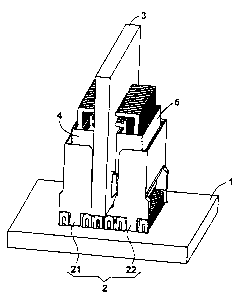
verbunden sind, ist in Figur 1 dargestellt. Dabei sind die
erste Leiterplatte mit dem Bezugszeichen 1, der darauf mon-
tierte Leiterplatten-Steckverbinder mit dem Bezugszeichen 2,
die zweite Leiterplatte mit dem Bezugszeichen 3, and die auf
dieser vorgesehenen elektrischen Verbinder mit den Bezugszei-
chen 4 and 5 bezeichnet.
Der Leiterplatten-Steckverbinder 2 zeichnet sich dadurch aus,
dai3 er aus mehreren separaten Teileinheiten besteht. Bei den
separaten Teileinheiten handelt es sich um separate elektri-
sche Verbinder 21 and 22, von welchen einer (der elektrische
Verbinder 21) dazu ausgelegt ist, mit dem auf der einen Seite
der zweiten Leiterplatte 3 vorgesehenen elektrischen Verbin-
der (dem elektrischen Verbinder 4) in Kontakt gebracht zu
werden, and von welchen der andere (der elektrische Verbinder
22) dazu ausgelegt ist, mit dem auf der anderen Seite der
zweiten Leiterplatte 3 vorgesehenen elektrischen Verbinder
(dem elektrischen Verbinder 5) in Kontakt gebracht zu werden.
Diese elektrischen Verbinder 21 and 22 sind separate Einzel-
teile, die unabhangig voneinander auf der ersten Leiterplatte
1 montierbar sind.
Die elektrischen Verbinder 21, 22 weisen im betrachteten Bei-
spiel einen identischen Aufbau auf and sind einander um 180°
gedreht gegeniibergestellt.
Einer der elektrischen Verbinder 21, 22, ist in der Figur 2
dargestellt.
Die elektrischen Verbinder 21, 22 bestehen aus einem Gehause
211, ersten Kontaktelementen 212 zur Verbindung derselben mit
der ersten Leiterplatte 1, and zweiten Kontaktelementen 213
zur Verbindung derselben mit den elektrischen Verbindern 4, 5
der zweiten Leiterplatte 3.
Die elektrischen Verbinder 21, 22 Bind im betrachteten Bei-
spiel oberflachenmontierbare Verbinder. D.h., die ersten Kon-
ERZSATZBLATT (REGEL 26)
CA 02368141 2001-09-17
WO 00/69028 PCT/EP00/03992
taktelemente 212 sind dazu ausgelegt, unter Verwendung eines
SMT-Verfahrens mit der ersten Leiterplatte verbunden (verlo-
tet) zu werden. Es sei jedoch bereits an dieser Stelle darauf
hingewiesen, daft hierauf keine Einschrankung besteht. Die
5 Verbindung zwischen den elektrischen Verbindern 21, 22 and
der ersten Leiterplatte kann auch auf beliebige andere Art
and Weise erfolgen.
Bei den zweiten Kontaktelementen 213 handelt es sich um in
zwei nebeneinander liegenden Reihen angeordnete Kontaktmes-
ser. D.h., die elektrischen Verbinder 21, 22 sind zweireihige
Messerleisten. Dementsprechend handelt es sich bei den elek-
trischen Verbindern 4, 5 der zweiten Leiterplatte 3 um zwei-
reihige Federleisten. Auch hierauf besteht jedoch keine Ein-
schrankung. Die zweiten Kontaktelemente 213 der elektrischen
Verbinder 21, 22 konnen auch beliebig anders beschaffen and
angeordnet sein.
Die elektrischen Verbinder 21, 22 nach Art der Figur 2 konnen
unabhangig voneinander auf die erste Leiterplatte montiert
werden. Insbesondere ist es problemlos moglich, den Abstand
zu variieren, in welchem sie parallel zueinander angeordnet
werden. Dadurch kann der Leiterplatten-Steckverbinder 2 der
ersten Leiterplatte 1 denkbar einfach an die jeweilige Dicke
der zweiten Leiterplatte 3 angepaf3t werden. Zur P.npassung des
Leiterplatten-Steckverbinders 2 an die Dicke der zweiten Lei-
terplatte 3 mussen nur die Lotpads, an welchen die ersten
Kontaktelemente 212 der elektrischen Verbinder angelotet wer-
den, entsprechend positioniert werden. Ware der Leiterplat-
ten-Steckverbinder wie bisher als eine zusammenhangende (ein-
teilige) Einheit ausgebildet, miif3ten fur verschiedene Dicken
der zweiten Leiterplatte 3 jeweils verschiedene Leiterplat-
ten-Steckverbinder bereitgestellt werden.
Die Aufteilung des Leiterplatten-Steckverbinders in separate
Teileinheiten erweist sich aber auch in anderer Hinsicht als
vorteilhaft.
ERZSATZBLATT (REGEL 26)
CA 02368141 2001-09-17
WO 00/69028 PCT/EP00/03992
6
Die Teileinheiten, genauer gesagt die elektrischen Verbinder
21, 22 weisen jeweils eine geringere Anzahl von Kontaktele-
menten (im betrachteten Beispiel jeweils nur halb so viele
Kontaktelemente) auf als der Leiterplatten-Steckverbinder 2.
Dies erweist sich insbesondere bei den ersten Kontaktelemen-
ten 212 als Vorteil. Diese lassen sich (wegen deren ver-
gleichsweise geringen Anzahl) mit verhaltnismai3ig geringem
Aufwand koplanar ausrichten, was bei Verwendung von SMT-
Verfahren zur Verbindung mit der ersten Leiterplatte 1 von
groi~ter Bedeutung ist; die Anschliisse von unter Verwendung
eines SMT-Verfahrens zu montierenden Bauteilen mussen be-
kanntlich koplanar ausgerichtet sein.
Abgesehen davon lassen sich die separaten Teileinheiten der
Leiterplatten-Steckverbinders wegen deren vergleichsweise ge-
ringen Groi~e (beispielsweise von Bestiickungsautomaten) erheb-
lich einfacher handhaben als ein als eine zusammenhangende
Einheit ausgebildeter Leiterplatten-Steckverbinder.
Im betrachteten Beispiel handelt es sich bei den Teileinhei-
ten (den elektrischen Verbindern 21, 22) des Leiterplatten-
Steckverbinders um identisch ausgebildete Komponenten. Dies
erweist sich zwar als besonders vorteilhaft, well dann nur
eine minimale Anzahl verschiedenartiger Teile hergestellt and
montiert werden mui3, ist aber nicht zwingend erforderlich.
Bei den elektrischen Verbindern 21, 22 kann es sich auch um
verschiedene elektrische Verbinder handeln. Beispielsweise
kann der erste elektrische Verbinder 21 eine zweireihige Mes-
serleiste sein, and der zweite elektrische Verbinder eine
vierreihige Messerleiste.
Der beschriebene Leiterplatten-Steckverbinder ist unabhangig
von den Einzelheiten der praktischen Realisierung auch bei
hochsten Qualitats- and Zuverlassigkeitsanforderungen relativ
einfach herstellbar and handhabbar.
ERZSATZBLATT (REGEL 26)
CA 02368141 2001-09-17
1/10
K 55 872 / 6
Description
s Circuit Board Edge Connector
The present invention relates to a device according to
the generic clause of claim 1, i.e. to a circuit board
edge connector for connecting a first circuit board and
1o a second circuit board adapted to be connected thereto
substantially perpendicularly thereto, the circuit board
edge connector being mounted on the first circuit board
and the circuit board edge connector being designed such
that it may be contacted with electrical connectors pro-
ts vided on opposite sides of the second circuit board.
Circuit board edge connectors designed to be contacted
with electrical connectors located on opposite sides of
a circuit board are necessary because of the ever in-
to creasing number of contacts required of circuit board
edge connectors; via electrical connectors provided on
both sides of a circuit board, it is possible - in rela-
tion to the length of the electrical connectors (of the
circuit board) - to accommodate more contacts as com-
es pared to the case where an electrical connector is pro-
vided on only one side of the circuit board.
Due to the very large number of as a rule very densely
arranged contacts through which the circuit board edge
so connectors can be contacted with the circuit boards to
be connected thereto and with the circuit board carrying
the same, the manufacture of such circuit board edge
connectors requires an utmost of precision. This holds
in particular if the connection between the circuit
35 board edge connector and the circuit board supporting
the same is effected in accordance with an SMT proc-
CA 02368141 2001-09-17
ess (the circuit board edge connector is a surface-
mounted circuit board edge connector). The same holds
analogously for the circuit board to be mated with the
circuit board edge connector and for the assembly of the
ao electrical connectors provided thereon. Irrespective of
this, circuit board edge connectors of the type indi-
cated at the outset can be handled with great difficul-
ties only.
a5 It is thus an object of the present invention to develop
the circuit board edge connector according to the ge-
neric clause of claim 1 such that the same can be manu-
factured and handled relatively easily also with the
highest requirements as to quality and reliability.
This object is met according to the invention by the
feature claimed in the characterizing clause of claim 1.
Said feature provides that the part of the circuit board
edge connector to be connected to the electrical connec-
tor located on one side of the second circuit board as
well as the part of the circuit board edge connector to
be connected to the electrical connector located on the
other side of the second circuit board, are constituted
so by separate electrical connectors.
Such a division of the circuit board edge connector into
a plurality of separate partial units turns out to be
advantageous in several respects: on the one hand, the
s5 thus required tolerances (such as the coplanar arrange-
ment of the terminals required in SMT processes) can be
observed more easily, on the other hand, variable pa-
rameters (such as different thicknesses of the circuit
board to be inserted into the circuit board edge connec-
7o tor) may be taken into consideration with less expendi-
ture, and finally the smaller partial units can be han-
CA 02368141 2001-09-17
3/10
dled more easily (e. g. by automatic component inserting
machines).
~s The claimed circuit board edge connector thus can be
manufactured and handled relatively easily also with the
highest requirements as to quality and reliability.
Advantageous developments of the invention are indicated
so in the dependent claims, the following description and
the figures.
The invention will be described in more detail hereinaf
ter by way of embodiments with reference to the figures
ss in which
Fig. 1 shows a perspective view of an arrangement in
which two circuit boards are connected to each
other via the circuit board edge connector de-
so scribed in more detail hereinafter, and
Fig. 2 shows a perspective view of one of the partial
units of which the circuit board edge connector
according to Fig. 1 is comprised.
ss
goo
The circuit board edge connector described in more de-
tail hereinafter serves for connecting a first circuit
board and a second circuit board adapted to be mated
therewith perpendicularly thereto.
The first circuit board may be, for example, a so-called
back panel circuit board - or in more general terms - a
module carrier; the second circuit board may be, for ex-
ample, a plug-in card to be inserted into the back panel
Los circuit board or - in more general terms - a module to
be inserted into the module carrier.
CA 02368141 2001-09-17
4/10
The circuit board edge connector in consideration is
mounted on the first circuit board and designed to es-
»o tablish contact with electrical connectors located on
opposite sides of the second circuit board.
Fig. 1 shows the state in which the first circuit board
and the second circuit board are connected via such a
His circuit board edge connector. The first circuit board is
designated 1, the circuit board edge connector mounted
thereon is designated 2, the second circuit board is
designated 3, and the electrical connectors provided on
the latter are designated 4 and 5.
120
The circuit board edge connector 2 distinguishes itself
in that it consists of a plurality of separate partial
units. The separate partial units are separate electri-
cal connectors 21 and 22 of which one (electrical con-
~2s nector 21) is designed to be contacted with the electri-
cal connector (electrical connector 4) located on one
side of the second circuit board 3, while the other one
thereof (electrical connector 22) is designed to be con-
tacted with the electrical connector (electrical connec-
~so for 5) located on the other side of the second circuit
board 3. These electrical connectors 21 and 22 are sepa-
rate individual parts that can be mounted on the first
circuit board 1 independently of each. other.
135 In the embodiment illustrated, the electrical connectors
21, 22 are of identical construction and are arranged
opposite each other rotated by 180°.
A single one of the electrical connectors 21, 22 is
tao shown in Fig . 2 .
The electrical connectors 21, 22 consist of a housing
211, first contact elements 212 for connection to the
CA 02368141 2001-09-17
5/10
first circuit board 1 and second contact elements 213
~a5 for connection to the second circuit board 3.
In the embodiment illustrated, the electrical connectors
21, 22 are surface-mounted electrical connectors. I.e.
the first contact elements 212 are designed to be con-
~so nected (soldered) to the first circuit board using an
SMT process. However, it is to be pointed out here that
the invention is not restricted thereto. The connection
between the electrical connectors 21, 22 and the first
circuit board may also be established in any arbitrary
ass other manner .
The second contact elements 213 are contact blades ar-
ranged in two juxtaposed rows. I.e. the electrical con-
nectors 21, 22 are dual-line male multipoint connectors.
~so Accordingly, the electrical connectors 4, 5 of the sec-
ond circuit board 3 are dual-line female multipoint con-
nectors. However, the invention is not restricted
thereto, either. The second contact elements 213 of the
electrical connectors 21, 22 may also be of arbitrary
~s5 other type and arrangement.
The electrical connectors 21, 22 of the type of Fig. 2
may be mounted on the first circuit board independently
of each other. In particular, it is possible without any
~~o problem to vary the distance in which they are arranged
parallel to each other. The circuit board edge connector
2 of the first circuit board 1 thus may be matched to
the particular thickness of the second circuit board 3
in very simple manner. Matching of the circuit board
»s edge connector 2 to the thickness of the second circuit
board 3 just requires corresponding positioning of~the
solder pads where the first contact elements 212 of the
electrical connectors are soldered. If the circuit board
edge connector were designed, as before, as a contiguous
tso (one-piece) unit, it would be necessary to provide for
CA 02368141 2001-09-17
6/10
~so different circuit board edge connectors to accommodate
different thicknesses of the second circuit board 3.
However, the division of the circuit board edge connec-
tor into separate partial units turns out advantageous
in other respects as well.
The partial units, strictly speaking the electrical con-
nectors 21, 22, each have a lesser number of contact
elements (in the embodiment illustrated only half as
~so many contact elements each) than the circuit board edge
connector 2. This turns out to be advantageous espe-
cially with regard to the first contact elements 212.
The latter (due to the comparatively small number
thereof) can be aligned in coplanar manner with rela-
195 tively little expenditure, which is of utmost importance
if SMT processes are used for connection to the first
circuit board 1; as is known, the terminals of compo-
nents to be mounted using an SMT process must be aligned
in coplanar fashion.
200
Apart from this, the separate partial units of the cir-
cuit board edge connector, due to the comparatively
small size, can be handled in considerably easier manner
(e.g. by automatic component inserting machines) than a
205 circuit board edge connector in the dorm of a contiguous
unit.
In the embodiment shown, the partial units (electrical
connectors 21, 22) of the circuit board edge connector
2~o are of identical construction. Though this proves to be
especially advantageous, as only a minimum number of
different parts needs to be manufactured and mounted, it
is not cogently required. The electrical connectors 21,
22 may also be different electrical connectors. For ex-
2~5 ample, the first electrical connector 21 may also be a
CA 02368141 2001-09-17
7
dual-line male multipoint connector and the second elec-
trical connector a four-line male multipoint connector.
Irrespective of the particulars of practical realiza-
22o tion, the circuit board edge connector described permits
comparatively easy manufacture and handling thereof also
with the highest requirements concerning quality and re-
liability.
225