Note : Les descriptions sont présentées dans la langue officielle dans laquelle elles ont été soumises.
CA 02369026 2001-10-O1
WO 00/60375 PCT/US00/03316
1 HIGH RESOLUTION IMAGING USING OPTICALLY TRANSPARENT PHOSPHORS
2
3 Background of the Invention
4 1. Field of the Invention
The present invention relates generally to high resolution imaging, and more
specifically
6 to high resolution imaging of objects using sources of ionizing radiation.
7
8 2. Description of the Background Art
9 A variety of methods exist for imaging objects using UV, x-ray, and other
ionizing
radiation sources. These methods have used photographic films, phosphor
screens in conjunction
11 with CCD cameras, and thermoluminescent or optically stimulable luminescent
phosphor
12 powders in conjunction with a scanning laser readout system. In these
techniques, the
13 dimensions of the photosensitive grains in the film or phosphor and
scattering effects limit the
14 obtainable resolution. Grain sizes in typical phosphors are on the order of
tens of microns, and
crushing the phosphor to sub micron dimensions often results in a loss of
phosphor activity.
16 Grain sizes in photographic films range from 0.15 ~,m' for very slow speed
(low sensitivity) film
17 to 2.6 Vim'- for very high speed (high sensitivity) film. For film, the
resolution is from 10 to 100
18 times the grain size because of the chemistry involved in the developing
process. Problems with
19 photographic films include the necessity for chemical developing, nonlinear
response, limited
dynamic range and single use. The resolution for direct imaging using a CCD
camera is
21 determined by the individual pixel size of the CCD array and the
magnification factor used for
22 collecting the image. Modern CCD cameras have pixel dimensions of
approximately 8 ~,m X
23 8 ~,m.
24
Summary of the Invention
26 Accordingly, it is an object of this invention to provide improved spatial
resolution when
27 imaging objects using high energy sources such as uv, x-ray, and y-ray
photon sources, and
28 ionizing radiation particles.
29 It is another object of the present invention to provide a media for image
storage and a
method to readout images without the need for photographic development.
1
CA 02369026 2001-10-O1
WO 00/60375 PCT/US00/03316
1 It is yet another object of the present invention to provide a reusable
media, with a linear
2 response and good dynamic range, for the storage and readout of images made
by exposing
3 objects to high energy photon and particle sources.
4 These and additional objects of the invention are accomplished by exposing
optically
transparent, optically stimulable luminescent glasses including luminescent
centers and trapping
6 centers, to a projection formed by directing ionizing radiation at an object
(Throughout this
7 specification and the claims that follows, the terms "projection"
encompasses forms created by
8 radiation transmitted through an object, forms created by radiation
transmitted around an object,
9 and/or forms created by radiation scattered from an object. Typically,
projections imaged
according to this invention are formed by the interpositioning of an object
between the source
11 of ionizing radiation and the optically stimulable luminescent glass, which
will hereinafter be
12 referred to as a backside projection). These optically stimulable
luminescent glasses are fully
13 described in United States Patent No. 5,811,822, issued September 22, 1998
and entitled
14 "OPTICALLY TRANSPARENT, OPTICALLY STIMULABLE GLASS COMPOSITES FOR
RADIATION DOSIIVVIETRY" (the entireties of which are incorporated by reference
herein for
16 all purposes). In these glasses, the trapping centers are capable of
storing charges for extended
17 periods of time. The trapped charges may be electrons or holes that were
generated upon
18 exposure to ionizing radiation. The trapped charges may be optically
stimulated to recombine
19 by the application of light at optical frequencies, resulting in the
emission of light energy at
higher optical frequencies. This optical stimulation is direct, i.e., it does
not involve conversion
21 of the optical excitation energy to thermal energy that heats the glass
sufficiently to detrap the
22 electron. This direct optical stimulation may, however, include optical
absorption with the
23 release of a phonon that participates in phonon-assisted detrapping of an
electron. This direct
24 optical stimulation process is known as optically-stimulated luminescence
(OSL). In several
embodiments, the glass (e.g., fused quartz, fused silica, alumina glass, or
borate glass) matrix
26 includes Cu (typically Cu'+) as an activator (sometimes referred to as a
"dopant" in the glass).
27 In other embodiments, the glass matrix includes an activator/co-activator
pair of samarium and
28 another rare earth element. In other alternative embodiments, the glass
(e.g., silica, alumina, or
29 borate glass) matrix is doped with ZnS and copper, lead, manganese, or
cerium. In yet another
embodiment, a glass (e.g., silica, alumina, or borate glass) matrix is doped
with Cu or Ce ions.
2
CA 02369026 2001-10-O1
WO 00/60375 PCT/US00/03316
1 The OSL glasses described above may also scintillate when exposed to
ionizing radiation.
2 This scintillation advantageously permits the present invention to also
provide real time images
3 produced by exposure of the glass to ionizing radiation. Of course, the
specific OSL glass used
4 may be selected to maximize scintillation or optically-stimulated
luminescence The resulting
image may be either real-time, using the prompt luminescence component of the
phosphor
6 luminescence, or it may be stored in the media, using the charge trapping
and storage capability
7 of the glass.
8
9 Brief Description of the Drawings
A more complete appreciation of the invention will be readily obtained by
reference to
11 the following Description of the Preferred Embodiments and the accompanying
drawings in
12 which like numerals in different figures represent the same structures or
elements, wherein:
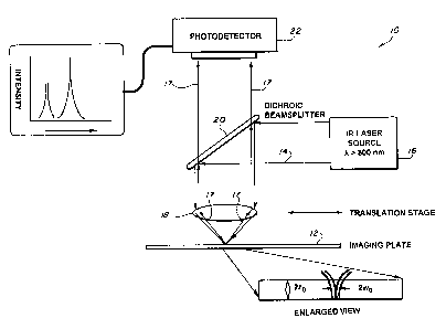
13 Fig. 1 shows a schematic of a typical laser scanned readout system 10
according to the
14 presently claimed invention.
Fig. 2 shows an alternative embodiment of a lamp illuminated readout system
according
16 to the present invention.
17 Fig. 3 shows another alternative embodiment of a laser scanned readout
system according
18 to the present invention.
19
Description of the Preferred Embodiments
21 The optically-stimulated luminescent imaging system described in this
invention utilizes
22 a novel, semiconductor- and/or metal ion-doped glass material that was
recently developed by
23 the present inventors and described in the United States Patent No.
5,811,822 and in United
24 States Patent No. 5,585,640 to Huston et al., the entirety of which is also
incorporated herein by
reference for all purposes. Basically, Huston et al. '822, describes a class
of optically
26 transparent, optically stimulated glasses and details three embodiments of
that class, along with
27 various methods of preparation.
28 Exposure of those composite glass materials to ionizing radiation, such as
deep
29 ultraviolet, x-ray or gamma radiation, results in the formation of trapped
electrons in the
composite glass material. The electrons remain trapped until the glass
material is exposed to
3
CA 02369026 2001-10-O1
WO 00/60375 PCT/US00/03316
1 light at a stimulating wavelength. Upon exposure to light at a stimulating
wavelength, the glass
2 emits a luminescent signal. Additionally, these glass materials scintillate
upon exposure to
3 ionizing radiation to provide a real-time image. To provide the best
possible resolution, the glass
4 material should be used in the form of a plate or sheet sufficiently thin to
satisfy the conditions
imposed for diffraction limited optics.
6 When used for real-time imaging, the present invention employs those
composite glass
7 materials in a manner analogous to the use of a phosphor screen in
conventional methods that
8 use a phosphor screen and a CCD camera. Basically, the glass materials of
the present invention
9 convert X-rays to photons by scintillation. A conventional lens-coupled
camera system, coupled
to a light sensor, for example a CCD sensor, images the photons. The light
sensor and its
11 associated conventional software convert the image to digital data, which
may then be stored,
12 printed or otherwise processed.
13 The ability of the Huston et al. optically transparent, optically
stimulated glasses to trap
14 charges upon exposure to u.v., x-rays or other ionizing radiation allows an
alternative to real-time
imaging methods. Trapped charges remain trapped until the phosphor is exposed
to an infrared
16 light source that is capable of releasing the traps and stimulating the
recombination of the charges
17 at a luminescent recombination center. The luminescence wavelength is in
the visible, and may
18 be recorded with a common, visible-light-sensitive photodetector. For
imaging applications, the
19 it stimulation light may come from a laser source that is focused to a
small spot and scanned over
the surface of the glass plate. Alternatively, a selected region of the glass
plate may be uniformly
21 illuminated with a lamp that is filtered to provide only light at
wavelengths in the infrared or near
22 infrared. This light stimulates luminescent recombination in the visible
that is detected and
23 imaged with a CCD camera.
24 In addition to the use of monolithic clear OSL glass sheets for recording
images, the OSL
glass may also be powdered and dispersed in a film such as a sol gel glass
film or a polymer film.
26 In the case of a sol gel film, a fine, e.g., one to two micron (400 mesh)
powder can be suspended
27 in an acidic solution consisting of an appropriate vehicle, such as
tetraethyl-orthosilicate,
28 methanol, and water, for the formation of thin glass film by a sol-gel
process.. The glass powder
29 may be used, for example, in a proportion of between about 1 % and about
10% by weight. A
thin film can be formed by dipping a substrate material into the sol-gel
solution and then
4
CA 02369026 2001-10-O1
WO 00/60375 PCT/US00/03316
1 withdrawing the substrate at a controlled rate. The substrate with the
applied film is then placed
2 in a furnace and heated to transform the organosilicate film into a purely
inorganic film. A film
3 prepared in this way will typically have a thickness of about 1 to about 2
microns and will appear
4 essentially transparent due to the refractive index match between the silica
powder and the sol-
gel-based film.
6 Instead of using a sol-gel solution, the powdered OSL glass may be dispersed
in a
7 polymer solution and then coated onto a substrate using the dip-coating
technique described
8 above. The polymer solution can contain any optically transparent polymer or
mixture of
9 polymers that can be dissolved in a solvent to an extent between about 1 %
and about 50% by
weight. Typically, a polymer solution with a dissolved solids content of about
5% to about 20%
11 by weight provides good optical quality film on a substrate material. A
mixture of polymers may
12 be used to reduce the refractive index difference between the polymer and
the glass powder
13 material thereby reducing scattering within the film. The polymer-glass
powder solution may
14 consist, for example, of a mixture of 1% to 50% by weight of
polymethylmethacrylate dissolved
in methyl ethyl ketone with the glass powder used in a proportion of between
1% and 50% by
16 weight. The thickness of the film can be controlled by varying the
viscosity of the polymer
17 solution. If desired, polymer-glass films can be prepared on or as flexible
substrates, for
18 example, by spin-coating a flexible substrate with the OSL glass powder in
either the sol-gel or
19 the polymer matrix, or by casting or extrusion of the sol-gel or polymer
matrix as a free-standing
film or sheet, to provide a flexible imaging medium. Such a flexible imaging
medium could be
21 useful for applications such as dental x-ray imaging.
22 The use of OSL powders still provides significant improvement in the
spatial resolution
23 of an image compared to the current art. As stated in the Description of
the Background Art, the
24 spatial resolution that can be achieved using current techniques is on the
order of tens of microns.
Crushing inorganic phosphors to smaller size diminishes their activity and
hence, their
26 sensitivity. OSL glass powders having grains sizes of 1 to 2 ~,m retain
their sensitivity. In
27 addition, the index of refraction of many OSL glass powders used in the
present invention is
28 ~ 1.4. Therefore, polymer or sol-gel films containing dispersed OSL glass
powder will be
29 optically transparent since many suitable polymer and sol-gel glass hosts
can be selected that
have an index of refraction of 1.4. The indices of refraction of inorganic
phosphors are typically
5
CA 02369026 2001-10-O1
WO 00/60375 PCT/US00/03316
1 larger (generally greater than about 3) and inorganic phosphor powders
dispersed in a polymer
2 or sol-gel glass film will not be index-matched. The resulting films using
inorganic phosphors
3 would scatter light to a significant degree, thereby limiting the achievable
spatial resolution of
4 the stored image.
Fig. 1 shows a schematic of a typical laser scanned readout system 10
according to the
6 presently claimed invention. For the highest resolution images, the
thickness of imaging plate
7 12 (for example, a sheet of the Huston et al. '822 glass) must satisfy the
conditions imposed for
8 diffraction limited optics. Specifically, the thickness of imaging plate 12
should be limited to
9 2*zo, where
zo = (nwo'-/Q), n is the index of refraction of the glass, p is the wavelength
of the light, and wo is
11 the radius of the laser spot size which is given by:
12 wo = 0.6351f/d, f is the focal length of lens 18 and d is the diameter of
the input, collimated light
13 beam at lens 18.
14 Referring again to Fig. 1, when laser beam 14 from source 16 is focused by
lens 18 onto
an exposed area of the imaging plate, the resulting stimulated luminescence 17
is collected by
16 lens 18, collimated, and directed back through a dichroic beamsplitting
mirror 20 and onto
17 photodetector 22. The intensity of the signal is proportional to the
exposure intensity. An image
18 in exposed imaging plate 12 is then obtained by translating image plate 12
in the plane of the
19 focus of lens 18 and measuring the luminescence 17 as a function of the
position of plate 12. The
glass material used for the imaging plate has a demonstrated dynamic range of
response of over
21 7 orders of magnitude. The combination of the dynamic range and the optical
transparency
22 provide for unprecedented optical image resolution.
23 Fig. 2 shows an alternative system 100 of the present invention using
microscope 102 and
24 CCD camera 104. Lamp 106 is a broadband incoherent light source such as a
tungsten lamp.
The output of lamp 106 is spectrally filtered by optical glass filter 108 that
transmits infrared and
26 near infrared radiation 109. The infrared radiation 109 uniformly
illuminates imaging plate 110,
27 stimulating visible luminescence 111 from those regions of imaging plate
110 that were
28 previously exposed to ionizing radiation. The colored glass filter 112
blocks the stimulation light
29 109 from interfering with the detection of the luminescence 111. The lens
or microscope
objective 102 images light 111 from all or part of imaging plate 110 onto CCD
camera 104. The
6
CA 02369026 2001-10-O1
WO 00/60375 PCT/US00/03316
1 magnification of the image is determined by the characteristics of the lens
or microscope 102.
2 The arrows show how the image may be inverted and magnified, without
distortion, by the
3 microscope objective.
4 An image stored on an OSL sheet may be read out using a device such as a
modified
flatbed scanner. As shown in Fig. 3, the light output from an OSL stimulating
light source, such
6 as a diode laser bar 102, can be projected to form an extended narrow line
104, and used in
7 conjunction with an extended linear CCD array 106 to record an image stored
in an OSL sheet
8 108. OSL sheet 108 can be translated with respect to light source 102 and
CCD array 106, or
9 light source 102 and CCD array 106 can be translated together while OSL
sheet 108 remains
stationary. A filter 110 can be placed in front of CCD array 108 to filter out
the stimulation light
11 and only allow passage of the OSL signal light.
12 The present invention has a number of useful applications. For example, the
present
13 invention is useful in quality control for photolithography.
Photolithographic processing
14 methods for integrated circuit chips are now capable of submicron feature
sizes. At the present
time, before a production run is undertaken, a test run is conducted to assure
that all of the
16 lithographic parameters are within specifications, including the beam
quality and the mask
17 integrity. This is a very time consuming process, requiring that the system
be opened up to
18 remove the test wafer, followed by etching and microscopic analysis of the
circuits. The present
19 invention provides a method for determining the beam quality and a high
resolution image of the
circuit without having to wait for a lengthy wafer processing procedure.
21 For nondestructive evaluation applications, an object may be placed on top
of a thin sheet
22 of the optically transparent phosphor glass and then exposed to an x-ray
source. Any
23 inhomogeneities present inside of the object, such as bubbles or cracks, or
material differences
24 such as metal lines will appear as contrast differences in the phosphor
image. The outstanding
dynamic range of the image storage material will allow for unprecedented
detection capabilities.
26 Medical imaging applications include mammography and osteoporosis
screening. The
27 enhanced resolution and dynamic range will provide improved diagnostics for
detecting and
28 distinguishing between fibrous cysts and cancerous tumors in breast tissue
and allow very precise
29 measures of variations in bone density.
The present invention also has applications in stereotactic imaging: High
precision
7
CA 02369026 2001-10-O1
WO 00/60375 PCT/US00/03316
1 radiotherapy procedures require extensive modeling using phantoms for
treatment planning. Part
2 of the planning process involves obtaining images of the radiation beam
profile near the focal
3 region. The glass imaging plates of the present invention provide
significant advantages over
4 currently used films. The glasses offer orders of magnitude improvements in
dynamic range and
are reusable.
6 Obviously, many modifications and variations of the present invention are
possible in
7 light of the above teachings. It is therefore to be understood that, within
the scope of the
8 appended claims, the invention may be practiced otherwise than as
specifically described.
8