Note : Les descriptions sont présentées dans la langue officielle dans laquelle elles ont été soumises.
W~ 01/61079 CA 02369687 2001-10-11 pC'1'/[JSOl/0123$
Title: Process for electroplating a work piece coated with an electrically
conducting polymer
The invention refers to a process for electroplating a work piece, which is
coated with an electrically conducting or modified polymer. In addition, the
invention shows apparatus for carrying out this process.
For the targeted change of the surface, or of the surface structure, of two
and three dimensional work pieces, electroplating, even in the case of non-
metallic surfaces, is a process which corresponds to the state of the art and
which
often is used in practice. Thus, for example in the manufacture of a circuit
board,
metallizing and complete contact formation of the base material is achieved by
electroplating. Generally, the base material consists of an insulator where a
large
portion of the surface, which is to be electroplated, is coated with an
electrically
conducting or modified, polymer.
However, the deposition of a metallic coating on the large area of an
insulator coated with an electrically conducting polymer by electroplating is
usually only possible with considerable effort. Due to the fact that even a
2o modified polymer has a high specific electrical resistance compared to a
metallic
material, the current density on the surface of the work piece to be
electroplated is
distributed in an uneven manner so that an evenly strong electrical field does
not
develop. In order to still achieve a continuous metal coat either the current
density must be increased or the electroplating time must be extended.
In order to avoid the disadvantages connected with extending the
electroplating time, it is known from the current state of the art to increase
the
current density. However, an excessive current density in the contact area
leads to
the destruction of the electrically conducting polymer coating. An
electroplated
metal deposition can then no longer take place, due to the diminished
electrical
3o conductivity. In order to avoid such a destruction of the polymer coating,
an
appropriately low current density must be selected which results in an
extension of
the electroplating time and the attendant disadvantages.
It is therefore necessary for electroplating a work piece coated with an
electrically conducting polymer to determine and to balance the current
density
WO 01/61079 CA 02369687 2001-10-11 PCT/USO1/01235
2
and the electroplating time appropriate to the work piece. In order to obtain
a
coating without voids it is therefore necessary to consider the balance
between
excessive current density on the one hand and an excessive electroplating time
on
the other, whereby the work piece-related parameters are to be determined
again.
Thus large-scale applications of the processes known from the current state of
the
art are not satisfactory since either very time-consuming adjustments must be
made or a high failure rate results if these adjustments are not made.
In order to avoid the disadvantages mentioned it is therefore the intent of
the invention to describe a method for electroplating of a work piece which is
1 o coated with an electrically conducting polymer which is independent of the
work
piece to be electroplated and which permits a shortening of the electroplating
time
while, at the same time, reducing the current density.
According to the invention this problem is solved by connecting the work
piece in the first step of the process to a current source by multiple
adjacent
contact elements and coating with a continuous, thin metal layer except at the
contact locations covered by the contact elements. The contact elements are
removed in a second process step, and an unbroken, continuous coat is formed.
It is further proposed by the invention to cover the work piece to be
electroplated with a multitude of adjacent contact elements so that a
multitude of
2o current-carrying connections between the surface to be electroplated and
the
current source are formed. This has the advantage that an electrical field is
generated even with only a low current density, which is sufficient for
electroplating the surface. The electrically conducting polymer coating is
connected to the current source so that an almost uniform electrical field is
generated covering the entire surface of the work piece to be electroplated.
In the first step of the process described by the invention, after connecting
the contact elements to the current source, a thin metal layer is formed on
the
electrically conducting polymer coating of the work piece to be electroplated.
This metal layer is unbroken except for the contact points covered by the
contact
3o elements. The contact elements are laid out on the surface to be
electroplated in
such a manner that the metal layer deposited in the first step of the process
extends over the entire surface and forms a continuous metal coat. Due to the
multitude of the contact elements used, the build-up of the metal coat
requires
WO 01/61079 CA 02369687 2001-10-11 pCT/USOl/01235
3
only a relatively short electroplating time. It is of advantage that despite
the
reduction of the current density the electroplating time does not increase. To
the
contrary, the process described by the invention presents the possibility to
also
reduce the electroplating time despite the reduced current density. The
disadvantages of the processes known from the current state of the art
represented
by a destruction of the polymer coating, due to an excess of current density
or due
to an excess of electroplating time can be entirely avoided by the use of the
process described by the invention.
After the deposition of the continuous metallic coat, except the points
1 o covered by the contact elements, these are removed in the second process
step,
and the surface area to be electroplated is charged with current through the
metal
coat formed in the first process step. A metal deposit now also forms at the
contact points covered by the contact elements during the first process step,
so that
a unbroken metal coat forms over the entire surface of the work piece to be
1 ~ electroplated. During this second electroplating step also only relatively
low
current densities as well as short electroplating times are required since the
metal
coat formed in the first process step covers the surface area, and thus a
generally
homogeneous electrical field is built also with low current density. In
addition, in
contrast to a polymer coat, the metallic coat represents a good electrical
conductor
2o with a low specific resistance.
The second process step intended for the formation of an unbrokenly
continuous metal coat can be carried out in accordance with the invention in
such
a manner that the contact points not yet covered after the completion of the
first
step are provided with a metal coating, so that in this manner the contact
points
25 still remaining open are "closed", and an unbroken metal coat is formed in
the
second process step. The second process step can also be carried out in such a
manner that the metal coat formed in the first process step keeps growing so
that
an unbroken metal coat is formed which also covers the contact points. The
second process step can also be carried out using a different electrolyte
3o composition, for example. When carrying out this process, it is important
that the
connection of the work piece to be coated is by multiple adjoining contact
elements so that a generally homogeneous electrical field is built over the
entire
surface. The contact points covered up by the contact elements of the surface
to
WO 01/61079 CA 02369687 2001-10-11 pCT~S01/01235
4
be coated can then be closed by the formation of an unbroken metal coating
in a second process step.
With the process described in the invention, it is possible for the first time
to provide a two or three dimensional work piece with an electrically
conducting
polymer coat with a metal coating by electroplating, whereby in spite of
reduced
current density only a relatively short electroplating time is required. The
disadvantages of the known processes from the current state of the art which
result
in the destruction of the polymer coat due to excessive current density and
due to
excessive electroplating time can therefore be avoided. An electroplating
process
1 o conducted as described in the invention permits the mass production of
electroplated work pieces since with regard to the current density to be set
and the
electroplating time to be selected, the greatest independence from the work
piece
to be electroplated is achieved, and also a costly readjustment of these
process
parameters prior to the beginning of each new electroplating process is not
required.
In accordance with one characteristic of the invention, the individual
contact elements on the surface to be electroplated are placed lattice-like
next to
each other. In this manner it is achieved that both in the first process step
in
which the surface to be coated is connected to the current source over the
contact
2o elements and also in the second process step when the current supply takes
place
over the metal coating formed in the first process step an extensive, evenly
formed
electrical field extends over the entire surface area to be electroplated. In
addition, it is achieved that the metal coat to be formed in the first process
step by
itself constitutes a continuous electrical conductor. It is therefore
suggested that it
is especially advantageous if neighboring contact elements are laid out
equidistant.
In accordance with another characteristic of the invention, a contact
element carrier is used for the contact element layout, which comprises
several
contact elements. On the one hand, a quick placement of the contact elements
on
3o the surface to be electroplated is achieved in this manner, on the other
hand, the
use of a contact element carrier permits extensive automation of the process
described in the invention. The contact element carrier preferably is designed
in
such a manner that it comprises multiple adjoining contact elements which can
be
WO 01/61079 CA 02369687 2001-10-11 pCT/LTSOl/01235
moved from their relative position for adjustment purposes, whereby
adjustment of the contact elements relative to each other as well as to the
contact
element carrier itself is possible. Depending on the work piece to be
electroplated, adjustment of the contact elements is possible so that it can
be
5 ensured that all contact elements to be placed on the surface of the work
piece to
be electroplated actually establish an electrical connection between the work
piece
to be electroplated and the current source. In this manner, it can be avoided
that
voids appear in the metal coating to be formed.
In accordance with a first alternative, a frame with mounted contact
1 o elements is used as a contact element carrier. Such a frame-like contact
element
carrier is especially suitable for electroplating of 2-dimensional work pieces
such
as, for example, circuit boards. As suggested by the invention, such a frame
is
rectangular in shape while other geometric shapes are conceivable, depending
on
the type of application. Multiple contact elements are mounted on the frame
which are placed either on all or on individual components forming the frame.
For the connection of the surface to be electroplated to the current source,
this is
contacted by the elements of the frame-shaped contact element carrier. In this
connection, in accordance with a further characteristic of the invention, for
large
area coverage, several frames can be placed next to each other or on either
side of
2o the work piece to be electroplated. It is especially attractive in the case
of circuit
boards, to metal-coat the basic raw circuit board on both sides in the course
of one
process step.
In accordance with a further characteristic of the invention, a fixture with
multiple contact elements is used as contract element carrier. A fixture of
this
type especially serves the connection of a 3-dimensional work piece. This is
inserted into a fixture designed for this purpose and connected to the current
source over the contact elements attached to the fixture. In this manner it is
made
possible to unbrokenly electroplate even a geometrically complex work piece in
one process step. It is self evident, of course, that in addition to the
design of the
3o contact element carrier as a frame or as a fixture other forms are
conceivable. The
deciding factor is that the surface of the work piece to be electroplated can
be
covered area-wide by the contact element carrier with multiple contact
elements.
WO 01/61079 CA 02369687 2001-10-11 pCT/USOl/01235
6
In accordance with a further characteristic of the invention,
the contact elements are designed to be movable in their relative position on
the
one hand to each other, as well as to the contact element carrier on the other
hand;
and that they can be adjusted for contact with the work piece to be
electroplated
for connection to the current source, depending on the work piece geometry.
Thus, it can be ensured that by means of the process described by the
invention
not only regularly shaped work piece surfaces but also irregularly shaped,
complex geometric forms can be covered over their entire area by contact
elements, and the work piece to be electroplated can be connected to the
current
l0 source.
In accordance with a further characteristic of the invention, a metallic grate
is used as the contact element carrier. The metallic grate is especially
suited to
horizontal applications in continuous processing facilities. This metallic
grate
constitutes a complete electrical conductor so that its placement on the
surface to
be electroplated leads to the build-up of a general, homogeneous electrical
field.
Thus, within a relatively short time, and using only a low current density, a
metallic coat can be formed which basically constitutes a negative of the
grid. In
other words, the areas of the surface to be electroplated not covered by the
grid are
covered with a metal layer. In a second step of the process, the grid can then
be
2o removed and a closed metal coating formed on the surface. In accordance
with an
advantageous characteristic, the surface to be electroplated is contacted by
the
grid, and the work piece together with the grid is fed through the
electrolyte.
Thus, the grid simultaneously also serves as a conveyor. In this manner, given
short cycle rates and ease to automate, and above all reproducible, surfaces
of
2s work pieces can be electroplated in accordance with the process described
by the
invention. In order to ensure that the metal grate placed on the work piece to
be
electroplated can be removed without destroying the underlying polymer coat
after the deposition of the first metal coating, it is another characteristic
of the
invention that counter anodes are supplied by which the metal deposited from
the
3o metallic grid is loosened from the work piece.
In accordance with a further characteristic of the invention, the thickness
of the metal coat produced by the process, which is the subject of the
invention,
can be specified. This can be adjusted, on the one hand by the dwell time of
the
WO 01/61079 CA 02369687 2001-10-11 pCT/USOl/01235
7
work piece in the electrolyte, and by the connected current density on the
other.
In any case, it is possible to build a metal coat of the required thickness
adapted to
the later demands on the finished work piece.
Additional details, characteristics and advantages of the invention are
discussed in the following descriptions of the enclosed drawings:
Fig. 1 is a schematic of the first step of the process described by the
invention for
the manufacture of a circuit board in the vertical process.
Fig. 2 is a schematic of the second step of the process described by the
invention
for the manufacture of a circuit board in the vertical process.
1o Fig. 3 is a schematic of a grate serving as a contact element carrier.
Fig. 4 is a schematic of the first step of the process described by the
invention for
the manufacture of a circuit board in the horizontal process.
Fig. 5 is a schematic section of a contact element in accordance with a first
application design.
Fig. 6 is a schematic section of a contact element in accordance with a second
application design.
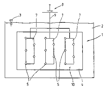
Fig. 1 shows the manufacture of a circuit board 1 in accordance with the
process described in the invention. Here, the first step of the process is
shown. In
electrolyte 2, generally perpendicular to the electrolyte surface 3, a base
body 4
2o made of an insulator and coated with an electrically conducting or modified
polymer layer is inserted. Due to the fact that the base body 4 is moved
generally
perpendicular to the electrolyte surface 3, this process may also be referred
to as a
vertical process.
The base body 4 is connected to the current source 8 over multiple contact
elements 5. This is achieved by a branching electric wire 9. As can be seen in
Fig. 1 schematically, all contact elements 5 are placed onto the base body 4
which
is to be electroplated and make electrical contact with the current source 8
by
means of the contact element carriers 7. For example, the figure shows three
frame-shaped contact element carriers 7 with five contact elements ~ attached
to
3o each. The contact elements 5 are fixed to each of the contact element
carriers in
such a manner that they are movable both relative to each other and relative
to the
contact element carrier 7, so that individual adjustment of the contact
elements 5
can be made with reference to the size or geometric shape of the base body 4
W~ 01/61079 CA 02369687 2001-10-11 pCT~S01/01235
8
which is to be electroplated. After applying the current, based on the
multiple contact elements 5 used, a nearly homogeneous electrical field is
built up
which extends over the entire surface of the base body 4 to be electroplated.
As a
result of the build-up of the even electric field extending over a wide area,
an
unbroken, thin metal coat 10 forms within a short time at a relatively low
current
density except at the contact points 6, covered by the contact elements 5. By
the
use of multiple contact elements 5 electroplating can occur within a short
electroplating time, despite a low current density.
Fig. 2 shows the second process step as described in the invention. After
l0 the build-up of the metal coat 10 with the exception of the contact points
6
covered by the contact elements 5, the contact elements are removed and an
unbroken metal coat is formed. For this, the metal coat produced in the first
process step is connected to the current source 8 by means of the electric
wire 9.
In this manner, an also nearly homogeneous electrical field is built up which
leads
to the still void spots in the metal coat 10 being closed by metal deposition,
and an
unbroken metal coat is created. After the build-up of the specified layer
thickness
of the metal coat, the base body 4 is again removed from the electrolyte 2.
Fig. 3 shows an alternative version of a metallic grate 11 which serves as
an area contact element and which is provided with insulation except for the
2o contact points. In the first process step the work piece to be
electroplated is laid
onto the grate 11 with the surface to be electroplated toward the grate and
fed
through the electrolyte 2 in the horizontal process. This is shown
schematically in
Fig. 4. This can be viewed as grate 11 forming an endless band which, at the
same time, serves as the conveyor. By means of reversing rolls 12 the grate 11
is
moved by a drive unit 13 in the transport direction 14. The grate 11 is
connected
to a current source 8 by sliding contacts 15, for example. For the
manufacture, for
example of circuit boards, the base bodies 4 are laid on the grate 11 at the
loading
station 16. The loading station 16 is located outside the electrolyte tank 17.
The
base bodies 4 laying on the grate 11 are transported in direction 14 and
inserted
3o into electrolyte tank 17 and immersed in the electrolyte 2. Due to the fact
that the
grate 11 generally runs parallel to the electrolyte surface 3 this process is
also
referred to as the horizontal process, in contrast to the previously mentioned
vertical process. As a result of the wide area coverage of the surface of the
base
W~ O1/f)1079 CA 02369687 2001-10-11 pCT/US01/01235
9
body 4 to be electroplated, only a relatively weak current density and a
short electroplating time are required for the formation of a first metallic
coat.
After the build-up of this metal coat, the base bodies 4 are removed from the
electrolyte tank 17 in the direction 14 and transported to the unloading
station 18.
There, the base bodies 4 are removed from the grate 11. In order to avoid
permanent electroplating of the contact points, the metal deposited there can
be
dissolved by means of the counter anode 19. Subsequent to the completion of
the
first process step and the build-up of metal coats in accordance with Fig. 4,
there
follows in a manner similar to the vertical process already described above,
the
1 o build-up of the unbroken metal covering.
Fig. 5 and 6 each show two alternatives of a contact element 5 located on a
contact element carrier 7. The contact elements shown in Fig. 5 and 6 differ
due
to their relative movability in the lifting direction 20. This is achieved by
a
suitable spring element. Individually, the contact elements are designed as
follows: The current-carrying contact pin 21 is movable radially relative to
the
base body 4 (lifting direction 20). The contact pin 21 is surrounded by
insulation
22 and attached to the contact element carrier 7 by a threaded connector 23.
This
design has the advantage of fitting the contact element 5 also to a non-level
surface of the base body 4. By this method it is ensured that multiple contact
2o elements 5 contact the base body 4, and thus an electrical connection is
established between the base body 4 and the current source 6.
WO 01/61079 CA 02369687 2001-10-11 PCT/USOl/01235
Reference kev list
1 Circuit board
2 Electrolyte
5 3 Electrolyte surface
4 Base body
5 Contact element
6 Contact point
7 Contact element
carrier
10 8 Current source
9 Electric wire
10 Metal coating
11 Grate
12 Reversing rolls
13 Drive unit
14 Transport device
15 Sliding contact
16 Loading station
17 Electrolyte tank
18 removal station
19 Counter anode
20 Stroke direction
21 Contact pin
22 Insulation
23 Connecting unit