Note : Les descriptions sont présentées dans la langue officielle dans laquelle elles ont été soumises.
CA 02370596 2001-11-02
WO 00/67107 PCT/US00/12433
SYSTEMS AND METHODS FOR A DISK CONTROLLER MEMORY ARCHITECTURE
Field of the Invention
The present invention relates generally to disk controllers and more
particularly to disk controllers having a
multiported memory architecture.
Background of the Invention
Conventional computer systems typically include several functional units.
These functional units may include a
central processing unit (CPU), main memory, input/output devices, and magnetic
disk drives. In conventional systems, the
main memory is tightly coupled to the CPU via a system bus or a local memory
bus. The main memory is used to provide
the CPU quick access to data or program information that is stored in main
memory at execution time. Typically, the main
memory is composed of random access memory (RAM) circuits. A computer system
including the combination of the CPU
and the main memory is often referred to as a host system.
The main memory is typically smaller than the magnetic disk drive. The main
memory is usually volatile, while
the magnetic disk drive is non-volatile. Therefore, programming data
information is often stored on the magnetic disk drive
and is read into the main memory as needed. In contrast to the main memory,
which is closely coupled to the CPU, the
magnetic disk drive is usually more remotely coupled to the CPU. Because the
magnetic disk drive is more remotely
coupled to the CPU, access to the magnetic disk drive is typically slower and
more complicated than access to the main
memory. A disk controller typically couples the host system to the magnetic
disk drive and handles the complex details of
interfacing the magnetic disk drive to the host system. Communications between
the host system and the disk controller is
usually provided using one of a variety of standard IIO bus interfaces.
The magnetic hard disk drive assembly usually consists of one or more magnetic
disks. Each disk typically has a
number of concentric rings or tracks on which data is stored. The tracks
themselves are further divided into sectors which
are the smallest accessible data unit. A sector is accessed by positioning a
magnetic head above the appropriate track.
The first sector of a track is typically identified by an index pulse. The
start of each other track sector is identified with a
sector pulse. The drive waits until the desired sector rotates beneath the
head and then proceeds to read or write the
data. The date is accessed serially, one bit at a time. Usually, each disk in
the disk drive has its own read/write head.
The disk drive is connected to the disk controller. The disk controller
performs numerous functions, such as, for
example, converting digital data to analog head signals, converting analog
head signals to digital data, disk formatting, error
checking, logical-to=physical address mapping, and data buffering. For
example, the disk drive typically formats the data
from the drive. The data from the drive is serially arranged and the disk
controller converts the serial data into a parallel
arrangement.
The data buffering function is used in transferring data between the host and
the mass storage memory. Data
buffering is needed because the speed at which the disk drive can supply or
accept data from the host is different then the
speed at which the host can correspondingly read or supply the data.
Therefore, the disk controller conventionally contains
a buffer memory that temporarily stores data being read or written to the hard
drive to synchronize the data with the speed
of the 110 bus to which it is connected. Thus, the buffer decouples the rate
at which data is exchanged between the drive
SUBSTITUTE SHEET (RULE 26)
CA 02370596 2001-11-02
WO 00/67107 PCT/US00/12433
and host and the rate at which data is written and read from the drive. The
buffering function is particularly necessary
because each sector is read or written as a whole.
In addition to providing access to both the IIO bus and the disk drive, the
buffer memory often is accessed by a
local processor on the disk controller. Thus, the disk controller buffer
memory may be accessed by many functional
portions of the disk controller and by the host. In conventional systems, the
competition for access to the buffer memory
is often a bottleneck which greatly restricts the data transfer rates between
the buffer memory and the functional units,
as well as to the disk drive and the host.
Another performance bottleneck found in conventional disk controllers is the
local processor. The local processor
typically manages an IIO bus interface circuit, the buffer memory, the disk
formatter, as well as management of the disk
controller as a whole. Furthermore, conventional systems require the local
processor to manage data transfers through the
buffer memory at a low level. Typical general-purpose processors are
inadequate to handle such application specific
functions in an efficient manner.
In addition, conventional disk controllers do not fully utilize their
processors. For example, if, while
transferring data from the disk to the 110 bus using one or more the disk
controller processors, the transfer outpaces
the disk's ability to supply data, the processors are wastefully paused until
the disk catches up.
Summary of the Invention
The present invention is generally related to efficient and flexible methods
and systems of buffering and
accessing data being written to or read from mass storage devices.
In one embodiment, a disk controller includes a data buffer used to buffer
data transferred between a mass
storage device and an IIO bus. In another embodiment, the data buffer includes
a multi-port memory. The muiti-port
memory is coupled to a plurality of channels, such as, by way of example, a
disk channel and an IIO channel, as well as one
or more processors.
In one embodiment, the multi-port memory may be used as both a random access
memory and a first-in-first-out
(FIFO) memory. Thus, when used as a first-in-first out memory, the multi-port
memory may be used to buffer data between
the disk channel and 110 channel. The multi-port memory may be used for
context switching, wherein register data from
one or more processors is swapped in or out of the memory. The efficient
register swapping provided by one embodiment
of the present invention advantageously allows the processor to quickly switch
between tasks. This is very useful if a first
task is in a wait state, because rather than wasting processor time pausing
while waiting for the wait state to end, the
processor can quickly switch to another task, and then, after the wait state
has ended for the first task, switch back to
the first task.
In addition, in one embodiment, the random access feature allows selected data
stored in the multi-port memory
to be swiftly retrieved. For example, if the memory is used to store a Fibre
Channel frame and associated CRC data, the
CRC data can be immediately retrieved without having to read out the entire
frame.
In one embodiment, the multi-port memory is a DMA (direct memory access)
memory. In an exemplary
embodiment, the multi-port memory's ports include a random access port, a FIFO
access port, a register access port, andlor
-2-
SUBSTITUTE SHEET (RULE 26)
CA 02370596 2008-12-16
a buffer controller DMA port. The random access port is connected to a
microprocessor interface bus
which in turn is connected to one or more processors, such as a microprocessor
and a microcontroller,
as well as the FIFO access port. The register access port is may also be
connected to one or
processors, such as a microcontroller. The buffer controller DMA port is
connected to a CRC (cyclic
redundancy code) checker and to a buffer memory.
In one embodiment, the multi-port memory contains 64 bytes and can hold an
entire Fibre
Channel protocol command. Furthermore, a state machine associated with the
multi-port memory can
perform several commands. In another embodiment, one or more of the commands
are configured to
efficient manage I/0 packets or frames. In yet another embodiment, the state
machine commands
include one or more of the following: a fetch current FCP (Fibre Channel
Protocol) command, an update
current FCP pointer command, a load FIFO command, an unload FIFO command, a
load FIFO with
CRC, an unload FIFO with CRC, a write to buffer memory command, and a read
from buffer memory
command. In one embodiment, a command is provided that causes the transfer of
an entire Fibre
Channel command into the FIFO without further intervention from the
microprocessor or the
microcontroller. One embodiment provides direct frame access to Fibre Channel
frames. In another
embodiment, the commands may be halted and/or paused.
In accordance with an aspect of the present invention, there is provided a
disk drive controller
circuit including a flexible, multiported memory circuit that allows data to
be efficient accessed or stored,
comprising:
a disk drive interface;
an I/0 interface;
a buffer memory coupled to transfer data to and from said disk drive interface
and to and from
said I/0 interface;
a first processor used to at least control said disk drive interface;
a second processor used to at least perform low level tasks; and
a memory circuit including:
a DMA port coupled to said buffer memory;
a register access port coupled to said first processor and said second
processor;
a random access port coupled to said first processor and said second
processor; and
a read pointer and a write pointer accessible by at least one of said first
and second
processors.
In accordance with another aspect of the present invention, there is provided
a disk drive
controller, comprising:
a disk drive interface;
a buffer memory coupled to at least receive data from said disk drive
interface;
a first processor; and
3
CA 02370596 2008-12-16
a memory circuit loadable using direct memory access coupled to said buffer
memory and said
first processor, said memory circuit configured to operate as a first-in-first-
out memory when transferring
data between said buffer memory and said memory circuit during a first
transfer via a first port, and said
memory circuit configured to operate as a random access memory when being
accessed by said first
processor during a second transfer via a second port.
In accordance with another aspect of the present invention, there is provided
a mass storage
device controller for interfacing a computer to a mass storage device, said
mass storage device
controller comprising:
a mass storage buffer memory interface;
a processor; and
a first memory circuit loadable using a direct memory access transfer
configured to be coupled
to receive data from said mass storage buffer memory interface in a first-in-
first-out manner using a first
port, said memory circuit accessible by said processor as a random access
memory using a second
port.
In accordance with another aspect of the present invention, there is provided
a mass storage
device controller for interfacing a mass storage device to a computer via an
I/0 bus, said mass storage
device controller comprising:
a buffer memory configured to receive data from said mass storage device and
data from said
I/0 bus;
a processor; and
a memory circuit coupled to said buffer memory and said processor, said memory
circuit
configured to operate as a first-in-first-out memory during at least a first
transfer of data between said
memory circuit and said buffer memory, and said memory circuit configured to
operate as a random
access memory during at least a first transfer of data between said memory
circuit and said processor.
In accordance with another aspect of the present invention, there is provided
a system for
controlling a mass storage device, comprising:
a host computer;
a bus coupled to said host computer;
a mass storage device; and
a controller coupled to said bus and said mass storage device, said controller
including:
a first memory circuit configured to receive data from said mass storage
device and
data from said I/0 bus;
a processor; and
a second memory circuit coupled to said first memory circuit and said
processor, said
second memory circuit configured to operate as a first-in-first-out memory
during at least a first
transfer of data between said second memory circuit and said first memory
circuit, and said
3a
CA 02370596 2008-12-16
second memory circuit configured to operate as a random access memory during
at least a
first transfer of data between said second memory circuit and said processor.
In accordance with another aspect of the present invention, there is provided
a mass storage
device controller for interfacing a mass storage device to a computer via an
I/0 bus, said mass storage
device controller comprising:
a means for receiving data from said mass storage device and data from said
I/0 bus;
a means for managing said mass storage device controller; and
a means for storing data coupled to said means for receiving data and said
means for
managing, said means for storing data configured to operate as a first-in-
first-out memory during at least
a first transfer of data between said means for storing data and said means
for receiving data, and said
means for storing data configured to operate as a random access memory during
at least a first transfer
of data between said means for storing data and said means for managing data.
In accordance with another aspect of the present invention, there is provided
a method of
transferring data between memories in a mass storage device controller, said
method comprising the
acts of:
transferring a buffer length field associated with a data packet from a first
memory to a first
location of a second memory operable as a first-in-first-out (FIFO) memory,
wherein at least a portion of
the buffer length field includes information related to the amount of data
being transferred via the data
packet;
transferring at least a portion of said data packet from said first memory to
at least a second
location of said second memory; and
reading said buffer length field from said memory operable as a FIFO memory,
and then
reading said at least portion of said data packet from said second memory.
In accordance with another aspect of the present invention, there is provided
a method of
accessing and storing data in a disk drive controller, comprising:
receiving data in a buffer memory;
transferring data from the buffer memory to a multiported memory located on
the disk controller
using a first port of the multiported memory, wherein the first port is a
first-in-first-out port;
transferring data between the multiported memory and a first disk controller
processor using a
second port of the multiported memory, wherein the first disk controller is
configured to perform high-
level tasks; and
transferring data between the multiported memory and a third disk controller
processor using a
third memory port of the multiported memory, wherein the second disk
controller is configured to
perform low-level tasks.
Brief Description of the Drawings
Figure 1 is an illustration of one environment using one embodiment of the
present invention;
Figure 2 is an illustration of the ports of one embodiment of a buffer
controller;
3b
CA 02370596 2008-12-16
Figure 3 is a more detailed illustration of the buffer controller of Figure 2;
Figure 4 illustrates one embodiment of a memory unit;
Figures 5A-D illustrate one embodiment of a state machine used with the buffer
controller;
Figure 6 is an illustration of one embodiment of data translation;
Figure 7 is an illustration of a Fibre Channel control block;
Figure 8 is an illustration of a first exemplary data transfer;
Figure 9 is an illustration of a second exemplary data transfer;
Figure 10 is an illustration of a third exemplary data transfer;
Figure 11 is an illustration of a fourth exemplary data transfer;
Figure 12 is an illustration of a fifth exemplary data transfer;
Figure 13 is an illustration of a sixth exemplary data transfer;
Figure 14 is an illustration of a seventh exemplary data transfer; and
Figure 15 is an illustration of an eighth exemplary data transfer.
Detailed Description of a Preferred Embodiment
The present invention is generally related to efficient and flexible methods
and system for
buffering data being written to or read from a mass storage device.
As illustrated in Figure 1, in one embodiment of an electronic system 100, a
disk controller 102
is used to interface a host system 104 to a mass storage device 106, such as a
magnetic disk drive or
an optical disk drive, via a disk port 136. The illustrated disk controller
102 includes a microprocessor
108, an embedded controller 110, buffer memory
3c
CA 02370596 2001-11-02
WO 00/67107 PCT/US00/12433
112, and an external DMA (direct memory access) device 114. The disk
controller is coupled to the host system 104 via
an IIO bus 116, such as a Fibre Channel bus having dual loops. The embedded
controller 110 includes a microprocessor
interface 118 which is coupled to the microprocessor 108. A microprocessor bus
130 couples the microprocessor
interf ace logic 118 to the external DMA interface 134, a microcontroller 120,
a buffer controller 122, and a Fibre Channel
interface 124 located within the embedded controller 110. The external DMA
interface 134 in turn is coupled to the
external DMA device 134 and to the buffer controller 122. The buffer
controller 122 is also coupled to the buffer memory
112 and to the Fibre Channel interface 124. The Fibre Channel interface 124 is
coupled to Fibre Channel loops 116 via
Fibre Channel transmit and receive circuitry within the interface 124. The
Fibre Channel loops 116 are also connected to
one or more hosts 104. The Fibre Channel interface 124 can be used to
communicate both Fibre Channel protocol and
SCSI protocol.
A data flow controller 126 is coupled to the external DMA interface 134, the
buffer controller 122, and the
Fibre Channel interface 124. An ECC engine module 132 is connected to the disk
formatter 128, the buffer controller 122,
and the Fibre Channel interface 124, via the data bus 126.
The Fibre Channel interface 124 implements the Fibre Channel protocol. In one
embodiment, the Fibre Channel
interface 124 implements the FC-AL (Fibre Channel Arbitrated Loop) protocol
including the FC-1 and FC-2 layers of the
Fibre Channel signaling interface. The Fibre Channel interface 124 includes an
encoder and decoder and a frame buffer for
clock skew management and a Fibre Channel protocol handler machine. The Fibre
Channel interface 124 validates and
routes data trains received from the Fibre Channel loops to appropriate areas
in the frame buffer. The transmit path of the
Fibre Channel interface 122 transmits frames from the frame buffer to the
Fibre Channel. The Fibre Channel interface
automatically handles frame delimiters and frame control.
In one embodiment, the disk formatter 128 provides an interface to the disk
106. The disk formatter 128
receives control information and parameters from the local processor 108. The
disk formatter 108 then carries out the
requested action. The microprocessor may also handle other tasks, such as
signal processing for servo control of the disk
head, and SCSI protocol management, which may be used to communicate data over
the Fibre Channel. The
microcontroller 120 may be used to perform other tasks, including low level
tasks such as Fibre Channel transfer
management tasks, thereby offloading the processor 108. Thus, in one
embodiment, the controller workload is
advantageously divided among multiple processors, allowing for more efficient
task execution.
In one embodiment, the microcontroller 120 is an 8 bit machine which can
support either 8 bit or 16 bit DMA
transfers. In addition, the microcontroller 120 has registers and an internal
ALU, including an accumulator used for
mathematical operations.
In one embodiment, the buffer controller 122 is a multiple channel DMA
controller integrated with a synchronous
DRAM (SDRAM) controller. In another embodiment, the buffer controller 122
supports buffer sizes of up to four
megabytes. However, in still another embodiment, sizes greater or less than
four megabytes are supported as well. The
buffer controller 122 provides for high-speed buffer memory 112 initialization
and verification and reduces power upon
initialization. The buffer controller 122 also provides controls to the buffer
memory 112, which, in one embodiment, is
-4-
SUBSTITUTE SHEET (RULE 26)
CA 02370596 2001-11-02
WO 00/67107 PCTIUSOO/12433
implemented using synchronous DRAM (SDRAM). However, other memory
architectures, such as asynchronous RAM or
static RAM, can be used as well.
Buffer management is provided by a four-channel, high speed, bursting DMA
controller. The buffer controller
122 provides an interface between a variety of modules and interfaces,
including, by way of example, the buffer or holding
memory 112, the disk channel, an ECC channel, the Fibre Channel, the
microprocessor 108 and the microcontroller 120.
The buffer controller 122 regulates and buffers data movement into and out of
the SDRAM buffer memory 112. Each
DMA channel supports DMA bursting of multiple blocks of data, allowing high
bandwidth transfers. Each DMA channel
has associated control, configuration, and buffer memory address registers. In
one embodiment, the buffer memory 112 is
shared by other units which are provided with access-turns or access tenures.
Within the tenure, a given data source
bursts data until the transfer is complete or an assigned tenure time has
expired. However, many of the DMA channels are
connected to modules running on a different clock or at a different speed than
that of the buffer controller 122. Hence, as
discussed below, a memory unit configurable as a FIFO (first-in-first-out)
memory is used to synchronize and buffer channel
data.
The buffer controller 122 also provides microprocessor address decoding,
priority arbitration for the buffer
resource, block CRC (BCRC) checking, and automatic DRAM refresh control. In
one embodiment, a CRC calculatorlchecker
includes an accumulator with feedback.
The data flow controller 126 reduces data transfer time by, in one embodiment,
automatically monitoring and
controlling the flow of data between the disk 106 and the Fibre Channel ports.
Automatic control of data flow between
these channels reduces the number of interrupts that occur in a typical disk-
to-Fibre Channel data transfer. In addition, the
data flow controller 126 automatically helps prevent buffer overflow and
underflow conditions while temporarily
suspending or pausing the disk formatter or the Fibre Channel DMA channel
before the buffer becomes full or empty.
Exemplary data flow operations between the host 104 and the disk 106 will now
be described. A typical write
operation proceeds as follows. The host 104 sends a write command over the
Fibre Channel bus 116 to the disk controller
102. The command passes through the Fibre Channel interface 124 and is then
loaded via the bus controller 124 into the
buffer memory 112. The host path to the disk controller is termed Channel 1.
Once the write command is written into the
buffer memory 112, the microprocessor 108 reads the command out of the buffer
memory 112 and appropriately sets up
the disk controller registers in preparation for the commanded write
operation. The disk controller registers include
registers associated with the buffer controller 122, the disk formatter 128,
and the data flow controller 126. Once the
setup is complete, the microprocessor 108 notifies the host 104 that the disk
controller 102 is ready to receive the write
data. The host 104 then initiates a DMA (direct memory access) transfer into
the buffer memory 112. During the buffer
load operation, the CH1 module 310 continuously calculates a CRC based upon
the write data. The calculated CRC is
stored in the buffer memory 112 with the associated write data. The data flow
controller 126 monitors when a given
number of sectors are stored in the buffer memory 112 and initiates the
transfer from the buffer memory 112 through the
buffer controller 122 to the disk formatter 128 and from there, the disk
formatter 128 writes the data to the disk 106 via
the write channel. As the data is read out of the buffer memory 112 and
written to the disk 106, an associated ECC code
-5-
SUBSTITUTE SHEET (RULE 26)
CA 02370596 2001-11-02
WO 00/67107 PCT/USOO/12433
is calculated and appended to the end of the sector data. When the write
operation is completed, the microprocessor 108
generates an interrupt which is transmitted over the Fibre Channel interface
to the host 104, thereby informing the host
104 that the write operation is complete.
A read operation is performed in a similar fashion as the write operation, but
in reverse. The host 104 sends
a read command to the disk controller 102 which in turn stores the read
command into the buffer memory 112. The
microprocessor 108 then reads the command out of the buffer memory 112 and
appropriately initializes the various
functional block of the disk controller 102 to perform the read. The data is
read from the disk 106 and passes
through the disk formatter 128 to the buffer controller 122, and from the
buffer controller 122 to the buffer memory
112. Both the data and the associated CRC are stored together in the buffer
memory 112. The ECC module 132
monitors the data transfer and calculates the ECC code throughout this data
storing operation. Upon completion of
the ECC calculation, the ECC module 132 determines which errors occurred in
the read data and appropriately
corrects those errors in the buffer memory 112. The CH1 module 310 reads data
from buffer memory 112, then
checks the CRC of the resulting stored sector from the buffer memory 112 and
ensures that there are no errors. Once
it is determined that there are no errors remaining in the data, the data is
transferred from the buffer memory 112
through the buffer controller 122 and out to the host bus. The CRC code is
stripped off during this process so that
only data is sent to the host 104.
Figure 2 illustrates one embodiment of the interfaces to the buffer
controller. The buffer controller is coupled to
a microprocessor interface 202, a microcontroller interface 204, an ECC
interface 206, a disk formatter interface 208, a
host interface 212, and an SDRAM buffer memory interface 210. The buffer
controller utilizes corresponding FIFOs to
buffer the data transferred between the various interfaces.
Figure 3 is a more detailed illustration of one embodiment of the buffer
controller 122. The buffer controller 122
includes a memory unit 302 configurable as a FIFO with four ports. For
example, the MP FIFO 302 may have a random or
direct access interface, a FIFO or indirect access interface, a register
access interface, and a buffer controller DMA
interface. The FIFO 302 may be accessed by many clients and other devices, and
thus acts as a switching station,
allowing data to be temporarily stored while being routed from one place to
another. In the illustrated embodiment, the
DMA interface is used to provide access to the buffer memory 112. The register
access interface, wherein all or part of
the FIFO is locally addressable as an internal register file by the
microcontroller 120, provides one of several access paths
to the microcontroller 120. The indirect access interface, wherein all or part
of the FIFO is addressable using FIFO
pointers, provides still another access path. The direct access interface,
wherein all or part of the FIFO is addressable as
random access memory, and is memory mapped, provides still another access
path.
In one embodiment, all or a portion of the FIFO 302 is within address space of
one or more processors, such as
the microprocessor 108 and/or the microcontroller 120. In another embodiment,
the FIFO 302 may have more or fewer
ports. By providing multiple types of FIFO access ports, the flexibility,
efficiency, and throughput of data transfers through
the FIFO 302 is greatly enhanced. The FIFO 302 further provides the
microprocessor 108 with access to disk format
tables, data, program code, and Fibre Channel command blocks, stored in the
FIFO 302 or in the buffer memory 112. For
-6-
SUBSTITUTE SHEET (RULE 26)
CA 02370596 2001-11-02
WO 00/67107 PCTIUSOO/12433
example, the FIFO 302 may be used to overlay programs stored in the buffer
memory 112. Hence, the FIFO 302 may also
be termed an MP (microprocessor) FIFO or MP DMA FIFO.
In one embodiment, the MP FIFO 302 includes 64 bytes of storage. As discussed
below, this advantageously
provides enough storage memory to hold a complete Fibre Channel command, in
addition to an associated CRC and buffer
length field. The format of the Fibre Channel command is illustrated in Figure
7. The FIFO 302 can be used to burst data
to and from the buffer memory 112. Thus, data transfer latencies may be
greatly reduced. The random access port may
be accessed via the microprocessor bus and microcontroller bus 130, which
respectively connect to the microprocessor
108 and the microcontroller 120. In addition, the microcontroller 120 can
access the MP FIFO 302 via the register access
port. The buffer controller DMA port provides an interface to the SDRAM buffer
memory 112 as well as to the CRC
checker and generator. Various buffer controller functional blocks or modules
are interconnected by an internal buffer
controller data bus. Thus, in one embodiment, the FIFO 302 can be accessed by
direct addressing as a random access
memory. In addition, the MP FIFO 302 can be accessed as a first-in-first out
memory, with data loaded and unloaded to
and from the FIFO 302 via a FIFO access register or port.
Figure 4 illustrates in greater detail one embodiment of the MP FIFO 302 with
multiple access channels. In one
embodiment, the MP FIFO 302 stores up to 64 bytes organized in a 16 x 32 array
402. Thus, the FIFO array 402 can hold
sixteen 32 bit words. In one embodiment, the FIFO array 402 is implemented
using dual port asynchronous static RAM
elements. One of the two RAM ports is a read port and the other RAM port is a
write port. Each of the read and write
ports may be separately and independently controlled. The read and write ports
may be accessed via one or more
interfaces or access ports. In one embodiment the FIFO array 402 is accessible
as an internal register file to one or more
processors, such as the microcontroller 120. Thus, the FIFO array 402 can be
quickly accessed by the microcontroller 120
with little time or management overhead. This contrasts with conventional disk
controllers, which access data more
slowly from external memory.
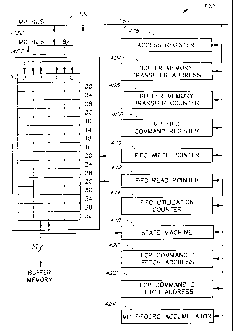
As illustrated in Figure 4, in one embodiment, the MP FIFO 302 includes a
buffer memory transfer address
register 404, a buffer memory transfer counter 406, a MP FIFO command register
408, a FIFO write pointer 410, a FIFO
read pointer 412, a FIFO utilization counter 414, the FIFO access register
416, FCP command fetch address registers 420,
422, and a state machine 418. The aforementioned registers and counters are
used to control data transfers to and from
the MP FIFO 302. The FIFO array 402 may be memory mapped directly into an
internal microcontroller register file. In one
embodiment, the registers, counters, and FIFO array 402 are accessible as
random access memory by the microprocessor
108 and/or the microcontraller 120. As discussed below, great flexibility in
accessing Fibre frames and in locating
associated CRC data located at a random FIFO location is thus provided.
In one embodiment, a semaphore is used to avoid conflict between multiple
devices, such as the microprocessor
108 and the microcontroller 120, trying to access the FIFO resources. Thus, in
one embodiment a register is used to store
a semaphore grant bit. Before attempting to use the FIFO 302, or to modify
FIFO information, such at the pointers,
counters, access register, and the like, a requesting device first attempts to
acquire the semaphore.
-7-
SUBSTITUTE SHEET (RULE 26)
CA 02370596 2001-11-02
WO 00/67107 PCT/US00/12433
The MP FIFO command register 408 is used to initiate transfers to or from the
buffer memory 112 from or to the
MP FIFO 302. A variety of FIFO commands are used to control data transfers
between the FIFO 302 and the buffer
memory 112. The transfer commands can generally be categorized in four groups.
These command groups include load
and unload commands, read and write commands, control commands, and automate
commands. Some of the commands
enable direct frame access to Fibre Channel frames. The load and unload data
transfer commands treat the FIFO 302 as a
first-in-first-out memory. The load and unload data transfer commands cause
the loading and/or unloading of the FIFO 302
using the MP FIFO write pointer 410, the MP FIFO read pointer 412, and the MP
FIFO utilization counter 414. In one
embodiment, one or more transfer commands are configured to handle transfers
greater than the FIFO size.
The read and write data transfer commands treat the FIFO as a random access
memory. In one embodiment, the
read and write commands read and write data starting at a location zero in the
FIFO 302. In another embodiment, the data
transfers may begin at other FIFO memory addresses.
The control commands, such as the Clear FIFO command, may be used to clear the
FIFO by clearing the
associated counters and registers. In addition one or more of the control
commands may be used to pause or stop any
command currently in progress. The automate commands, such as the Fetch FCP
command and the Update Current FCP
Command Pointer command, efficiently automate the fetching or transfer of
commands, such as Fibre Channel command
frames, from the buffer memory 112 or the like, to the FIFO 302. As previously
discussed, in one embodiment, the FIFO
commands are executed by a state machine.
The FIFO read and write pointers 412, 410 are respectively are used to keep
track of the current read and write
locations when the FIFO 302 is being accessed in a first-in-first-out manner.
The write pointer 410 controls the location or
address of a current FIFO write operation. The write pointer 410 contains a
byte offset relative to the starting address of
the FIFO array 402. In one embodiment, the write pointer 410 is initialized to
zero upon a power-on reset or upon receipt
of a MP DMA FIFO Reset command. Similarly, the read pointer 412 controls the
location or address of a current FIFO read
operation. The read pointer 412 contains a byte offset relative to the
starting address of the FIFO array 402. In one
embodiment, the read pointer 412 is initialized to zero upon a power-on reset
or upon receipt of a MP DMA FIFO Reset
command.
The FIFO utilization counter 414 is used to keep track of the FIFO utilization
count. For example, the FIFO
utilization counter 414 may track the amount of FIFO memory locations
utilized, and hence, the number of FIFO locations
which are not being utilized. In one embodiment, the utilization counter 414
may be read or written to as register by the
local microprocessor 108 andlor microcontroller 120. The readable count
provides the number of bytes stored in the FIFO
array 402. In one embodiment, the number of bytes is rounded down to the
nearest word boundary. The FIFO count is
decremented as data is read from the FIFO array 402. Thus, in one embodiment,
a 4 byte read operation via the access
register 416 decrements the count by four when the last of 4 byte is read.
Similarly, reading two 16 bit halfwords from
the FIFO array 402 decrements the FIFO count by four when the last 16 bit
halfword is read. In addition, the FIFO count is
decremented by four upon reading a 32 bit word from the FIFO array 402. The
data read from the array 402 may be
stored in another memory, such as the buffer memory 112.
-8-
SUBSTITUTE SHEET (RULE 26)
CA 02370596 2001-11-02
WO 00/67107 PCTIUSOO/12433
The MP FIFO access register 416 is used by the microprocessor 108 to read and
write data to the FIFO array
402. Thus, data written to the access register 416 is in turn written to the
FIFO location indicated by the write pointer
410. The write pointer 410 is typically incremented following such a write
access. Similarly, when data is read via the
access register 416, the FIFO read counter is incremented. In one embodiment,
a varying number of bytes may be read or
written via the access register 416. Thus, by example, either one byte or two
bytes may be read or written in one
operation using the access register 416. SDRAM access to the FIFO array 402 is
provided the state machine 418, as
discussed below.
The MP FIFO buffer memory transfer address register 404 is used when
transferring data to or from the buffer
memory 112. The buffer memory transfer address register 404 is loaded with the
appropriate buffer memory address
before a transfer takes place. The buffer memory transfer counter 406 is used
to keep track of the number of bytes
transferred to the buffer memory 112. The transfer counter 406 is set to a
number corresponding to the amount of data,
such as the number of bytes, to be transferred. In one embodiment, the byte
count is a multiple of four. Advantageously,
the byte count can exceed the size of the FIFO array 402. In one embodiment,
the transfer counter may be set to transfer
up to 64K bytes. In another embodiment, the transfer counter 406 can be set to
a count greater than 64K. Thus, in one
embodiment of the present invention, block transfers are not limited to the
FIFO size. If the FIFO array 402 becomes full
during a transfer of data to the FIFO 302, the transfer is then suspended
until data is read out of the FIFO array 402.
Similarly, if the FIFO array 402 becomes full during a transfer, the transfer
is then suspended until data is loaded in the
FIFO array 402.
In one embodiment, a device, such as the microprocessor 108 or the
microcontroller 120, can access the FIFO
302 through the MP FIFO access register 416 while the FIFO commands are
executing. Thus, for example, the
microprocessor or microcontroller can read from the FIFO 302 as the FIFO 302
is being filled. Similarly, the microprocessor
108 or the microcontroller 120 can write to the FIFO 302 as the FIFO is being
read or emptied.
The operation of the MP FIFO 302 as a first-in-first-out memory will now be
discussed. In one embodiment,
writing to the FIFO access register 416 causes the data to be stored at the
offset loaded into the write pointer. The write
pointer is incremented in a circular fashion each time data is written to the
FIFO access register 416. A pause signal is
generated when a write operation to the access register 416 is attempted when
the utilization counter count equals the
FIFO size. This ensures that FIFO data is not overwritten. The pause signal
causes the device writing to the FIFO 302,
such as the microprocessor 108 or the microcontroller 120, to stall until
memory locations are made available. The
memory locations may be made available by the performance of a read operation
from the access register, which would
thereby decrement the utilization count. The pause function permits data
transfers to and through the FIFO 302 to be
greater than the FIFO size. If the FIFO 302 fills or empties during a write or
read process, the process is simply paused,
rather than terminated. Thus, the pause function ensures overflow conditions
do not occur during data transfers.
In addition, the FIFO memory locations may be made available upon the
execution of a FIFO Clear command,
which would clear or zero the utilization counter.
-9-
SUBSTITUTE SHEET (RULE 26)
CA 02370596 2001-11-02
WO 00/67107 PCT/US00/12433
Reading the FIFO access register 416 causes the data located at the read
pointer offset to be read and
increments the read pointer in a circular fashion. The utilization word count
is decremented each time a read operation is
performed. The pause signal is generated if a read operation from the FIFO
access register, is attempted when the FIFO
utilization count is zero. The pause signal causes the device reading the FIFO
302, such as the microprocessor 108, the
microcontroller 120, or the DMA channel, to stall until one or more FIFO
memory locations are filled or loaded. The memory
locations may loaded by the performance of a write operation from the access
register, which would thereby increment the
utilization count. Thus, the pause function ensures underflow conditions do
not occur during data transfers.
As previously discussed, in one embodiment the MP FIFO array 402 may also be
directly and randomly accessed
by the microprocessor 108 or microcontroller 120. The static RAM elements used
to form the MP FIFO array 402 enable
the MP FIFO 302 to be read as a 64 byte random access memory. The array 402
may be mapped into both the
microprocessor address space and the microcontroller address space. In one
embodiment, reading or writing the MP FIFO
302 as a directly addressable random access array does not affect the MP FIFO
registers or counters associated with the
first-in=first=out type of operation.
The MP FIFO 302 may also be used for storing microprocessor or microcontroller
internal register information
during context switching operations. Thus, the microprocessor 108 or
microcontroiler 120 can quickly swap register file
data in and out of the FIFO array 402. The efficient register swapping
provided by one embodiment of the present
invention advantageously allows the processor to quickly switch tasks.
Context switching allows for disk controller tasks to be performed in a more
efficient manner. For example, if,
while transferring data from the disk 106 to the Fibre Channel interface 124
using one or more the disk controller
processors, such as the microcontroller 120, the transfer outpaces the disk's
ability to supply data, it would be more
efficient for the microcontroller to perform some other task during this
period, rather than wastefully pausing until the disk
106 catches up. By way of example, it would be advantageous to send cache data
to a different host, while waiting for
additional disk data to accrue. Thus, one embodiment of the present invention
allows the context of one operation to be
saved in the FIFO 302 while another task is performed. Context switching can
be performed especially quickly with one
embodiment of the present invention, as the FIFO array 402 is accessible as an
internal register file of the microcontroller
120. The microcontroller 120 can therefore quickly swap context information
into and out of the FIFO array 402. Thus,
the context does not have to be stored in slower secondary memory, such as the
buffer memory 112. Depending on the
size of the FIFO array 402 and the amount of context data, the FIFO array 402
may be used to store multiple contexts at
the same time.
The context information may include relevant information used to keep track of
a task, such as frame counts,
sequence counts, transfer counts, and the like. Thus, in one embodiment, if a
transfer runs out of available data, the
transfer operation may be suspended, and the context of the operation may be
stored in the FIFO 402. Depending on the
size of the cache data, the context may be changed several times.
The stored context may be restored using a variety of techniques. For example,
the stored context may be
restored once additional data is available for the suspended transfer. The
restored context can overwrite an existing
-10=
SUBSTITUTE SHEET (RULE 26)
CA 02370596 2001-11-02
WO 00/67107 PCTIUSOO/12433
context, if no longer needed. Using another technique, a context can be
swapped back into FIFO 402, and the replaced
context can be swapped out of the FIFO 402 at the same time.
Referring to Figure 3, an SDRAM controller 304 and an arbiter module 306 are
used in accessing the buffer
memory 112. The arbiter 306 selects a requester when multiple requests are
active, and establishes an access tenure.
The arbiter 306 then grants the requester an access turn. The SDRAM controller
304 then proceeds to move data
between the buffer memory 112 and the buffer controller data bus.
As previously discussed, special commands are provided to facilitate access to
the data stored in the MP FIFO
302. In one embodiment, the FIFO state machine 418 accepts and performs the
commands, listed in Table 2 below.
In one embodiment, a transfer is initiated upon writing a command to the
command register 408. A MP DMA
FIFO Command Active bit is set in a status register to indicate that a FIFO
command is in the process of being executed.
Table 1 below illustrates one embodiment of the bit assignment for the command
register 408.
Bit Position Name
15-8 Reserved
7 Interrupt When Complete
6 Select FCP CMD 2
5 Swap Halfword In Words
4 Swap Bytes in Halfwords
3-0 Command
Table 1
Referring to Table 1, bits 15-8 of the command register 408 are reserved. When
the LBA (logical block address)
format bit (8) is set, a CRC hardware accumulator is initialized with the
inverted LBA as the seed. Otherwise the CRC
accumulator will just use the seed, which, in one embodiment, is all ones. In
one embodiment, the use of a dedicated,
hardware CRC accumulator permits the CRC to be quickly calculated without
loading down the processors with this task.
Commands loaded into the command register 408 may cause an interrupt signal to
be generated. In one
embodiment, an interrupt is generated when a command is completed and the
Interrupt When Complete bit (7) is set in the
command register 408. A Command Active bit is set in the status register while
a command is still active. In addition, a
Command Complete bit may be set in the status register upon completion of a
command. In one embodiment, the interrupt
may go to a processor, such as the microcontroller 120 or microprocessor 108.
The receiving processor may mask the
interrupt, or pass the interrupt on to another processor or to the host 104.
A description of bits 6-4 will be later described. Table 2, below, illustrates
the operations defined by bits 3-0 of
the command register 408.
-11-
SUBSTITUTE SHEET (RULE 26)
CA 02370596 2001-11-02
WO 00/67107 PCT/US00/12433
Operation
Clear FIFO
Stop FIFO
Load FIFO
Unload FIFO
Load FIFO with BCRC check
Unload FIFO with BCRC Generation
Read from Buffer Memory
Write to Buffer Memory
Fetch FCP Command
Update Current FCP Command pointer
Table 2
The Clear FIFO command sets or clears the FIFO read and write pointers 412,
410 to zero. In one embodiment,
the contents of the FIFO array 402 are unaltered by the Clear FIFO command. In
one embodiment, the Clear FIFO
command may be issued while other commands are active.
The Stop FIFO command stops any active FIFO command and resets the FIFO state
machine 418. In one
embodiment, the Stop FIFO command may be issued while other commands are
active. In one embodiment, the contents of
the pointers 410, 412 and the FIFO array 402 are unaltered by the Stop FIFO
command.
The Load FIFO command transfers data from the buffer memory 112 to the MP FIFO
302. The data is loaded
into the FIFO array 402 starting at the location defined by the MP FIFO write
pointer 410. The number of bytes to be
transferred is set in the Buffer Memory transfer counter 406. The buffer
memory start address for the transfer is set in
the buffer transfer address register 404. Advantageously, the number of bytes
to be transferred is allowed to exceed the
size of the FIFO array 402. Thus, transfers can be of any desired size. In one
embodiment, the transfer counter is sized to
manage transfers up to 4 Kbytes in size, as compared to the 64 byte FIFO array
size. However, the transfer counter can
be sized to handle larger or smaller transfers, as desired.
In one embodiment, 4 Kbytes may be transferred as a result of one Load
command. The Load FIFO operation will
be suspended if the FIFO 302 is full and the transfer is incomplete. An MP DMA
FIFO Full bit is set in the status register is
set to indicate the FIFO array 402 is full. The transfer may resume
automatically when the FIFO 302 begins to empty and
the MP DMA FIFO Full bit is cleared.
Figure 8 illustrates one example of a Load FIFO command operation. The FIFO
array 402 is assumed to contain
"don't care" information, designated by "xx". The write pointer (WP) 410 and
read pointer (RP) 412 are set to "0," thereby
pointing to the physical beginning address of the FIFO array 402. When the
read pointer 412 points to the same address as
the write pointer 410, the FIFO 402 is either empty or full, depending on the
utilization count. The FIFO word count,
-12-
SUBSTITUTE SHEET (RULE 26)
CA 02370596 2001-11-02
WO 00/67107 PCTIUSOO/12433
indicating how many FIFO word locations have been used, is at "0," indicating
the FIFO 402 is empty. The Buffer Memory
transfer counter 406 is loaded with "32", indicating 32 bytes are to be
transferred from the buffer memory 112 to the
FIFO array 402. For clarity, in the present example, the buffer memory 112 is
loaded with sequential numbers, though, in
one embodiment, the actual buffer memory contents does not affect the
operation of the Load FIFO command.
Once the Load FIFO command is received by the command register 408, the
transfer of 32 bytes from the buffer
memory 112 to the FIFO array 402 takes place. The buffer memory data is
written to the FIFO 302 beginning at the
location indicated by the write pointer 410, in this example "0". The write
pointer 410 is incremented as each byte is
transferred and loaded into the FIFO array 402. This process repeats until the
number of bytes specified by the transfer
count, in this example 32, is transferred. As illustrated in Figure 8, once
the Load FIFO command is complete, the FIFO
array 402 contains the transferred data, the write pointer 410 has been
incremented to 32, the read pointer 412 remains
at 0, and the FIFO word count is at 8. In one embodiment, the transferred data
also remains in the buffer memory 112.
The Unload FIFO command transfers data from the MP FIFO 302 to the buffer
memory 112. The data is
unloaded from the FIFO array 402 starting at the location defined by the MP
FIFO read pointer 412. The number of bytes
to be transferred is set in the Buffer Memory transfer counter 406. The buffer
memory start destination address for the
transfer is set in the buffer transfer address register 404. As with the Load
command, the number of bytes to be
transferred is allowed to exceed the size of the FIFO array 402. The Unload
FIFO operation will be suspended if the FIFO
302 is empty and the transfer is incomplete. An MP DMA FIFO Not Empty bit is
cleared in the status register is set to
indicate the FIFO array 402 is empty. The transfer may resume when the FIFO
302 begins to fill and the MP DMA FIFO
Not Empty bit is set.
Figure 9 illustrates one example of an Unload FIFO command operation. The
write pointer (WP) 410 is currently
set to "32" and the read pointer (RP) 412 is set to "0". The FIFO word count,
indicating how many FIFO word locations
have been used, is at "8," indicating that there are 8 words in the FIFO array
402. The Buffer Memory transfer counter
406 is loaded with "32", indicating 32 bytes are to be transferred from the
FIFO array 402 to the buffer memory 112. For
clarity, in the present example, the FIFO array 402 is loaded with sequential
numbers, though the actual buffer memory
contents does not affect the operation of the Unload FIFO command.
Once the Unload FIFO command is received by the command register 408, the
transfer of 32 bytes from the FIFO
array 402 to the buffer memory 112 takes place. The data is read out of the
FIFO 302 beginning at the location indicated
by the read pointer 412, in this example "0". The read pointer 412 is
incremented by 4 as each word is transferred and
loaded into the buffer memory 112. This process repeats until the number of
bytes specified by the transfer count, in this
example 32, is transferred. As illustrated in Figure 9, once the Unload FIFO
command is complete, the buffer memory 112
contains the transferred data, the write pointer 410 remains at 32, the read
pointer 412 is has been incremented to 32,
and the FIFO word count is at 0, indicating that the FIFO is empty. In one
embodiment, even though the FIFO array 402 is
empty, the data has not been erased from the FIFO array 402.
The Load FIFO with BCRC (Block CRC) Check command transfers data from the
buffer memory 112 to the MP
FIFO 302 while performing a CRC check. This command is especially useful for
transferring disk sectors with associated
-13-
SUBSTITUTE SHEET (RULE 26)
CA 02370596 2001-11-02
WO 00/67107 PCTIUSOO/12433
sector CRCs. The data is loaded into the FIFO array 402 starting at the
location defined by the MP FIFO write pointer 410.
The number of bytes to be transferred is set in the Buffer Memory transfer
counter 406. The buffer memory start source
address for the transfer is set in the buffer transfer address register 404.
The number of bytes to be transferred is allowed
to exceed the size of the FIFO array 402. The Block CRC, which in one
embodiment is the last word to be transferred, is
checked. If the CRC check indicates that the Block CRC is valid, an MP DMA
FIFO CRC Good bit is set in the status
register. The Load FIFO with BCRC Check operation will be suspended or paused
if the FIFO 302 is full and the transfer is
incomplete. The transfer may resume automatically when the FIFO 302 begins to
empty.
The pause feature is particularly advantageous for transferring large data
blocks greater is size than the FIFO
302, with an associated error detection and/or correction code, from the
buffer memory 112. The error detection code
may be, by way of example, a CRC. Using conventional techniques, the transfer
of data blocks larger than the FIFO array
402 may be disadvantageously performed by treating the large block as several
smaller blocks, equal in size to the FIFO
array 402. Thus, the large block would be transferred as a series of smaller,
separate, transfers. However, this
conventional technique can make the calculation of the CRC, which is for the
entire block, difficult or slow to perform by
requiring reseeding of the CRC accumulator at the start of each FIFO-sized
transfer. In contrast, one embodiment of the
present invention permits the entire block to be treated as one block, with
the CRC accumulated over the course of the
transfer, without reseeding.
Figure 10 illustrates one example of a Load FIFO with BCRC Check command
operation. The FIFO array 402 is
assumed to contain "don't care" information, designated by "xx". The write
pointer (WP) 410 and read pointer (RP) 412
are set to "0," thereby pointing to the physical beginning address of the FIFO
array 402. The FIFO utilization word count is
at "0," indicating the FIFO array 402 is empty. The Buffer Memory transfer
counter 406 is loaded with "32+4" or 36,
indicating 36 bytes, including 32 data bytes and 4 BCRC bytes, are to be
transferred from the buffer memory 112 to the
FIFO array 402. For clarity, in the present example, the buffer memory 112 is
loaded with sequential numbers, though, in
one embodiment, the actual buffer memory contents does not affect the
operation of the Load FIFO with BCRC Check
command.
Once the Load FIFO with BCRC Check command is received by the command register
408, the transfer of 32
data bytes and 4 BCRC bytes from the buffer memory 112 to the FIFO array 402
takes place. The buffer memory data
and BCRC is written to the FIFO 302 beginning at the location indicated by the
write pointer 410, in this example "0". The
write pointer 410 is incremented as each byte is transferred and loaded into
the FIFO array 402. This process repeats until
the number of bytes specified by the transfer count, in this example 36, is
transferred. The BCRC is checked during the
transfer, and if the CRC check indicates that the CRC is valid, the MP DMA
FIFO CRC Good bit is set in the status register.
As illustrated in Figure 10, once the Load FIFO with BCRC Check command is
complete, the FIFO array 402 contains the
transferred data, the write pointer 410 has been incremented to 36, the read
pointer 412 remains at 0, and the FIFO word
count is at 9. In one embodiment, the transferred data also remains in the
buffer memory 112.
The Unload FIFO with BCRC Generation command transfers data from the MP FIFO
302 to the buffer memory
112 while generating a Block CRC. The transfer begins starting at the location
defined by the MP FIFO read pointer 412.
-14-
SUBSTITUTE SHEET (RULE 26)
CA 02370596 2001-11-02
WO 00/67107 PCTIUSOO/12433
The number of bytes to be transferred is set in the Buffer Memory transfer
counter 406. The buffer memory start
destination address for the transfer is set in the buffer transfer address
register 404. The last word to be transferred is a
dummy word and is replaced with a block CRC calculated by the CRC engine 132.
The number of bytes to be transferred
is allowed to exceed the size of the FIFO array 402. The Unload FIFO with BCRC
Generation operation will be suspended
or paused if the FIFO 302 is empty and the transfer is incomplete. The
transfer may resume automatically when the FIFO
302 begins to fill.
Figure 11 illustrates one example of an Unload FIFO with BCRC Generation
command operation. The buffer
memory 112 is assumed to contain "don't care" information, designated by "xx".
For clarity, in the present example, the
FIFO array 402 is loaded with 32 bytes of sequential numbers. In addition, the
4 bytes following the data "contain" a
dummy BCRC. That is, the BCRC for the 32 data bytes at FIFO addresses 0-31 has
not been calculated yet, but for FIFO
management purposes, the write pointer 410 is set to 36, as if address
locations 32-35 contained an actual BCRC. The
read pointer (RP) 412 is set to "0". The FIFO utilization word count,
indicating how many FIFO word locations have been
used, is at "9," indicating that there are 9 words in the FIFO array 402. The
Buffer Memory transfer counter 406 is loaded
with "32+4," or 36, indicating 36 bytes are to be transferred from the FIFO
array 402 to the buffer memory 112.
Once the Unload FIFO with BCRC Generation command is received by the command
register 408, the transfer of
32 bytes from the FIFO array 402 to the buffer memory 112 takes place. The
data is read out of the FIFO 302 beginning
at the location indicated by the read pointer 412, in this example "0". The
read pointer 412 is incremented as each word is
transferred and loaded into the buffer memory 112. The BCRC is continuously
calculated during this transfer. This
process repeats until the number of bytes specified by the transfer count,,
minus the 4 bytes for the BCRC data, is
transferred. In this example, 32 bytes are transferred from the array 402. The
last 4 bytes transferred to the buffer
memory 112 contains the BCRC data, supplied by the CRC accumulator rather than
the FIFO array 402. As illustrated in
Figure 11, once the Unload FIFO with BCRC Generation command is complete, the
buffer memory 112 contains the
transferred data with the associated BCRC. The write pointer 410 remains at
36, the read pointer 412 has been
incremented to 36, and the FIFO word count is at 0, indicating that the FIFO
is empty. In one embodiment, even though the
FIFO array 402 is empty, the data has not been erased from the FIFO array 402.
The Read from Buffer Memory command transfers data 64 bytes of data from the
buffer memory 112 to the MP
FIFO 302. The data is loaded into the FIFO array 402 starting at the beginning
or zero address of the FIFO array 402. The
buffer memory start source address for the transfer is set in the buffer
transfer address register 404. In one embodiment,
the read pointer 412 and the transfer counter 406 are automatically
initialized using default values. Thus, rather than
having to go through a lengthy setup process, one command quickly initializes
the counters. In addition, in one
embodiment, no CRC check is performed. Thus, the Read from Buffer Memory
command, which automatically loads 64
bytes at the start of the FIFO array 302, allows sequential pages to be
quickly loaded without having the overhead time
associated with managing the FIFO pointers. This command permits a processor,
such as the microprocessor 108 or the
microcontroller 120, to quickly perform FIFO loads to examine data stored in
the buffer memory at 64 byte intervals. In
one embodiment, no CRC is performed during this transfer.
-15-
SUBSTITUTE SHEET (RULE 26)
CA 02370596 2001-11-02
WO 00/67107 PCT/US00/12433
Figure 13 illustrates one example of a Read from Buffer Memory command
operation. The FIFO array 402 is
assumed to contain "don't care" information, designated by "xx". The write
pointer (WP) 410, read pointer (RP) 412,
transfer counter 406, and word count, based on the utilization counter 414,
are automatically initialized with default
values. For clarity, in the present example, the buffer memory 112 is loaded
with sequential numbers, though, in one
embodiment, the actual buffer memory contents does not affect the operation of
the Read from Buffer Memory command.
Once the Read from Buffer Memory command is received by the command register
408, the automatic transfer
of 64 bytes from the buffer memory 112 to the FIFO array 402 takes place. The
buffer memory data is written to the
FIFO array 402 beginning at first FIFO memory location. All 64 bytes are
transferred. As illustrated in Figure 13, once the
Read from Buffer Memory command is complete, the FIFO array 402 contains the
transferred data. In one embodiment,
the transferred data also remains in the buffer memory 112.
The Write to Buffer Memory command transfers the entire 64 byte content of the
FIFO array 402 to the buffer
memory 112. The data is loaded into the FIFO array 402 starting at the
beginning or zero address of the FIFO array 402.
The buffer memory start destination address for the transfer is set in the
buffer transfer address register 404. In one
embodiment, the Write to Buffer Memory command does not use the write pointer
410, the read pointer 412, or the
transfer counter 406. Thus, the Write from Buffer Memory command, which
automatically unloads 64 bytes at the start
of the FIFO array 302, allows sequential pages to be quickly transferred to
the buffer memory 112 without having the
overhead time associated with managing the FIFO pointers. In one embodiment,
no CRC is performed during these
transfers.
Figure 14 illustrates one example of a Write to Buffer Memory command
operation. The buffer memory 112 is
assumed to contain "don't care" information, designated by "xx". The write
pointer (WP) 410, read pointer (RP) 412,
transfer counter 406, and utilization counter 414 are automatically
initialized to default values. For clarity, in the present
example, the FIFO array 402 is loaded with sequential numbers, though, in one
embodiment, the actual contents do not
affect the operation of the Write to Buffer Memory command.
Once the Write to Buffer Memory command is received by the command register
408, the automatic transfer of
64 bytes from the FIFO array 402 to the buffer memory 112 takes place. The 64
bytes of FIFO data is automatically
written to the buffer memory 112 beginning at the address stored in the buffer
transfer address register 404. As
illustrated in Figure 14, once the Write to Buffer Memory command is complete,
the buffer memory 112 contains the
transferred data, and the write pointer 410 and the read pointer 412 are
unaltered. In one embodiment, the transferred
data also remains in the FIFO array 402.
The Select FCP (Fibre Channel Protocol) CMD 2 bit (6) is used in conjunction
with the Fetch Current FCP
command and the Update Current FCP Command Pointer command. When the Fetch
Current FCP command is executed,
the current FCP command is transferred from the command buffer in the buffer
memory 112 to the MP FIFO array 402. In
one embodiment, this transfer is performed automatically, without processor
intervention, once the FIFO command is
written to the command register 408.
=16=
SUBSTITUTE SHEET (RULE 26)
CA 02370596 2001-11-02
WO 00/67107 PCT/USOO/12433
As discussed in greater detail below, the state machine 418 executes the Fetch
Current FCP command by
executing a Clear FIFO sequence, clearing the pointers and utilization
counter, and then copying the FCP Command Fetch
Address to the MP FIFO buffer memory transfer address register 404. The Select
FCP CMD 2 bit (6) determines which of
the two fetch addresses, FCP Command 1 Fetch Address or FCP Command 2 Fetch
Address, will be used to fetch the
current FCP command. The provision of two fetch addresses, FCP Command 1 Fetch
Address or FCP Command 2 Fetch
Address, advantageously allow two command buffers to be present in the buffer
memory 112. The FCP Command 1 Fetch
Address and FCP Command 2 Fetch Address are correspondingly stored in the FCP
Command 1 Fetch Address register 420
and the FCP Command 2 Fetch Address register 422. The registers 420, 422
contain the corresponding FCP Command
Frame Table base, FCP Command fetch address frame pointer, and 64 byte command
frame start.
The state machine 418 then sets the MP FIFO buffer memory transfer counter 406
to 60, which is the size, in
bytes, of an FCP command, excluding the associated CRC and buffer length
field. The buffer length field is loaded into the
MP FIFO 302 beginning at the top, or zero address location, of the FIFO array
402. Thus, the buffer length field may be
quickly and automatically located for use by processing elements, such as the
microcontroller 120. In one embodiment, the
buffer length field is at a fixed location or spacing relative to the FCP
command header. The buffer length field may be
used to locate the CRC, which is checked to determine if the frame is
corrupted. In one embodiment, the FCP command
frame is stored in the buffer memory 112 with the CRC located above the buffer
length field, as illustrated in Figure 7. A
Load FIFO with BCRC Check command is then automatically executed. In one
embodiment, the Interruption Upon Complete
bit is set as well.
Thus, by having the state machine automatically perform the complex task of
reading in and checking an FCP
command without requiring further microprocessor or microcontroller
intervention, the processing burden of the
microprocessor 108 and the microcontroller 120 is greatly reduced. In
addition, the reading of the FCP command is
accomplished more quickly and efficiently.
The Update Current FCP Command Pointer command performs the steps needed to
advance a Current Command
Fetch address counter or register. First, the Fetch Address pointer is
incremented by the command size, which is 64. The
Select FCP CMD 2 bit (6) determines which of the FCP Command 1 Fetch Address
and FCP Command 2 Fetch Address will
be used. The MP FIFO command complete interrupt is then generated. The Command
count is then decremented.
Figure 12 illustrates one example of a Fetch Current FCP command operation.
The FIFO array 402 is assumed to
contain "don't care" information, designated by "xx". The write pointer (WP)
410, read pointer (RP) 412, and word count
are also "don't cares." The buffer memory 112 is loaded with an FCP Command
frame, including 6 words for the frame
header, 8 words for the frame payload, 1 word for the FCP Command CRC, and a 1
word buffer length field, for a total of
64 bytes.
Once the Fetch Current FCP command is received by the command register 408,
the automatic transfer of 64
bytes from the buffer memory 112 to the FIFO array 402 takes place. The
transfer is from the buffer memory location
indicated by the corresponding FCP Command Fetch Address. First, the buffer
length field is automatically loaded at the
beginning or top address of the FIFO array 402. Thus, the buffer length field
will be the first word later unloaded from the
-17-
SUBSTITUTE SHEET (RULE 26)
CA 02370596 2001-11-02
WO 00/67107 PCT/US00/12433
FIFO array 402. The FCP Command Frame header is then transferred, followed by
the frame payload and the CRC, which
is checked. As illustrated in Figure 12, once the Fetch Current FCP command is
complete, the FIFO array 402 contains the
transferred data, with the buffer length field on top. The write pointer 410
and the read pointer 412 remain at 0, and the
FIFO word count is at 64, indicating the FIFO array 402 is full.
Figure 15 illustrates one embodiment of a context switching operation. This
example illustrates swapping or
transferring a context previously stored in the FIFO array 402 to an exemplary
register file, while transferring the context
from the register file to the FIFO array 402. The register file may be one of
any number of register files, and may be used
to contain a variety of data or contexts, such as an FCP header, a transfer
count status, and so on. In the present
example, the FIFO array 402 contains a first context stored in the first 28
bytes of the array. The remainder of the array
402 is assumed to contain "don't care" information, designated by "xx". The
write pointer (WP) 410 is at 28, that is, the
write pointer 410 will cause the next data received by the FIFO array 402 to
be written in the memory location following
the first context. The read pointer (RP) 412 is set to "0," thereby pointing
to the physical beginning address of the FIFO
array 402. The FIFO utilization word count, indicating how many FIFO word
locations have been used, is at "7." The
microcontroller (MC) accumulator is set to "14." The Buffer Memory transfer
counter 406 is a "don't care," as data is not
being transferred to or from the buffer memory 112 in this operation. The
register file 1502 contains a second context,
including 28 bytes. While, in this example, the first and second contexts are
the same size, they could have different sizes
as well. For clarity, in the present example, the FIFO array 402 is loaded
with sequential numbers 00-1B, while the register
file 1502 is loaded with sequential numbers 20-3B.
An MC Exchange Load FIFO command is used to perform context switching or
swapping. Once an MC
EXCHANGE Load FIFO command is issued, the context stored in the FIFO array 402
is swapped with the context stored in
the register file 1502. In the illustrated example, the first context is
swapped out, but also is not erased from the FIFO
array 402. However, if desired, the first context could be overwritten in the
FIFO array 402 during a swap operation, while
the swapped out copy of the first context would be stored in the register file
1502. For example, if the context being
swapped in was larger than the unused FIFO locations, all or part of the first
context stored in the FIFO array 402 may be
overwritten. Thus, in one embodiment, if the context being swapped in from the
register file is 64 bytes, the first context
in the FIFO array 402 would be completely overwritten.
As illustrated in Figure 15, in this example, the context transferred from the
register file 1502 to the FIFO array
402 is stored immediately after the first context. The register file 1502 now
contains the first context. The write pointer
(WP) 410 has advanced to 56, reflecting the additional data written to the
FIFO array 402. The read pointer (RP) 412 has
advanced to 28, reflecting the fact that 28 bytes have been read from the
array 402. The FIFO word count remains at 7,
as the same number of words were read out of the array 402 as were written to
the array 402 during the swap.
One embodiment of the present invention optionally performs data translation
when data is transferred between
the MP FIFO 302 and the buffer memory 112. As illustrated in Figure 6, two 16
bit halfwords within a 32 bit word may be
swapped, and two bytes within each halfword may be swapped. Bit 5 of the
command register 408 is used to cause the
halfwords within a word to be swapped. Bit 4 is used to cause bytes within
halfwords to be swapped. These swapping
-18-
SUBSTITUTE SHEET (RULE 26)
CA 02370596 2001-11-02
WO 00/67107 PCT/US00/12433
functions advantageously allow data formatted in a big-endian format to be
converted to a little endian format. Similarly,
these swapping functions advantageously allow data formatted in a little-
endian format to be converted to a big-endian
format. For example, Fibre Channel conventionally uses the little-endian
format, while the processors 106, 120 may use
the big-endian format. In addition, the swapping function allows words
transferred in or out of the FIFO 302 to be
realigned on different boundaries.
Additional command information, including, buffer memory access direction,
transfer count values, the source of
buffer memory addresses, and comments, is provided in Table 3, below:
COMMAND BUFFER TRANSFER BUFFER COMMENTS
MEMORY COUNT MEMORY
ACCESS ADDRESS
DIRECTION
NO OPERATION NONE 0 N/A
CLEAR FIFO NONE 0 N/A CLEAR FIFO READIWRITE
POINTERS & UTILIZATION
COUNTER
STOP FIFO NONE 0 N/A FORCE STATE MACHINE TO
IDLE STATE
LOAD FIFO READ XFER CNT BUFFER XFER
REG ADDR
UNLOAD FIFO WRITE XFER CNT BUFFER XFER
REG ADDR
LOAD FIFO W READ XFER CNT BUFFER XFER CHECK CRC WHILE LOADING
BCRC REG ADDR FIFO
UNLOAD FIFO WRITE XFER CNT BUFFER XFER GENERATE CRC WHILE
W BCRC REG ADDR UNLOADING FIFO
READ WRITE 64 BUFFER XFER
ADDR
WRITE WRITE 64 BUFFER XFER
ADDR
FETCH FCP READ 64 FCP FETCH CHECK CRC
COMMAND ADDR PTR
UPDATE FCP NONE 0 N/A UPDATE FCP ADDRESS AND
POINTERS COUNT & CLEAR COMMAND
COMPLETE INTERRUPT
Table 3
In one embodiment, one or more of the commands listed above may be issued
while another command is
executing. For example, in one embodiment, the No Operation (NOP), the Clear
FIFO, and the Stop FIFO commands can be
issued while other commands are being executed.
The state machine 418 controls controller memory access resources, including
the MP FIFO pointers, the MP
FIFO buffer memory transfer counter 406, the Fibre Channel protocol (FCP)
fetch address counters, the CRC accumulators,
and the frame length counter. The state machine 418 can initialize these
resources, set modes, and acts as the SDRAM
requestor.
-19-
SUBSTITUTE SHEET (RULE 26)
CA 02370596 2001-11-02
WO 00/67107 PCTIUSOO/12433
Figures 5A-D illustrate one embodiment of the MP FIFO state machine 418.
Beginning at an Idle state 514,
upon receipt of an Unload FIFO command, the state machine 418 proceeds to
state 502, whereupon the process of
unloading the FIFO 302 begins. If the FIFO 302 is not empty, the state machine
418 proceeds to state 504. The FIFO
302 is then continuously unloaded until only one word remains in the FIFO
array 402 and the transfer count equals 1.
The state machine 418 then proceeds to a state 506 where the last FIFO word is
unloaded. Thus, when both
acknowledge (ACK) signal from the MP FIFO arbiter and the data acknowledge
(DACK) signal from the SDRAM
controller active, then the last piece of data in the FIFO array 402 is
transferred. The transfer count is set to 0 and
the state machine 418 returns to the Idle state 514.
If an Unload FIFO with CRC command is received while in the Idle state 514,
the state machine 418
proceeds to a state 508. The Unload FIFO with CRC command is used to write
data from the FIFO array 402 to the
buffer memory 112 while generating an associated CRC. In one embodiment, the
CRC will be the last word written to
the buffer memory 112. If the FIFO array 402 is empty, the state machine 418
remains in the Unload FIFO state 508.
However, if the FIFO array 402 is not empty, the state machine 418 proceeds to
a Unload FIFO state 510. The CRC
calculation is performed as the FIFO array 402 is being unloaded and written
into the SDRAM buffer memory. When
the transfer count equals 1, the state machine 418 proceeds to an Unload FIFO
state 512. When the CRC calculation
is complete, the CRC data is transferred to the SDRAM buffer memory 112, and
the transfer count is set to 0. The
state machine 418 then proceeds back to the Idle state 514.
If the state machine 418 receives a Load FIFO command, then the state machine
418 proceeds from Idle
state 514 to a Load FIFO state 516. The Load FIFO command is used to read data
from the buffer memory into the
FIFO array 402. If the state machine 418 is not full, then the state machine
418 proceeds to state 518 upon receipt
of an MP FIFO acknowledge signal from the arbiter. The state machine 418 then
causes data to be transferred from
the buffer memory to 112 the FIFO array 402 until the transfer count is equal
to 1, and the MP FIFO 302 generates
an almost full signal. If the transfer count is equal to 1 and the FIFO array
402 is almost full, meaning that there is
room for only one more data word, the state machine 418 proceeds to a Load
FIFO state to 520. If the transfer
counter is equal to 1, and the MP FIFO 302 generates a full signal, then upon
receipt of an MP FIFO acknowledge
signal from the arbiter and a DACK signal from the SORAM controller, the last
word is loaded into the FIFO array 402,
and the state machine 418 proceeds back to the Idle state 514.
Upon receipt of a Load FIFO With CRC command, the state machine 418 proceeds
to a Load FIFO with CRC
state 522. The Load FIFO With CRC command is used to read data from the buffer
memory 112, while checking the
CRC. In one embodiment, the CRC is the last word to be transferred. At the
state 522, if the MP FIFO 302 is not full,
the MP FIFO read signal is activated, as is an MP FIFO CRC enable signal. Upon
receipt of an MP FIFO acknowledge
signal, the state machine 418 proceeds to a Load FIFO With CRC state 524. The
state machine 418 proceeds to load
data from the SDRAM buffer memory 112 into the FIFO array 402 until an almost
full signal is asserted and the
transfer count is greater than one. During this period, the CRC is calculated.
The state machine 418 then proceeds to
=20-
SUBSTITUTE SHEET (RULE 26)
CA 02370596 2001-11-02
WO 00/67107 PCT/US00/12433
a load FIFO state with CRC 526. The state machine 418 causes the CRC to be
loaded into the FIFO array 402. The
transfer count is set to one, and the state machine 418 proceeds back to Idle
state 514.
Upon receiving a Write to Buffer Memory command, the state machine 418
proceeds from the Idle state 514
to the Write state 528. As previously described, the Write to Buffer Memory
command is used to write data from the
FIFO array 402 to the buffer memory 112. If the FIFO array 402 is not empty,
the state machine 418 proceeds to a
state 530 upon receipt of an acknowledge signal from the MP FIFO arbiter. The
FIFO array 402 is then unloaded, and
the unloaded data is written to the buffer memory 112. The FIFO unloading
process continues until only one word
remains in the FIFO memory and the transfer count equals one. The state
machine 418 then proceeds to a state 532
where the last FIFO word is unloaded. Then, when both acknowledge (ACK) signal
from the MP FIFO arbiter and the
data acknowledge (DACK) signal from the SDRAM controller active, the last
piece of data in the FIFO is transferred.
The transfer count is set to 0 and the state machine 418 returns to the Idle
state 514.
Upon receiving an Update FCP Pointers command, the state machine 418 proceeds
from the Idle state 514
to the FCMD PTR state 528. A Command Pointer Increment signal is activated for
one clock which updates the FCP
address and count. The state machine 418 the proceeds to state 536 and clears
the Command Complete interrupt.
The state machine 418 then returns to the Idle state 514.
Upon receiving a Read Buffer Memory command, the state machine 418 proceeds
from the Idle state 514 to
a Read state 538 and asserts an SDRAM read signal. If the FIFO is not full,
the state machine 418 proceeds to a
state 540 upon receipt of an acknowledge signal from the MP FIFO arbiter. Data
is then read from the buffer memory
112 into the FIFO array 402. The read process continues until the FIFO memory
is almost full and the transfer count
equals 1. The state machine 418 then proceeds to a state 542 where one more
word is read from the buffer memory
112 into the FIFO. Then, when both acknowledge (ACK) signal from the MP FIFO
arbiter and the data acknowledge
(DACK) signal from the SDRAM controller are active, the transfer count is set
to 0 and the state machine 418 returns
to the Idle state 514.
Upon receiving a Fetch FCP command, the state machine 418 proceeds from the
Idle state 514 to a FCP
Command state 544. The state machine appropriately sets the FCP_CMD, RD_SIG,
LD_CMD_LEN_ADR, CLR_FIFO,
LD_XFER_CNT_64, and REQ_SIG, signals to prepare to get the packet length data
located at the end of the packet.
Thus, the transfer address is loaded with the frame length address. In one
embodiment, the frame length address
includes a base address added to a segment size. Proceeding to a state 546,
the frame length data is retrieved. When
both acknowledge (ACK) signal from the MP FIFO arbiter and the data
acknowledge (DACK) signal from the SDRAM
controller active, the frame length is placed in the FIFO array 402.
Proceeding to a state 548, the CRC seed is reset
and the transfer address is set to the start address, or base address, of the
FCP command frame. When the
acknowledge signal drops, the state machine proceeds to a state 550. The
transfer of the packet from the buffer
memory 112 begins, and the CRC accumulation begins. The transfer continues
until the transfer count is equal to
one. The state machine 418 then proceeds to a state 552, and the last word is
transferred. The transfer counter is
now equal to zero, and the state machine proceeds to the idle state 514.
-21 =
SUBSTITUTE SHEET (RULE 26)
CA 02370596 2001-11-02
WO 00/67107 PCT/USOO/12433
While certain preferred embodiments of the invention have been described,
these embodiments have been
presented by way of example only, and are not intended to limit the scope of
the present invention. Accordingly, the
breadth and scope of the present invention should be defined only in
accordance with the following claims and their
equivalents.
-22-
SUBSTITUTE SHEET (RULE 26)