Note : Les descriptions sont présentées dans la langue officielle dans laquelle elles ont été soumises.
CA 02374794 2004-12-30
70828-27
1
TITLE OF THE INVENTION
DIVIDED-VOLTAGE FET POWER AMPLIFIERS
BACKGROUND OF THE INVENTION
Field of the Invention
The present invention relates generally to apparatus and method for power
amplifying radio frequency (rf) or microwave rf signals. More particularly,
the
present invention pertains to an rf power amplifier in which two or more field-
effect devices with selectively chosen DC bias circuits and rf decoupling
circuits
dividingly share a supply voltage, and a single rf output, two or more rf
outputs, or
two or more variably phase shifted rf outputs are produced.
Description of the Related Art
Gallium arsenide field-effect transistors (GaAsFETs) are the primary,solid-
state devices used for amplification of high frequency signals in the range of
3 GHz and higher. GaAsFETs have the advantages of being readily available and
relatively inexpensive. However, a major disadvantage of GaAsFETs is that the
maximum operating voltage is commonly +10.0 volts dc.
For many transmitter/amplifier applications, particularly airborne
applications, the do supply voltage is 28 volts dc, plus or minus 4.0 volts
dc.
Since gallium arsenide FETs have an operative voltage of +10 volts dc,~the use
of
gallium arsenide FETs has presented a problem.
Traditionally, there have been two solutions to this problem. One is to
use a linear voltage regulator. The other is to use a switching regulator.
In linear voltage regulators, the voltage is linearly regulated from the
supply of 28 volts to approximately 10 volts with the power difference being
dissipated in heat by the regulator. This type of regulation has the
disadvantages of
excessive heat and low power efficiency.
Switching regulators, on the other hand, are power converters that transfer
the power of a higher voltage supply to lower voltage with increased current
capacity. This type of regulation has the advantage of low heat dissipation
and
high power efficiency, but has the disadvantages of increased costs, space
inefficiency due to large size, and the creation of a spurious signal on the
rf carrier
CA 02374794 2004-12-30
70828-27
2
(EMI problems) due to the switching action of the regulator. A high-
attenuation
filter is required to suppress this spurious switching signal.
A third approach to solving the problem of disparity between the operating
voltage of solid-state devices and a source voltage has been to connect the
solid-
s state devices in series, thereby dividingly sharing the source voltage and
utilizing
the same current flow two or more times. This third approach was presented in
IEEE Transactions on Microwave Theory and Techniques, Volume 46, Number 12,
of December 1998, in an article entitled, "A 44-Ghz High lP.~ InP-HBT
Amplifier
with Practical Current Reuse Biasing."
This type of circuit solves the problem of the disparity between the
operating voltage of solid-state devices and a higher supply voltage by
stacking the
solid-state devices in a totem pole fashion so that the source voltage is
divided
between the solid-state devices. Two, or more, solid-state devices are used in
series for do operation, but they are used in parallel for rf operation.
Thus, current that flows in series through the solid-state devices is used
twice, or more times, in the production of the rf output. It is used once in
each of
two, or more, series-connected solid-state devices, thereby increasing the rf
output
for a given current flow, as compared to rf amplifiers connected in the
conventional fashion.
However, totem-pole, voltage-dividing, or current-sharing circuits, have
been used only at low rf powers, as in the above-referenced article wherein
the
power was in the order of 10 milliwatts. At higher rf powers, problems
associated
with inadequate rf decoupling have included low power efficiency, oscillation,
a
decrease in reliability of the circuits, and destruction of the solid-state
devices.
In contrast, to the extremely low rf outputs in which the prior art has been
able to utilize totem-pole circuity, the present invention has been used with
great
success for rf outputs up to 5.0 Watts~per solid-state device. However, this
is not
the limit, it is believed that the principles of the present invention may be
used to
make totem-pole circuits practical with solid-state devices with no apparent
power
limit.
In totem-pole circuits, problems with rf decoupling are most severe
between the solid-state devices. In the present invention, the solid~state
devices
preferably are FETs. That is, when using FETs, rf decoupling is the most
critical
CA 02374794 2002-03-06
3
with regard to a source terminal of any FET that is connected to a drain
terminal of
a next-lower FET. Capacitors and rf chokes are used for rf decoupling and rf
isolating, but selection and design of capacitor decoupling is the most
critical.
The next most critical location for rf decoupling is the source terminal of
the lower FET when the source terminal of the lower FET is connected to an
electrical ground through a resistor, as shown herein. However, if a negative
bias
voltage is used for the gate of the lower FET, and the source is connected
directly
to an electrical ground, this source terminal is already rf decoupled. Again,
capacitors are used for rf decoupling, and selection and design of capacitor
decoupling is critical.
Other critical rf decoupling problems are those associated with the supply
voltage to the drain of the upper FET and bias voltages to the gates of the
FETs.
The use of properly designed rf chokes are sufficient to provide adequate rf
decoupling in these locations.
Unless rf decoupling is provided as taught herein, reduced efficiency will
certainly occur, and both instability and destruction of the solid-state
current
devices are likely. More particularly, if one of the solid-state current
devices goes
into unstable self-oscillation, it will consume more do bias and most likely
become
over biased resulting in destruction of the solid-state device.
In a totem-pole configuration that uses FETs, all FETs may be destroyed if
one FET fails, depending on how the first FET fails. For example, if the upper
FET
oscillates and consumes the do bias, it will be over biased and will be
destroyed.
If, in the destruction, the drain and source short circuit, which is a common
type of
failure, the lower FET will be over biased, too, so that the lower FET will
fail also.
In short, inadequate rf decoupling, at the very least results in very low
efficiency. At the worst, and with higher likelihood at higher rf outputs, it
results
in destruction of the FETs and/or damage or destruction of circuits connected
to the
FET inputs and outputs.
BRIEF SUMMARY OF THE INVENTION
In the present invention, two, or more, gallium arsenide field-effect
transistors (GaAsFETs) are connected in series between positive and negative
terminals of a supply voltage. Therefore, all of the series-connected FETs use
the
CA 02374794 2002-03-06
4
same current flow. And all of the series-connected FETs proportionally share,
or
dividingly share, the supply voltage between/among the FETs.
Alternately, two FETs that use less current are connected in parallel in a
stack with two or more power-amplifying FETs to best utilize not only the
supply
voltage, but also the current required by the power-amplifying FETs.
More particularly, the FETs are stacked like a totem pole with the drain of
a top, or upper, FET being operatively connected to a relatively high positive
potential, a source terminal of the top FET being connected to a drain
terminal of a
lower FET, and a source terminal of the lower FET being connected to a lower
voltage.
An rf power splitter is used to split the rf input two or more ways for the
gates of the FETs. In various ones of the embodiments, an rf power combiner is
connected to the drain terminals of the FETs to combine the rf outputs.
Optionally, a power detector, conditioner, and an npn transistor are used in a
feedback circuit to flatten the rf output with respect to frequency, voltage,
temperature, and time.
The rf input, which optionally is generated by a voltage controlled
oscillator (VCO), is inputted directly into the splitter, or is power
amplified by a
driver FET before being inputted into the splitter.
The negative gate-to-source bias for the lower FET controls current flow
through all FETs, which in turn controls power amplification.
Various embodiments of the present invention control the gate-to-source
bias of the lower FET in unique and useful ways, thereby providing unique and
useful ways of controlling both current flow through the FETs and
amplification of
the rf power amplifier.
While in most of the embodiments a power combiner is used to combine
the rf signals after being power amplified by the FETs, in other embodiments,
the rf
signals are used separately with or without variable phase shifting.
In still another embodiment, separate rf inputs, which may be at different
frequencies, different levels, and different modulation types, are separately
amplified, and then combined to produce both rf signals in a single rf output.
CA 02374794 2004-12-30
70828-27
The design and selection of the do bias, rf chokes, and rf decoupling
capacitors are critical to the operation and performance of current-sharing rf
amplifier circuits, particularly in high-power rf applications.
Improperly designed do bias circuits will result in a reduction of power
5 efficiency, destruction of one or more amplifying FETs, or decrease the
reliability of
the solid-state devices, especially at al) but the lowest rf powers.
For maximum power efficiency, rf chokes must be chosen to prevent
coupling of the rf signal onto the do power lines and to obtain maximum
isolation
between the series FETs, and thereby to prevent of crosstalk.
Conventionally, rf power amplifying FETs are biased with a negative do
voltage applied to the gate terminal, a positive power supply do voltage
applied to
the drain terminal, and the source terminal attached to a circuit ground.
However, as shown and taught herein, preferably, the source terminal of the
lower
FET is connected to an electrical ground through a resistor, thereby causing
the FET
to self bias and eliminating the need for a negative voltage for the gate
terminal.
As taught herein, selectively-chosen rf decoupling capacitors) that are
attached to the source terminals of the FETs result in minimal rf impedance to
a
circuit ground, thereby achieving maximum power efficiency. That is, except
for
very low rf outputs, proper rf decoupling of source terminals of FETs, and
similar
terminals for other types of solid-state current devices, requires two things:
one is
that the decoupling capacitors must have self resonant frequencies that match
the
output frequency, the other is that the effective series resistances (ESRs) of
the
decoupling capacitors must be extremely low, usually lower than is available
even
in porcelain capacitors. Therefore, in the present invention, two or more
decoupling capacitors are paralleled, thereby reducing the ESR.
In addition, in designs in which the source terminal is the mounting flange
of a packaged FET, as is common in high rf power devices, the present
invention
provides a mounting technique that avoids both overheating and the resultant
danger of destroying the internal junctions of the solid-state device, while
maintaining electrical isolation from a circuit ground.
In a first aspect of the present invention, a method for rf power amplifying
comprises: series connecting upper and lower solid-state current devices
between a
higher do voltage and a lower do voltage; separately amplifying rf signals in
the
CA 02374794 2004-05-11
70828-27
6
solid-state current devices; rf decoupling the solid-state current devices
from each
other; the rf decoupling step comprises providing a capacitance between a
lower-
voltage terminal of the upper solid-state current device and an electrical
ground;
and the rf decoupling step further comprises making an rf effective series
resistance
of the capacitance lower than any porcelain capacitor that resonates at a
selected
operating frequency of the upper solid-state current device.
In a second aspect of the present invention, a method for rf power
amplifying comprises: series connecting upper and lower solid-state current
devices
between a higher do voltage and a lower do voltage; the series connecting step
comprises connecting an rf choke to a lower-voltage terminal of the upper
solid-
state current device, and connecting the rf choke to a higher-voltage terminal
of
the lower solid-state current device; separately amplifying rf signals in the
solid-
state current devices; rf decoupling the solid-state current devices from each
other;
the rf decoupling step comprises providing a capacitance between the lower-
voltage terminal and an electrical ground; and the rf decoupling step further
comprises making an rf effective series resistance of the capacitance lower
than any
porcelain capacitor that resonates at a selected operating frequency of the
upper
solid-state current device.
In a third aspect of the present invention, a method for rf power amplifying
comprises: series connecting upper and lower FETs between a higher do voltage
and a lower do voltage; separately amplifying rf signals in the FETs; rf
decoupling
the FETs; the rf decoupling step comprises providing a capacitance between a
source terminal of the upper FET and an electrical ground; and the rf
decoupling
step further comprises making an rf effective series resistance of the
capacitance
lower than any porcelain capacitor that resonates at a selected operating
frequency
of the upper FET.
In a fourth aspect of the present invention, a method for rf power
amplifying comprises: series connecting upper and lower solid-state current
devices
between a higher do voltage and a lower do voltage; providing a capacitance
between a lower-voltage terminal of the upper solid-state current device and
an
electrical ground; and making an rf effective series resistance of the
capacitance
lower than any porcelain capacitor that resonates at a selected operating
frequency
of the upper solid-state current device.
CA 02374794 2004-05-11
70828-27
6/1
In a fifth aspect of the present invention, a method for rf power amplifying
comprises: series connecting upper and lower solid-state current devices
between a
higher do voltage and a lower do voltage; the series connecting step comprises
connecting a lower-voltage terminal of the lower solid-state current device to
a
resistor, and connecting the resistor to an electrical ground; providing a
capacitance between the lower-voltage terminal and the electrical ground; and
making an rf effective series resistance of the capacitance lower than any
porcelain
capacitor that resonates at a selected operating frequency of the lower solid-
state
current device.
BRIEF DESCRIPTION OF THE SEVERAL VIEWS OF THE DRAWINGS
FIGURE 1 is an rf power amplifier of the present invention comprising
two, n-channel, gallium arsenide FETs that are stacked to proportionately
share, or
dividingly share, the supply voltage, an rf splitter, and an rf combiner;
FIGURE 1A replaces the fixed voltage divider of FIGURE 1 with a
potentiometer and adds a buffer for the gate-to-source bias;
CA 02374794 2002-03-06
7
FIGURE 2 is a variable rf power amplifier in which an npn bipolar
transistor is stacked with the two FETs of FIGURE 1 and replaces the source
resistor
of the lower FET, thereby providing current control of both FETs as a function
of
voltage applied to the base of the npn transistor;
FIGURE 3 is an rf power amplifier in which an npn bipolar transistor is
stacked with the two FETs, as in FIGURE 2, and with feedback from the rf
output
connected to the npn bipolar transistor, thereby providing an rf power
amplifier in
which the output can be flattened with respect to frequency, voltage,
temperature,
and time;
FIGURE 4 is an rf power amplifier in which three gallium arsenide FETs
are stacked to dividingly share the supply voltage, the lower one of the FETs
is a
driver that receives an rf input at a gate terminal thereof, and the drain
terminal of
the driver FET is connected to the rf input of the splitter;
FIGURE 5 is an rf power amplifier in which three gallium arsenide FETs
and an npn bipolar transistor are stacked, with an rf input to the splitter
being
provided by a gate of the bottom one of the FETs, and with selectively-
variable
control of power being provided by the npn transistor;
FIGURE 6 is an rf power amplifier in which three gallium arsenide FETs
are stacked, as in FIGURE 4, the lower FET is a driver, and an npn bipolar
transistor, being disposed between the lower two FETs, provides selectively
variable power;
FIGURE 7 is an rf power amplifier that uses the rf feedback of FIGURE 3 to
flatten power amplification of the embodiment of FIGURE 5;
FIGURE 8 is an rf power amplifier that uses the rf feedback of FIGURE 3 to
control the rf power amplifier of FIGURE 6;
FIGURE 9 is an rf power amplifier in which stacked gallium arsenide FETs
provide separate rf outputs;
FIGURE 10 is an rf power amplifier in which stacked gallium arsenide
FETs, combined with variable phase shifters, provide two rf outputs that may
be
phase shifted variably and independently;
FIGURE 11 is an rf power amplifier in which a feedback control, similar to
that of FIGURE 3, has been added to the rf power amplifier of FIGURE 10;
CA 02374794 2004-12-30
70$28-27
8
FIGURE 11A optionally replaces the fixed voltage divider of FIGURE 11
with a potentiometer, adds a buffer for the gate-to-source bias, and provides
for
feedback from a power detector and a conditioner to a wiper of the
potentiometer;
FIGURE 12 is an rf power amplifier in which three gallium arsenide FETs
are stacked, a three-way rf splitter splits the rf input to three FETs, and a
three-way
rf combiner is optionally included to combine the amplified rf;
FIGURE 13 is an rf power amplifier in which two gallium arsenide FETS
are stacked, a third FET is included in the stack as a driver, the rf input is
generated by a VCO that controls a gate-source voltage of the driver FET,
optionally, amplification is variably controlled by an npn transistor, and a
power
combiner is optional;
FIGURE 14 is an rf power amplifier as shown in FIGURE 13, except that a
fourth FET is included in the stack as a series do driver for the VCO, thereby
minimizing power requirements for the VCO;
FIGURE 15 is an rf power amplifier, as shown in FIGURE 14, except that'
third and fourth FETs are connected in parallel with each other, and are
connected
in series with the first and second FETs, thereby both lowering the required
do
voltage and minimizing the need for current shunting, as opposed to the FIGURE
14 embodiment;
FIGURE 16 is a basic rf power amplifier of the present invention in which
a single FET amplifier and a VCO are stacked, showing optional control of
amplification by npn transistors;
FIGURE 17 is an rf power amplifier in which separate rf inputs, are
separately amplified, and then combined to produce both rf inputs in a single
rf
output;
FIGURE 18 is a model for simulating a microwave inductor;
FIGURE 19 is a model for simulating a microwave capacitor;
FIGURE 20 shows the use of multiple decoupling capacitors to minimize
the equivalent series resistance (ESR) of the decoupling capacitors; and
FIGURE 21 is a side elevation, in partial cross section, of a high-power rf
FET that is mounted to achieve maximum thermal conduction while maintaining
electrical isolation of the source terminal from electrical ground.
CA 02374794 2002-03-06
9
DETAILED DESCRIPTION OF THE INVENTION
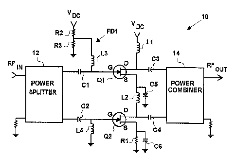
Referring now to FIGURE 1, an rf power amplifier 10 includes solid-state
current devices, n-channel gallium arsenide field-effect transistors,
GaAsFETs, or
FETs, Q1 and Q2 that are connected in series between a positive supply voltage
Vp~ and a ground.
More particularly, a first rf choke L1 connects the supply voltage Vp~ to a
drain terminal of the FET Q1, a second rf choke L2 connects a source terminal
of
the FET Q1 to a drain terminal of the FET Q2, and a resistor R1 connects a
source
terminal of the FET Q2 to a ground.
The rf power amplifier 10 also includes an rf power splitter 12 and an rf
power combiner 14. The rf power splitter 12 is connected to gate terminals of
the
FETs Q1 and Q2, respectively, by coupling capacitors C1 and C2. The rf power
combiner 14 is connected to drain terminals of the FETs Q1 and Q2,
respectively,
by coupling capacitors C3 and C4. And source terminals of the FETs Q1 and Q2
are connected to an electrical ground by decoupling capacitors C5 and C6,
respectively.
A fixed voltage divider FD1, that includes resistors R2 and R3, is
connected to the supply voltage Vp~, and supplies a bias voltage to the gate
terminal of the FET Q1 through a third rf choke L3. The resistor R1 supplies a
negative gate-to-source bias for the gate terminal of the FET Q2 through a
fourth rf
choke L4.
The resistor R1, in setting the gate-to-source bias for the FET Q2, controls
current flow through both FETs, Q1 and Q2. It is important to remember this
fact,
since other embodiments of the present invention use various means for
controlling the gate-to-source bias for the FET Q2, thereby providing means
for
controlling power amplification of the rf power amplifier 10.
Continuing to refer to FIGURE 1, if the supply voltage is 22.0 volts dc, and
if the resistor R1 provides a 2.0 voltage drop between the source terminal of
the
FET Q2 and a ground, assuming equal current through the FETs, Q1 and Q2, the
remaining 20.0 volts will be equally divided, thereby providing 10.0 volts for
each
FET, Q1 and Q2, with the FET Q2 having 22.0 volts applied to the drain and
12.0
volts applied to the source terminal.
CA 02374794 2004-12-30
70828-27
If then, resistances of the resistors R2 and R3 are proportioned to provide
10.0 volts to the gate terminal of the FET Q1, a negative gate-to-source bias
of 2.0
volts will be provided for the FET Q1. In like manner, with 12.0 volts being
applied to the drain terminal of the FET Q2 and 2.0 volts being applied to the
5 source terminal, an electrical ground will be 2.0 volts below the voltage
that is
applied to the source terminal, thereby providing a negative gate-to-source
bias of
2.0 volts for the FET Q2, since the gate terminal of the FET Q2 is connected
to an
electrical ground through the rf choke L4.
In operation, an input signal at an rf input RF,N is split in the rf power
10 splitter 12, amplified in the FETs Q1 and Q2, and combined in the rf power
combiner 14 to provide a power amplified output at an rf output RFour
The amplification function of the FETs Q1 and Q2 is maintained by using
rf chokes, L1, L2, L3, and L4, to keep the rf signal from coupling onto the do
bias
lines and to prevent rf interference between FETs Q1 and Q2; and decoupling
capacitors, C5 and C6, are used to keep the source terminals of both FETs, Q1
and
Q2, at an rf ground.
Since the performance of the rf power amplifier 10 rests heavily on correct
design and application of the rf chokes, L1, L2, L3, and L4, and the
decoupling
capacitors, C5 and C6, their design and selection will be considered in
greater
detail after considering various other embodiments of the present invention.
Referring now to FIGURE 1A, the voltage divider FD1, that includes the
resistors R2 and R3, has been replaced by a variable voltage divider, or
potentiometer, VD1. And an operational amplifier, OP1, configured as a buffer,
has been inserted in series with the rf choke L3. Preferably, the
potentiometer
VD1 and the operational amplifier OP1 are used in all of the embodiments of
the
present invention.
Referring now to FIGURES 1 and 1A, with regard to the potentiometer
VD1 of FIGURE 1A, if any drain-to-source bias imbalances occur between the
FETs, Q1 and Q2, when applying an rf signal, the drain-to-source biases of the
FETs Q1 and Q2 may be equalized by adjusting a wiper 122 of the potentiometer
VD1, thereby adjusting the gate-to-source bias of both FETs, Q1 and Q2.
Continuing to refer to FIGURES 1 and 1A, with regard to the operational
amplifier OP1, the gate current of the FET Q1 must be accounted for when
biasing
CA 02374794 2002-03-06
11
the gate, particularly in high-power rf applications. If the gate current
changes
when the amplifier is tuned across a frequency band or operated over varying
environmental conditions, the operational amplifier OP1 may be inserted
between
the voltage divider and the gate of the FET Q1, as shown, to prevent the
varying
gate current from affecting the fixed voltage divider FD1 and therefore the
bias of
both FETs, Q1 and Q2. A buffer is required since the gate current may be bi-
directional under the varying operating conditions.
Referring now to FIGURE 2, an rf power amplifier, or variable rf power
amplifier, 20 includes like-named and like-numbered components as those in
FIGURE 1, except that an npn bipolar transistor Q3 has been placed in series
with
the FETs Q1 and Q2, and the resistor R1 has been replaced by a resistor R4.
Further, although deleted from FIGURE 2 and all subsequent FIGURES for
the purpose of saving drawing space, the power amplifier 20 and all of the
power
amplifiers that will be described subsequently include: the rf choke L1, the
rf
choke L3, either the voltage divider FD1 of FIGURE 1 or the voltage divider
VD1
of FIGURE 1A, and optionally, the operational amplifier OP1 of FIGURE 1A.
Continuing to refer to FIGURE 2, the npn bipolar transistor Q3 has been
placed in the stack, in totem-pole arrangement, with the FETs Q1 and Q2, with
a
collector terminal of the npn bipolar transistor Q3 connected to the source
terminal of the FET Q2, and with an emitter terminal of the transistor Q3
connected to the resistor R4. Thus, the npn bipolar transistor Q3 dividingly
shares
the supply voltage with the FETs Q1 and Q2, and thereby uses the same current,
even as the FETs Q1 and Q2 of FIGURE 1 dividingly share the supply voltage and
use the same current.
Since GaAsFETs may be biased for linear amplification (Class A
Amplifiers), or semilinear amplification, (Class B or A/B Amplifiers),
amplification is
approximately a linear function of the drain current. Therefore, by placing a
variable current device, such as the transistor Q3, in series with the FET Q2,
the rf
power amplifier 10 of FIGURE 1 becomes the variable rf power amplifier 20 of
FIGURE 2. Power amplification is variably controlled by controlling a voltage
V~AR
to a base terminal of the npn bipolar transistor Q3.
Referring now to FIGURE 3, an rf power amplifier 30 includes like-named
and like-numbered parts as those of the rf power amplifier 20 of FIGURE 2,
except
CA 02374794 2002-03-06
12
that an output power detector 32 and a conditioner 34 are used to feedback a
signal from the rf output RFouT to control the base terminal of the npn
bipolar
transistor Q3, thereby flattening the rf output RFouT with respect to
frequency,
voltage, temperature, and time.
Referring now to FIGURE 4, an rf power amplifier 40 includes like-named
and like-numbered parts as those of the rf power amplifier 20 of FIGURE 2,
except
that a solid-state current device, GaAsFET, or FET, Q4 replaces the npn
bipolar
transistor Q3. As shown, the FET Q4 is in totem-pole arrangement with the FETs
Q1 and Q2, so that the FETs Q1, Q2, and Q4 share the supply voltage. The FET
Q4 is connected as a driver for the FETs Q1 and Q2.
A drain terminal of the FET Q4 is connected to the source terminal of the
FET Q2 by a fifth rf choke L5, the source terminal of the FET Q4 is connected
to
an electrical ground through a resistor R5, a gate terminal of the FET Q4 is
connected to an electrical ground through a sixth rf choke L6, and an rf input
RF,NZ, is connected to the gate terminal of the FET Q4 by a coupling capacitor
C7.
Finally, a decoupling capacitor C8 is connected between the source terminal
and
an electrical ground.
Since the rf power amplifier 40 includes three FETs, Q1, Q2, and Q4, that
are stacked in a totem-pole arrangement, they all share the supply voltage,
even
though the FET Q4 is configured as a driver for the FETs Q1 and Q2.
Since the FETs Q1 and Q2 each use about 10.0 volts of the total supply
voltage, the voltage remaining for use with other field-effect devices in the
stack,
such as the FET Q4, is limited. Therefore, the FET Q4 is self-biased to a
quiescent
point close to saturation (Idss) to result in a lower drain-to-source bias.
Further, as
stated above, the bias voltage on the gate of the FET that is on the bottom of
the
stack sets the current for all FETs in the stack. To avoid increased current
draw, a
lower power GaAsFET, for the FET Q4, is used so that when biased close to
saturation the current through the stack is correct for FETs Q1 and Q2.
Continuing to refer to FIGURE 4, if a GaAsFET of even lower power is
used for the FET Q4 so that the current flow through the FETs Q1 and Q2 is
insufficient, a resistor R6 may be connected in parallel with the FET Q4 that
is
used as the driver. As shown in FIGURE 4, interconnecting a pair of jumper
terminals 42 will place the resistor R6 in parallel with the FET Q4, thereby
sharing
CA 02374794 2002-03-06
13
the current flow with the FET Q4, and thereby avoiding damage to the FET Q4 if
its current capacity is insufficient.
The driver, FET Q4, is self-biased and its output is split by the rf power
splitter 12 to drive the two final stage power FETs Q1 and Q2, but the FET Q2
requires a negative gate-to-source bias, even as described previously for the
FET
Q1. The negative gate-to-source bias for the FET Q2 is provided in the same
manner as described for the FET Q1. That is, a voltage divider FD2 includes
resistors R7 and R8. The negative gate-to-source bias for the FET Q2 is
supplied
through a seventh rf choke L7. Optionally, the voltage divider FD2 may be
replaced by a duplication of the circuit of FIGURE 1A, including the
operational
amplifier OP1 for gate current management.
In operation, the rf input RF,NZ, that is delivered to the FET Q4 through the
capacitor C7, is amplified in the FET Q4, is delivered to the rf input RF,N of
the rf
power splitter 12 through a capacitor C9, and is power amplified by the FETs
Q1
and Q2.
Referring now to FIGURE 5, an rf power amplifier, or variable rf power
amplifier 50 includes like-named and like-numbered parts as those of FIGURE 4,
except that the npn bipolar transistor Q3 is added to the totem-pole
arrangement
on the bottom of the stack, thereby dividingly sharing the supply voltage, and
thereby adding variable amplification of power to the rf power amplifier 40 of
FIGURE 4.
Referring now to FIGURE 6, an rf power amplifier, or variable rf power
amplifier 60 includes like-named and like-numbered parts as those of FIGURE 5,
except that the npn bipolar transistor Q3, is placed in parallel with the
driver FET
2 5 Q4.
Therefore, in the rf power amplifier 60, constant current flow through the
FETs Q1 and Q2, as controlled by the FET Q4 is supplemented by variable
control
of current flow by selectively controlling voltage applied to the base
terminal of
the npn bipolar transistor Q3, thereby providing a variable rf power
amplifier.
Referring now to FIGURE 7, an rf power amplifier 70 includes like-named,
like-numbered, and like-functioning parts as those of FIGURE 5, except that
the
power detector 32 and the conditioner 34 of FIGURE 3 are used to flatten the
output power of the rf power amplifier 70, as described in conjunction with
CA 02374794 2002-03-06
14
FIGURE 3. Otherwise, operation of the rf power amplifier 70 is the same as
described for the rf power amplifier 50 of FIGURE 5.
Referring now to FIGURE 8, an rf power amplifier 80 includes like-named,
like-numbered, and like-functioning parts as those of FIGURE 6, except that
the
power detector 32 and the conditioner 34 of FIGURE 3 are used to flatten the
output power of the rf power amplifier 80, as described in conjunction with
FIGURE 3. Otherwise, operation of the rf power amplifier 80 is the same as
described for the rf power amplifier 60 of FIGURE 6.
Referring now to FIGURE 9, an rf power amplifier 90 includes like-named,
like-numbered, and like-functioning parts as those of FIGURE 1, except that
the rf
power combiner 14 has been omitted, so that two rf outputs, RF1 ouT and
RF2ouT,
are provided.
By not recombining the rf outputs, RF1 our and RF2ouT of FETs Q1 and Q2,
the amplifier may be used as a dual output amplifier/transmitter. The dual rf
outputs, RF1 ouT and RF2ouT may be used for driving multiple antennas, not
shown,
not an inventive part of the present invention.
Referring now to FIGURE 10, an rf power amplifier 100 includes like-
named, like-numbered, and like-functioning parts as those of FIGURE 9, except
that variable phase shifters, VPS1 and VPS2, are interposed between the FETs,
Q1
and Q2, and the rf outputs, RF1 ouT and RF2ouT. Optionally, only one phase
shifter, VPS1 or VPS2, may be used. The rf power amplifier 100 may be used for
driving phased antenna arrays.
Referring now to FIGURE 11, an rf power amplifier 110 includes like-
named, like-numbered, and like-functioning parts as those of FIGURE 10; except
that two output power detectors, 32 and 112, a conditioner 114, the transistor
Q3,
and a summing resistor R9 are added.
As shown in FIGURE 11, the conditioner 114 has two inputs, 116A and
116B, that are connected to the power detectors, 32 and 112, respectively, and
two outputs, 1 18A and 1 18B. The output 118A is connected to the base
terminal
of the transistor Q3, and functions with the transistor Q3 as described in
conjunction with FIGURE 3. The output 118B of the conditioner 114 is connected
to a summing node 120 of the voltage divider FD1 by the resistor R9.
CA 02374794 2004-12-30
70828-27
In addition to flattening the rf outputs, RFIo~T and RF2ouT as a function of
the connection of the output 118A of the conditioner 114 to the transistor Q3,
the
output 1188 of the conditioner 114 automatically equalizes the dual rf
outputs,
RF1 ouT and RF2ouT.
5 That is, as mentioned previously, the rf outputs of the FETs Q1 and Q2
may be balanced by adjusting the voltage divider VD1 of FIGURE 1A. In like
manner, the rf outputs, RF1 ouT and RF2ouT, of the FETs Q1 and Q2 are ,
automatically balanced by the power detector 112 and the output 1188 of the
conditioner 114. Feedback from the output 1188 variably adjusts the gate-to-
10 source bias of the FET Q1 by summing, at the summing node 120, the output
1188
of the conditioner 114 with that of the voltage divider FD1.
Referring now to FIGURE 11A, if the potentiometer VD1 of FIGURE 1A is
used instead of the voltage divider FD1, the summing resistor R9 is connected
to
the wiper 122 of the potentiometer VD1 at the node 120. As discussed with
15 FIGURE 1A, and as shown in FIGURE 11A, the operational amplifier OP1 is
used
as a buffer.
Referring now to FIGURE 12, an rf power amplifier 130 includes like-
named and like-numbered parts as those in the rf power amplifier 10 of FIGURE
1,
except as specified. More particularly, the rf power amplifier 130 includes a
three-
way power splitter 132, a three-way power combiner 134 that is optional, a
solid-
state current device, gallium arsenide FET, GaAsFET, or FET, Q5, a decoupling
capacitor C10, an rf choke L8, coupling capacitors C11 and C12, an rf choke
L9,
and the voltage divider FD2.
If the voltage of the voltage source permits, additional FETs or bipolar
transistors may be included in the stack as taught in conjunction with
previous
drawings, or as will be taught subsequently, thereby saving the current that
the
additional FETs and/or bipolar transistors would draw. Further, current
control or
feedback may be added as shown and described previously, or as shall be
described subsequently.
As shown in FIGURE 12, the rf power amplifier 130 optionally includes
the three-way combiner 134. Thus, variations of the rf power amplifier 130
include omitting the three-way combiner 134, thereby producing three rf
outputs,
as indicated by arrows in dash lines, any or all of which may be variably
shifted as
shown in FIGURE 10.
CA 02374794 2004-12-30
70828-27
16
Referring now to FIGURE 13, an rf power amplifier 140 includes like-
named and like-numbered components as those shown in FIGURE 6, except that a
voltage controlled oscillator, or VCO,,142 replaces the FET Q4, and a pair of
jumper terminals 144 and a pair of jumper terminals 146 are added. The VCO
142 includes a varactor VC1, an inductor L10, a capacitor C13, the rf choke
L6, a
solid-state current device, gallium arsenide FET, GaAsFET, or FET Q6, and the
resistor R5. The VCO 142 produces an rf output signal that is varied i~
frequency
by changing a control voltage V~ applied to the varactor VC1.
As shown in FIGURE 13, the VCO 142 drives the rf input RF,N of the
power splitter 12. However, if the VCO 142 does not provide sufficient rf
power
for the power splitter 12, a decoupling capacitor C16 may be added by
interconnecting the pair of jumper terminals 144.
If the current drain of the FET Q6 is less than desired for the FETs Q1 and
Q2, the resistor R6 may be added by interconnecting the jumper terminals 42;
and/or the current flow may be variably increased by interconnecting the pair
of
jumper terminals 146, thereby placing the transistor Q3 in parallel with the
FET
Q6.
Using a FET with the VCO 142, such as the FET Q4, and placing the FET
Q6 in the stack, eliminates the additional current drain of the FET Q6.
Alternately,
the VCO may be used to drive a bipolar transistor, such as the transistor Q3.
By
placing the transistor Q3 in the stack, in the place of the FET Q6, similar
advantages are achieved.
Referring now to FIGURE 14, an rf power amplifier 150 includes like-
named and like-numbered components as in FIGURE 13, except for the addition of
the FET Q4, a fixed voltage divider FD3 that includes resistors R10 and R11,
an rf
choke L11, a resistor R12, a pair of jumper terminals 152, an rf choke L12, a
decoupling capacitor C14, and a coupling capacitor C15.
The rf power amplifier 150 functions as described for the rf power
amplifier 140 of FIGURE 13, except for insertion of the FET Q4 as a driver.
The
jumper terminals 152 and the resistor R12 provide means for adding current
flow
to that of the FET Q4, as described previously, and the resistor R6 provide
means
for adding current flow to the FET Q6, thereby increasing current flow through
the
FETs Q1 and Q2.
CA 02374794 2004-12-30
70828-27
17
Referring now to FIGURE 15, an rf power amplifier 160 includes like-
named and like-numbered components as in FIGURE 14, except the FETs Q4 and
Q6 are connected in parallel, instead of being connected in series as in
FIGURE
14. In addition, a connection between the source terminal of the FET Q2 and
drain terminals of the FETS Q4 and Q6 includes rf chokes L13 and L14. An rf
choke L15 is connected from the gate of the FET Q4 to an electrical ground,
and
resistors R13 and R15 are added.
By placing the FETs Q4 and Q6 in parallel, these two FETs share the
current flow through the FETs Q1 and Q2, thereby reducing the need to shunt
additional current flow past the FETs Q4 and Q6 by the use of a parallel-
connected
resistor, resistor R13. That is, the combined current flow through the FETs Q4
and
Q6, for some applications, may still be lower than the current flow that is
desired
for the FETs Q1 and Q2, but the need for current shunting will be less for the
FIGURE 15 embodiment than it is when the FETs Q4 and Q6 are connected in
series, as in FIGURE 14.
Referring now to FIGURE 16, an rf power amplifier 170 is provided for
relatively-low power applications. The rf power amplifier 170 includes like-
named
and like-numbered components as those shown and described in conjunction with
FIGURE 13, except for omission of the FET Q2, the power splitter 12, and the
power combiner 14, and except for the addition of an npn bipolar transistor
Q7, a
pair of jumper terminals 172, and a resistor R16.
As described in conjunction with FIGURE 13, the VCO 142 includes the
FET Q6, but in the embodiment of FIGURE 16, the FET Q1 is the sole and final
source of amplifier rf power, since the FET Q2 and the power splitter 12 have
been
omitted.
In like manner as shown and described in conjunction with FIGURE 13,
the bipolar transistor Q3 and/or the resistor R6 may be used to shunt the
current
flow through the FET Q6, thereby providing a more adequate flow of current
through the FET Q1 that supplies rf power.
That is, connection of the jumper terminals 42 provides an increase in rf
power, connection of the jumper terminals 146 provides variably-increased
power,
and connection of both pairs of jumper terminals, 42 and 146, provides rf
power
that is both increased and variably increased. Finally, as previously
discussed, the
CA 02374794 2002-03-06
18
capacitor C8 may be used to increase the power output of the VCO 142 by
connecting jumper terminals 172.
The rf power amplifier 170 may be used as a stand-alone
amplifier/transmitter for applications in which relatively lower rf power is
sufficient.
Alternately, the rf power amplifier 170 may be used, in parallel with a stack
of
FETs, such as the FETs Q1, Q2, and Q5 of FIGURE 12.
Referring now to FIGURE 17, an rf power amplifier 180 includes like-
numbered and like-named components as those in the rf power amplifier 10 of
FIGURE 1, except for omission of the power splitter 12, and addition of a
resistor
R17.
Two rf inputs, RF1,N and RF2,N, are connected to the FETs Q1 and Q2,
respectively. The two rf inputs, RF1,N and RF2,N, may be of different
frequencies
within the range of the power combiner 14, may be of different rf levels, and
may
be modulated by different types of modulation. Further, gains of the FETs Q1
and
Q2 may be set differently, by any suitable means, such as selectively
determining
drain-source voltages.
The rf power amplifier 180 has the unique ability to produce a single rf
output that includes the two separately amplified rf outputs, although power,
equal
to the rf output, RFouT, is dissipated across the resistor R17. The rf output,
RFour~
is equal to (A,RF1,N/2) + (A2RF2""/2), where A, and AZ are gains of the FETs
Q1
and Q2, respectively.
Referring now to the rf power amplifiers of FIGURES 1-16, the objective of
all of the totem-pole FET amplifiers shown and described herein is to minimize
power loss in a voltage regulator circuit, thereby increasing the power
efficiency of
the rf amplifier. The only limitation to the number of devices that can be
stacked
is the maximum voltage that is available.
It should be understood that the rf power amplifiers shown and described
herein can be modified to include features and components shown and described
in conjunction with other embodiments.
For instance, the rf power amplifiers shown and described herein may
include such features as dual or triple rf outputs, phase-shifted rf outputs,
variable
control of power, current shunting, rf feedback, buffer control of gate-source
CA 02374794 2004-12-30
70828-27
19
voltages by an operational amplifier configured as a buffer, and use of a VCO
to
generate an rf input.
Referring now to FIGURES 1-11 and 13-15, the rf power splitter 12 and
the rf power combiner 14 are typically quadrature hybrids or Wilkinson power
dividers. However, any practical method of splitting and combining may be used
to practice the present invention.
The three-way splitter 132 and the three-way combiner 134 may be
constructed in accordance with textbook technology. For instance, technical
information for constructing splitters that will split three or more ways can
be
found in Microwave Engineering, Second Edition, by David M. Pozar, pages 363-
368, New York: John Wiley & Sons, Inc., 1998.
Referring again to FIGURE 1, as stated previously, the amplification
function of the FETs, such as the FETs Q1 and Q2, is maintained by using rf
chokes, such as the rf chokes, L1, L2,, L3, and L4, to keep the rf signal from
getting
onto the do bias lines and to prevent rf interference between the series-
connected
FETs; and decoupling capacitors, such as the capacitors C5 and C6, are used to
keep the sources of FETs at an rf ground.
The selection of the decoupling capacitors and chokes are both critical to
the rf performance of the circuit, particularly for high-power rf amplifiers,
although
selection of decoupling capacitors is the most critical. Decoupling
capacitors, such
as the decoupling capacitors CS, C6, C8, C10, C14, and C16 are selected for
both
resonant frequencies at or very near to the circuit-operating frequency and
the
lowest possible effective (or equivalent) series resistances (ESRs). The rf
chokes,
such as the rf chokes L1, L2, L3, and L4, preferably are inductors with self
resonant
frequencies at or very near to the circuit-operating frequency.
Referring now to FIGURE 18, the microwave circuit model of an inductor
is a series resistor Rs and an inductor .L in parallel with a capacitor C. The
resistor
Rs represents the do coil resistance along with the increased wire resistance
at rf
frequencies due to the skin effect (the effect of the current being
concentrated
nearer to the surface of the wire) as the operational frequency is increased.
The
capacitor C represents the distributed capacitance between the parallel
windings of
the coils. Inductance of the inductor L is the nominal component inductance.
CA 02374794 2004-12-30
70828-27
At operation below the self resonant frequency, the impedance of an
inductor increases as frequency increases. At the inductor self resonant
frequency,
the inductor, as represented by the parallel VC circuit of FIGURE 18,
resonates as
an open circuit creating a maximum impedance to the rf signal. At operation
5 higher than the self resonant frequency, the distributed capacitance C
dominates
the rf impedance resulting in the impedance decreasing with increasing
frequency.
The inductor self resonant frequency equation is given as: FSR a
1/[2rr'''~(LC)).
The resistance Rs limits the maximum impedance of the self resonant
inductor. That is, the quality factor (Q) of the inductor is the ratio of an
inductor's
10 reactance to its series resistance Rs. High-Q inductors, with very low
resistances
Rs, have very high self resonant impedances, but for only~a narrow bandwidth.
Lower-Q inductors, with higher resistances Rs, have lower self resonant
impedances for a much broader bandwidth.
This self resonant feature is used in the circuit to prevent the rf signal
from
15 coupling onto the do bias lines and to aid the decoupling capacitors in
preventing
rf crosstalk between the two, or more, FETs. For narrow-band operation, very
high-
Q inductors are desired to maximize series impedance. Quarter wave
transformers
may also be used for this function in narrow-band applications. For broad-band
operation, lower-Q inductors are desired to obtain a high impedance across a
20 larger bandwidth. In either application, the inductor must be capable of
passing
the maximum do current without breakdown.
Utilizing the self resonant characteristics of decoupling capacitors, such as
the capacitors C5 and C6, is required to optimize rf performance while
maximizing
dc-rf conversion efficiency, particularly in applications where the rf power
exceeds
100 milliwatts.
Referring now to FIGURE 19, the microwave circuit model of a capacitor
is an inductor L in series with a resistor Rs in series with a capacitor C.
The
inductor L represents the inductance of the leads and the capacitor plates.
The
resistor Rs represents the equivalent series resistance, or ESR, of the
capacitor.
Capacitor dielectric losses, metal plate losses, and skin effects all
contribute to the
ESR. The capacitor C is the nominal component capacitance.
These parasitic effects of a capacitor at microwave frequencies alter its
impedance characteristics in the opposite manner as that of an inductor. At
CA 02374794 2004-12-30
70828-27
21
operation below the self resonant frequency, a capacitor decreases in
impedance as
frequency increases. At the capacitor self resonant frequency, a capacitor; as
represented by the series UC circuit of FIGURE 19, resonates as a short
circuit
creating a minimum impedance to the rf signal. At frequencies higher than the
self resonant frequency, the lead and plate inductance dominates the rf
impedance
resulting in the impedance increasing with increasing frequency. The capacitor
self resonant frequency equation is: FsR = 1/[2rr'''d(LC)), which is the same
as for
the inductor.
The rf impedance of a capacitor at self resonant frequency is equal to the
ESR. As in the case of the inductor, the quality factor Q of a capacitor is
the ratio
of a capacitor's reactance to its ESR, or alternatively the quality factor Q
is 1/DF
where DF is the dissipation factor of the capacitor. High-Q capacitors, with
very
low ESR, have very low self resonant impedances, but for only a narrow
bandwidth. Lower-Q capacitors, with higher ESR, have lower self resonant
impedances for a much broader bandwidth. Presently, the preferred capacitor
dielectric to minimize capacitor ESR is porcelain. Porcelain has a dissipation
factor, DF, of 0.00007, the lowest of afl currently available capacitor
dieiectrics.
To minimize the rf impedance from the FET source terminal to a circuit
ground, decoupling capacitors with self resonant frequencies at or very near
to the
amplifier operational frequency are required in high-power rf applications.
The power dissipated in the decoupling capacitor is Pp,ss = Iz*ESR, where
1 is the root-mean-square, or rms, of the rf current through the capacitor.
Alternatively, Pp,ss = PRF*ESR/Z where Z is the circuit load impedance,
typically 50
ohms, and PRF is the rf output power of the FET.
For optimal performance, the'ratio of FET rf output power, PRF, to
decoupling capacitor power dissipated, Pp,ss, should be no less than 2000 for
medium rf power, which is defined as 100 milliwatts to 2.0 Watts FET rf output
power. For high-power rf applications, which is defined as FET output power
greater than 2.0 Watts, the PR~/Pp,ss ratio should be no less than 5000.
Very high-Q decoupling capacitors are necessary to minimize series
impedance to a circuit ground, whether it be for narrow-band, or wide-band
operation. For broad-band operation, multiple high-Q decoupling capacitors
with
CA 02374794 2004-12-30
70828-27
22
self resonant frequencies selected at several points in the operating-
frequency band
are optimally selected for minimum ESR across a broad-frequency band.
Referring now to FIGURE 20, two or more multiple porcelain dielectric
capacitors Ca-n, each with self resonant frequencies at or near the amplifier
operational frequency, are connected in parallel from the FET source terminal
to a
circuit ground to achieve the low required decoupling capacitor ESR for high-
power rf applications.
Paralleling a plurality of capacitors at the self resonant frequency divides
the ESR in the same manner as paralleling resistors. However, if a capacitor
is not
available with a resonant frequency that closely matches an operating
frequency for
narrow-band operation, two paralleled capacitors are chosen with one having a
resonant frequency above the narrow-band frequency, and the other having a
resonant frequency below the narrow-band frequency.
Referring now to FIGURES 1-17 and 20, preferably the effective series
resistances of the decoupling capacitors C5, C6, C8, C10, C14, and/or C16 each
have an effective series resistance of less than 0.4 ohms divided by the rf
output
power. More preferably, all of these decoupling capacitors have an effective
series
resistance of 0.20 ohms divided by the rf output power.
If the required ESR, as calculated by either of the formulas given above, for
any or all of the decoupling capacitors C5, C6, C8, C10, C14, and C16 cannot
be
met by a single capacitor, any or all may be replaced by any number of the
paralleled capacitors Ca-n, as shown in FIGURE 20.
Porcelain capacitors presently have the lowest dielectric resistance and are
preferred for minimizing the effective rf impedance. Porcelain capacitors,
model
6005, manufactured by American Technical Ceramics of Huntington Station, New
York, are suitable for rf decoupling as taught herein.
Model 6005 capacitors that are available from American Technical
Ceramics, their self resonant frequencies, their capacities, and their
effective series
resistances, are included in the following table.
CA 02374794 2004-12-30
70828-27
23
Table 1: Porcelain Capacitors
Self Resonant Frequencies vs. ESRs
Self resonant Freq. Capacitance ESR
1 GHz 100 pF 0.07 ohms
2 GHz 40 pF 0.09 ohms
4 GHz 15 pF 0.15 ohms
8 GHz 3 pF 0.20 ohms
16 GHz 1 pF 0.30 ohms
Referring now to FIGURE 20 and Table 1, as an example of capacitor
paralleling to achieve a required ESR, assume an rf output of 5.0 Watts, using
the
0.2 ohms/Watts criteria, the ESR of the decoupling capacitor should be 0.04
ohms.
Assuming an operating frequency of 4 GHz, from Table 1, the ESR for a
porcelain
capacitor is 0.15 ohms, so four capacitors must be paralleled to achieve the
req a i red ES R.
Packaged GaAsFETs typically have a considerable source lead parasitic
inductance. By choosing a decoupling capacitor, or capacitors, with a value
that
resonates with the source lead inductance, the true FET source impedance to a
circuit ground is further reduced.
Therefore, the package, or lead, inductance of the capacitor, or capacitors,
should be considered in the equation for resonance when selecting a capacitor
to
resonate with the GaAsFET source lead inductance. Additionally, several
parallel
capacitors with a combined reactance that resonates with the GaAsFET source
lead
inductance are selected to minimize the decoupling capacitor ESR and maximize
efficiency in high-power rf applications (FET rf output in excess of 2.0
Watts).
Often in high-power packaged FETs the source terminal is the body of the
device and is connected to.a mounting flange. Conventionally, the flange is
connected directly to a circuit ground with metallic screws to achieve minimal
rf
impedance to an electrical ground and to maximize thermal conductivity between
the FET and a circuit ground, which is most often a chassis serving as a heat
sink
to the FET. However, in the present invention, the source terminals of the
FETs are
electrically isolated from a circuit ground.
Referring now to FIGURE 21, a thermally conductive, electrically
insulating pad 190 is inserted between a FET mounting flange 192 of a FET 194
and a heat sink, or chassis, 196 to allow the dissipated heat of the FET 194
to flow
CA 02374794 2004-12-30
70828-27
24
from the FET 194 to the heat sink 196 while maintaining electrical isolation.
The
electrical insulating material of the pad 190 should have no higher than
0.5° C/Watt thermal resistance. An irisulating material with a higher
thermal
resistance, combined with the thermal resistance of the FET 194 and the
ambient
temperature, may result in the internal junction temperature of the FET 194
being
excessive, thereby causing reduced reliability or destruction of the FET 194.
A suitable material for the insulating pad 190 is DeItaPad Thermally
Conductive Insulator, Part Number 174-9 Series, manufactured by Wakefield
Engineering of Pelham, NH. The material for the insulating pad 190 is 0.22
millimeters (0.009 inches) thick, has a thermal resistance of 0.25°
C/W, a resistivity
of 10'3 megohms per cubic centimeter of volume, and a 5000 volt breakdown.
The mounting flange 192 is held in heat-conducting contact with the
insulating pad 190 and with the heat sink 196, with non-ferrous, or non-
conductive, screws 198. The tensile strength and stretching of the screw
material
along with the manufacturer-recommended FET mounting torque must be taken
into account when selecting fasteners.
Although the preceding discussion has focused on use of GaAsFETs in
totem-pole circuit at microwave frequencies for frequencies of 3 GHz, or
higher,
there are also efficiency advantages to using the totem-pole circuit at lower
frequencies, such as the "L" and "S" bands (1 to 3 GHz).
At these lower frequencies, silicon bipolar transistors operated in Class C
are the most commonly used amplification device. However, GaAsFETs, in totem-
pole arrangement, provide an improvement in amplifier efficiency over that
achieved by the use of silicon bipolar transistor amplifiers.
There are two basic reasons for this improvement in efficiency. First, the
GaAsFETs, with efficiencies up to seventy percent, are inherently more
efficient
than silicon bipolar transistors at "L" and "S" bands. Second, the high gain
of
GaAsFETs at "L" and "S" bands (up to 20 Db) versus silicon bipolar transistors
(about 10 Db) result in fewer total amplification stages to achieve the
desired rf
power output.
Therefore, the use of GaAsFETs at these lower frequencies results in the
elimination of stages) and allows for lower power driver stages. And the high
gain
of the GaAsFETs makes the power-added efficiency (PAE) higher than that of
CA 02374794 2004-12-30
70828-27
traditional Class C silicon bipolar transistors despite the Class A or A/B
operation of
the GaAsFET.
While GaAsFETs have been shown and described, it should be understood
that the principles taught herein may be applied to other types of solid-state
current
5 devices.
In summary, the present invention can be characterized as providing rf
power amplifiers, both constant and variable power, in which at least~two
solid-
state current devices, which preferably are gallium arsenide field-effect
transistors
(GaAsFETs), dividingly share the supply voltage, and share the same current.
10 Thus, the amplifiers of the present invention can be characterized as
permitting use of linear regulators with significantly less voltage drop over
the pass
element, thereby providing distinct advantages over the prior art practice of
using
either a linear regulator with a high voltage drop over the pass element, or
alternately, a switching regulator.
15 Further, the present invention provides rf power amplifiers, both fixed and
variable, in which a single rf output is produced, in which two or more rf
outputs
are produced, or in which two or more rf outputs may be variably phase
sfiifted.
More succinctly, the present invention can be characterized as connecting
a plurality of field-effect devices in series for do operation while the same
devices
20 operate in parallel for rf operation. Additionally, the present invention
provides a
method for minimizing the rf impedance from a field-effect device source to a
circuit ground, thereby maximizing dc-rf conversion efficiency while
minimizing
interference between field-effect devices, and between field-effect devices
and
power supply, by design and selection of decoupling capacitors and rf chokes.
25 While specific apparatus and method have been disclosed in the preceding
description, it should be understood that these specifics have been given for
the
purpose of disclosing the principles of the present invention, and that many
variations thereof will become apparent to those who are versed in the art.
Therefore, the scope of the present invention is to be determined by claims
included herein without any limitation by numbers that may be parenthetically
inserted in the claims.
CA 02374794 2002-03-06
26
Industrial Applicability
The present invention is applicable to rf amplifiers, and particularly to rf
amplifiers that use gallium arsenide FETs in airborne applications wherein the
supply voltage exceeds the working voltage for gallium arsenide FETs.