Note : Les descriptions sont présentées dans la langue officielle dans laquelle elles ont été soumises.
CA 02375563 2001-12-21
WO 00/79313 PCT/US00/40253
- 1 -
TITLE OF THE INVENTION
NUMERICAL APERATURE INCREASING LENS (NAIL) TECHNIQUES
FOR HIGH-RESOLUTION SUB-SURFACE IMAGING
S
CROSS REFERENCE TO RELATED APPLICATIONS
This application claims priority under 35
U.S.C. ~119(e) to Provisional Application
No. 60/140,138, filed June 21, 1999; the disclosure of
which is incorporated herein by reference.
ACKNOWLEDGMENT OF GOVERNMENT SUPPORT
This invention was made with government support
under Grant Number ECS-9625236 awarded by the National
Science Foundation and under Contract Number 1210800
awarded by DARPA. The Government has certain rights in
the invention.
BACKGROUND OF THE INVENTION
Standard optical microscopy is not capable of
obtaining a transverse resolution with a definition
better than approximately half a wavelength of light due
to the diffraction limit, also termed the Rayleigh or
Abbe limit. The diffraction limited spatial resolution
is ~,/(2 NA) where 7~ is the wavelength of collected light
in free space. The Numerical Aperture is defined as NA
- n sinBa where n is the refractive index of the
material and 9a is the collection angle, the half-angle
of the optical collection area. In order to improve
resolution of diffraction limited microscopy the NA must
be increased. The highest NA values for standard
CA 02375563 2001-12-21
WO 00/79313 PCT/US00/40253
- 2 -
microscope objectives in air ambient are less than 1,
with typical best values around 0.6.
One method to increase the NA is to increase the
index n of the material where the collection focus is
formed. Insertion of a high index fluid, such as oil,
between the microscope objective lens and the sample
allows for higher NA, with typical best values around
1.3. Similarly, a microscope design utilizing a high
index hemispherical lens, called a Solid Immersion Lens
(SIL), closely spaced to the sample can provide a
resolution improvement of 1/n. The SIL microscope
relies on evanescent coupling between the light focussed
in the high index SIL AND THE SAMPLE. Previous patents
on SIL microscopy describe arrangements where the light
is focussed at the geometrical center of the spherical
surface of the SIL.
Subsurface imaging of planar samples is normally
accomplished by standard microscopy. The NA remains the
same when imaging below the surface of higher index
samples, because the increase in index is exactly
counterbalanced by the reduction of sin6a from
refraction at the planar boundary. Standard subsurface
imaging also imparts spherical aberration to the
collected light from refraction at the same planar
boundary. The amount of spherical aberration increases
monotonically with increasing NA. Subsurface imaging
has been conducted through Silicon substrates at
wavelengths of 1.0 ~m and longer, with best values of
transverse resolution around 1.0 ~,m.
The use of SIL microscopy has been suggested for
subsurface imaging wherein the light phase fronts are
geometrically matched to the SIL surface. However, the
CA 02375563 2001-12-21
WO 00/79313 PCT/LJS00/40253
- 3 -
method described is limited to an arrangement where a
hemispherical lens collects light from a focus at the
geometrical center of the spherical surface of the lens.
In this case, the resolution improvement is limited to
1/n, and the spherical aberration free area is limited
to a point. An image can be formed by scanning the
sample and SIL where the scan precision is relaxed by a
factor of n. An image can also be formed by scanning
the sample and holding the SIL stationary. The
characteristics of the invention described below are an
improvement over those of standard and SIL microscopy
for many sub-surface applications.
BRIEF SUMMARY
The present invention provides a substrate surface
placed lens for viewing or imaging to or from a zone of
focus within the substrate and providing an increase in
the numerical aperture of the optical system over what
it would be without the lens. The enhanced numerical
aperture translates into an improvement in resolution in
collecting or illuminating. The focus at a specific
zone within the substrate is made aberration free,
providing a broad lateral extent to the field of view.
Substrate and lens material are close if not identical
in index of refraction, n.
The invention finds application in viewing
semiconductor devices and circuits; bio/chem specimens
from the underside of an attachment surface, layered
semiconductor and dielectrics such as boundaries of
Silicon-on-Insulator substrates, and read/write
functions of buried optical media.
CA 02375563 2001-12-21
WO 00/79313 PCT/US00/40253
- 4 -
DESCRIPTION OF THE DRAWING
These and other features of the invention are
described below in the Detailed Description and in the
accompanying Drawing of which:
S Fig. 1 illustrates an imaging system having a
numerical aperture increasing lens (NAIL) according to
the invention:
Fig. 2a is a sectional view of a NAIL and substrate
in typical viewing relationship;
Fig. 2b is a sectional view of a NAIL and viewing
objective for viewing into the interior of a substrate;
Fig. 2c is a sectional view of a generalized NAIL
and substrate relationship illustrating a range of
applications for the invention;
Fig. 3 is a sectional view of a medium illustrating
the geometric and mathematical relationships of NAIL
surfaces and planes of aberration free focus;
Figs. 4a- 4b illustrate additional uses for a NAIL
of the invention in inspecting specimens on a bottom
surface of a substrate;
Fig. 5 illustrates the application of the invention
in use in specimen viewing under a cover slip;
Fig. 6 illustrates the use of the invention in the
area of read/write media;
Fig. 7a - 7d illustrate actual images from the use
of the invention in viewing semiconductor structure;
Fig. 8 illustrates the invention in SOI devices for
boundary inspection;
Fig. 9a -9b illustrate the use of the invention in
arrays;
Fig. 10 illustrates a set of NAILS according to the
invention.
CA 02375563 2001-12-21
WO 00/79313 PCT/US00/40253
- 5 -
DETAILED DESCRIPTION
The present invention provides a viewing
enhancement lens (NAIL) which functions to increase the
numerical aperture or light gathering power of viewing
optics such as a microscope used to view structure
within a substrate such as a semiconductor wafer or chip
or of imaging optics used to expose material such as
data media. The result is to increase the resolution of
the system by a factor of between n and n2 where n is
the index of refraction of the lens and substrate.
While the lens and substrate are typically of the same
index of refraction, a near match will provide similar
advantages.
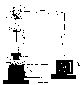
Fig. 1 illustrates such a viewing system in which a
computer controlled XYZ motion support 12 holds a
specimen 14 in a holder 16. A numerical aperture
increasing lens (NAIL) 18 is placed over the specimen.
The NAIL and specimen typically are polished to allow an
intimate contact as free of air space as possible, at
least within a fraction of a wavelength sufficiently
small to avoid reflection effects at the NAIL and
substrate boundary. Light from objects within the
substrate 14, typically from back illumination provided
by holder 16 or from surface illumination from above,
passes through the NAIL 18 and thence through an
objective lens 20 and exit lens 24 of a microscope
system 26 into a video camera 30 or other viewing,
recording or imaging element. Signals from the camera
30 are fed to a computer 32 or other processing, storage
and/or viewing system for display and recordation. This
allows for the recordation of a sequence of images over
CA 02375563 2001-12-21
WO 00/79313 PCT/US00/40253
- 6 -
time, which in turn allows for time-resolved
measurements. The computer may also be programmed to
operate the stage 12 for manual or automated scanning in
X, Y, and/or Z to capture images over a two or three
s dimensional region.
Fig. 2a illustrates a NAIL 18' and substrate 14' in
larger scale. The NAIL 18' typically is less than a
complete hemisphere, having a vertical thickness D, and
thus its center, distant from the outer surface by the
radius of curvature, R, will be located within the
substrate 14' at a point 40. While the NAIL will
increase the numerical aperture of the viewed objects as
noted above, it is also desired to have a view which is
aberration free. There is a spherical surface within
the substrate, depending on its depth, at which focus
occurs and aberration free viewing is obtained. This is
deeper than the point 40 as explained below. There is a
distance either side of this spherical surface at which
the field of view is also aberration or substantially
aberration free, giving a plane region where objects can
be viewed with increased resolution and freedom from
aberrations. With X the distance into the substrate of
the field of view, then D = R(1+1/n)-X. Radiation phase
fronts passing through the NAIL in either direction are
geometrically distinct from the convex surface of the
NAIL thereby providing viewing into or from a substrate
depth well beyond the NAIL.
Fig. 2b shows viewing within a substrate 14"
through a NAIL 18" by an objective 42 of a field of
view 44 at the bottom of the substrate 14" . The field
of view can for example include the underside of
processed regions of a semiconductor wafer containing
CA 02375563 2001-12-21
WO 00/79313 PCT/US00/40253
information relevant to the quality of the resulting
semiconductor chip or other element. In general, as
shown in Fig 2c, the NAIL 18" ' and a substrate 14" '
can be any elements where it is desired to view with
enhanced resolution into a field of view within the
substrate. Examples include microscope slide and cover
glass with a NAIL on top and thermal imaging of heat
emitting semiconductors in operation.
Fig. 3 is of a unitary, solid object 50, an upper
part 52 of which represents the NAIL of the invention
and the remainder a substrate that is to be viewed into
to see a field of view at the spherical surface 54 free
of aberration. An imaginary plane 58 marks the dividing
line between the NAIL and the substrate. The surface 54
is defined by R/n as the depth below the center 60 of
curvature of the NAIL 52.
For optimal resolution, the optics of the
microscope are best matched to those of the NAIL. This
is achieved when the following relation is satisfied:
s = (-fl' )/R(n+1/n);
where fl is the objective focal length, and the
inter lens principle points distance (objective to exit
lens principle points) - s + fl + f2, f2 being the exit
lens focal length.
The advantage of aberration free focal points
includes a region either side of the spherical surface
54 allowing plane 64, which typically contains the areas
of interest, to also be substantially aberration free as
shown in Fig. 3.
CA 02375563 2001-12-21
WO 00/79313 PCT/US00/40253
_ g _
An additional advantage of the NAIL lens is that
fewer steps are needed to build an image since the
aberration free region has a broad lateral extent,
relatively. Thus off-axis viewing is acceptable over a
greater range. To accommodate different substrate
depths, different NAILS will typically be used, leading
to the use of NAIL sets and arrays of NAILS. The NAIL
may also be coated to minimize reflections for
background or foreground illumination. The NAIL may be
fabricated as a compound lens and/or have an objective
design to correct for chromatic aberration.
Fig. 4A illustrates a further use of the invention
in testing biological or chemical specimens for changes
or conditions of optical properties. A substrate 100
has a NAIL lens 102 thereover as above. The substrate
may have an insulating or other layer 104 to allow
adherence of a specimen 106. The surface of the
specimen is located at the zone of focus, typically
corresponding to focus zone 54 where any optical
properties in ambient or applied transmitted or
reflected light can be viewed through the NAIL 102 with
enhanced resolution. The substrate may have a
semitransparent metal thereon for such purposes as
enhanced specimen bonding.
The specimen 106 such as shown in Fig. 4b, can be
placed in an environment such as defined by a housing
108 where excitation, such as microwave energy, or a
fixed or changing chemical environment can be applied to
the specimen 106.
Fig. 5 illustrates the application of the invention
to use in viewing specimens 106 on a substrate 116 such
as a microscope slide with a cover slip 118 over the
CA 02375563 2001-12-21
WO 00/79313 PCT/US00/40253
- 9 -
specimen 106. A NAIL lens 120 is placed over the cover
slip and the materials are dimensioned to provide a zone
of aberration free focus at the specimen 106 as above. A
NAIL lens can be placed on the substrate with this same
zone of focus as described above.
In Fig. 6 the NAIL of the invention is illustrated
in use for the creation and reading of media. In this
case, the substrate 130 includes a read or write or
read/write medium such as is used in CD, DVD, Minidisk
players and recorders. An optical system 132 is shown
to illustrate the well-known apparatus for writing
and/or reading to and from such media. A NAIL 134
provides a zone of focus at a plane occupied by a layer
136 which is responsive to input laser light (with or
without other influences such as a magnetic field) from
one version of the system 134 to create a permanent or
erasable record in the layer which can be later read by
a further version of the system 132.
Figs. 7a - 7d show the results of actual NAIL usage
to image a layer of semiconductor structure as might be
exemplified by Fig. 2b using a back lighting system 150.
Fig. 7a illustrates the image of structure obtained with
a normal 5.4X microscope without a NAIL. Figs. 7b and c
illustrate the view using a NAIL over the semiconductor
substrate. Polysilicon test lines and an N-type
diffusion fabricated into the semiconductor at locations
140 and 142 respectively are clearly shown. Fig. 7d
shows a linear scan across the image of Fig. 7c
indicating the sharp resolution at an enhanced total
magnification of approximately 96X.
The invention is also useful in examining the
junction in semiconductor devices formed between silicon
CA 02375563 2001-12-21
WO 00/79313 PCT/US00/40253
- 10 -
and an insulator in Silicon-on-Insulator fabrication by
placing the junction at the zone of focus and aberration
free viewing as shown in Fig. 8. Here the layer 160
represents a boundary between semiconductor material 162
and insulator 164. A NAIL 166 allows enhanced
inspection of this boundary. In the case of a
semiconductor material as the NAIL and/or substrate, the
materials of Si, Ge, Site, GaAs, GaSb, GaP, InP, GaN or
combinations including combination of the basic atoms in
tertiarary or higher structures are useful among others.
The invention is also useful in Raman spectroscopy
for detecting Raman scattering from within substrates.
Fig. 9a - 9b illustrate an array 170 of NAILS 172
according to the invention on a substrate 174. A single
objective lens 176 can then be used with a plurality of
the NAILS 172. This provides the advantage of a broader
field of view. Additionally, by using NAILS 172 of
different geometry's, different depths within substrate
174 can be viewed in aberration free focus. Fig. 10
illustrates a set of NAILS 180, 182 ... 184, typically
of the same or similar radius, useful in practicing the
invention.
In practicing the invention with an optical system
of external lenses, such as exemplified by Fig. 1,
overall correction of chromatic aberration can be
accomplished by the combined optical properties of the
NAIL and other system optics. The invention utilizing
correction of chromatic aberration also allows broad
spectral correction at IR wavelength for thermal
imaging, and near-IR wavelengths for visual inspection
of semiconductor circuits and devices.