Note : Les descriptions sont présentées dans la langue officielle dans laquelle elles ont été soumises.
CA 02380824 2002-04-08
Bao 22-55-18-3-95-1 1
OPTICALLY CONTROLLED SWITCHES
BACKGROUND OF THE INVENTION
Field of the Invention
This invention relates to photosensitive electrical devices.
Discussion of the Related Art
Many complex systems use electrical control circuits to operate other devices.
Some such electrical control circuits use photosensitive materials to control
the
currents or voltages therein. The photosensitive materials include
semiconductors
such as gallium arsenide (GaAs).
In a semiconductor, light of an appropriate wavelength optically excites
mobile carriers. The optical generation of mobile carriers reduces the
resistance of a
channel made of the semiconductor. The optically induced change in channel
resistance has been used as a trigger for such electrical control circuits.
SUMMARY OF THE INVENTION
When a conventional semiconductor is not illuminated, the material still has a
significant conductivity. Thus, a channel made from a conventional
semiconductor
typically supports a significant leakage current when not illuminated. Due to
the high
leakage current, a conventional semiconductor channel does not function like
optically controlled switch.
2 0 Various embodiments according to principles of the invention provide a
photosensitive switch. The photosensitive switch has a conducting state in
which he
switch supports a substantial current and an insulating state in which the
switch
supports, at most, a low leakage current. The photosensitive switch goes
rapidly from
the insulating state to conducting state when illuminated by light of an
appropriate
wavelength. The photosensitive switch is advamageous as a regulator for a high
voltage source, because the switch-passes, at most, a low leakage current when
not
illuminated.
One optically comrolled switch according to principles of the invention
includes first and second electrodes, a channel extending between the
electrodes. snd
a light source. The channel includes a photosensitive organic material. The
light
source is capable of illuminating the entire length of the channel and of
changing the
channel from an insulating state to a conducting state.
CA 02380824 2005-02-15
la
In accordance with one aspect of the present invention there is provided an
apparatus, comprising: first and second electrodes; a channel having a
photosensitive
organic material and extending between the electrodes; and a light source
positioned
to illuminate the channel transverse to a direction of current flow therein
and
configured to produce light with a wavelength capable of changing the
conductivity of
the material, the channel being configured to operate as an optically
controlled switch.
In accordance with another aspect of the present invention there is provided a
system, comprising: a substrate; a micro-electromechanical (MEM) device
located
on the substrate; and a circuit connected to control the MEM device, the
circuit
including an organic channel configured to operate as an optically controlled
switch,
the channel being on a portion of the substrate.
CA 02380824 2002-04-08
Bao 22-55-18-3-95-1 2
BRIEF DESCRIPTION OF THE FIGURES
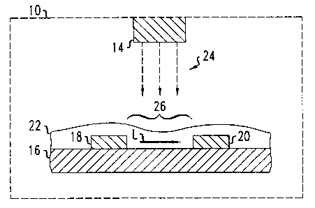
Figure 1 is a cross-sectional view of an optically controlled switch;
Figure 2 shows a control circuit based on the optically controlled switch of
Figure 1;
Figure 3 is a flow chart for a method of operating the optically-based control
circuit of Figure 2; and
Figure 4 is an oblique view of a micro-electromechanical (MEM) device that
uses the optically-based control circuit of Figure 2.
In the Figures, like reference numbers refer to functionally equivalent
elements or features.
DETA1LED DESCRIPTION OF THE EMBODIMENTS
Figure 1 shows an optically controlled switch 10. The switch l0 includes a
photosensitive switch 12 and a light source 14. The photosensitive switch 12
is based
on a planar structure. The planar structure includes an insulating substrate
16, two
electrodes 18, 20 located on the substrate 16, and a photosensitive layer 22
that
overlays both electrodes 18, 20 and the substrate 16. The light source 14
produces
light with a wavelength that is adapted to change the resistivity of the
material in the
photosensitive layer 22.
In the planar topology, the thickness of photosensitive layer 22 is less than
the
length of channel region 26. Also, light source 14 transmits light in a
direction
transverse to the conduction direction, L, in channel region 26. Thus, the
light is able
to penetrate the entire length of the channel region 26 even if the channel
region 26 is
long.
For switch-like behavior, the ratio of the resistance of channel region 26
when
illuminated, i.e., bright state; to the resistance of the channel region 26
when not
illuminated, i.e., dark state, must be at least 104, preferably is at least
106, and more
preferably is 108 or more. To obtain such a high ratio of resistances, the
entire length
of the channel region 26 must illuminated by tight source 14 in the bright
state. If a
.small transverse section along the channel region 26 remains insulating in
the bright
state, the resistance of that portion will dominate the entire channel
resistance,
because the resistivity of the channel material is orders of magnitude larger
in the
insulating state than in the conducting state. Thus, if a small section along
the length
of the channel region 26 remains non-illuminated, the ratio of the dark-state
resistance
CA 02380824 2002-04-08
Bao 22-55-18-3-95-1 3
to the bright-state resistance will not have the larger values characteristic
of switch
behavior.
This should be comrasted with a stacked topology common to solar cells (not
shown). In a stacked topology, incident tight propagates along the direction
of current
flow in the channel region. The length of the channel region must be short if
light is
to penetrate the entire length of the channel region.
In the planar topology, channel region 26 may be as long as desired without
interfering with the ability of light source !4 to illuminate the entire
channel region
26. In contrast with the stacked topology, the planar topology enables the
channel
length to be long enough to provide a high channel breakdown voltage without
interfering with the need for the whole channel region 26 to be conducting in
the
bright state. Exemplary breakdown voltages for channel region 26 are at least
50
volts, preferably at least 100 volts and more preferably at least 300 volts.
The planar topology also allows channel region 26 to have a dark-state
electrical resistance characteristic of switch behavior, i.e., due to the long
channel
length: Exemplary channel regions 26 have dark-state resistances of at least
10'
ohms, preferably at least 10a ohms, and more preferably 109 ohms or more.
These
large resistances insure that photosensitive switch 12 has a very low leakage
current
in the dark state.
2 0 In Figure 1, the electrodes 18, 20 are made of gold (Au), aluminum (AI),
indium-tin-oxide, titanium nitride (TiN), heavily doped silicon, or other
conductors.
In preferred embodiments, both electrodes 18, 20 are made from the same
conductor
so that illumination does not photovoltaically produce a voltage across
channel region
26.
The material of photosensitive layer 22 has a resistivity that responds to
light
in a preselected wavelength range. When not illuminated, the photosensitive
layer 22
is a good insulator, and when illuminated, the photosensitive layer 22 is a
fairly good
conductor. For channel region 26, the ratio of the resistance in the dark
state to the
resistance in the light state is significantly higher than for inorganic
semiconductors.
The photosensitive layer 22 includes an organic matrix that is doped with an
appropriate electron donor or acceptor to produce a material that conducts
when
suitably illuminated.
CA 02380824 2002-04-08
Bao 22-55-18-3-95-1 4
Exemplary organic materials for photosensitive layer 22; include conjugated
organic oligomers and polymers such as derivatives of oligomers and polymers
containing aromatic units such as phenylenevinylenes, fluorenes, thiophenes,
and
pyrroles. Exemplary oligomers and polymers of phenylenevinyienes have
substitutions of alkoxyl or cyano groups off the main chains. Some matrices
include
copolymers and blends of one or more of the above-described conjugated organic
oligomers and polymers.
Preferred organic materials are fully conjugated oligomers and/or polymers
that are molecularly aligned to increase the conductivity between electrodes
18, 20
when suitably illuminated. The preferred alignments increase inter-molecular
overlaps to provide higher charge mobilities when suitably illuminated, e.g.,
mobilities of about 10'~ cm2lvolt-second or more. The matrix molecules may be
aligned by stretching a matrix film prior to deposition, quenching the matrix
to a
liquid crystal state from a liquid state, or depositing the matrix on an
alignment layer.
Exemplary dopants for organic matrices include organic oligomers and
polymers, inorganic nanocrystals, and organo-metallic complexes. The dopants
are
either miscible in the organic matrix or chemically bound to the matrix
molecules.
Upon illumination, the dopants function as either electron donors or electron
acceptors for the matrix, which would otherwise be an insulator.
2 0 The systems of dopants and matrix molecules belong to one of tvvo classes.
In
the first class, the dopants are acceptors of photo-excited electrons from the
organic
matrix or donors of photo-excited holes to the matrix. In the second class,
the dopants
are photo-excitable donors of electrons to the organic matrix or acceptors of
photo-
excited holes from the matrix. Photo-excitations can result from the
absorption of
2 5 light by either the matrix molecules or dopants. Each class involves a
particular
alignment between highest occupied molecular orbitals (HOMOs) and lowest
unoccupied molecular orbitals (LUMOs) of the dopants and matrix molecules.
In the first class, the HOMO of the matrix molecules has a higher energy than
the HOMO of the dopants, and the LUMO of the matrix molecules also has a
higher
30 energy than the LUMO of the dopants. For this alignment of energy levels,
dopants
have higher electron affinities and higher ionization potentials than matrix
molecules.
Exemplary of this class are systems in which the matrix includes
poly(dialkoxyphenylenevinylene)s and the dopants are selected from C6o, metai-
CA 02380824 2002-04-08
Bao 22-55-18-3-95-1 5
phthalocyanines, thia-pyrylium; squarylium, azo-compounds, perylene,
anthanthrone,
and nanoerystalline CdSe.
In the second class, the HOMO of the matrix molecules has a lower energy
than the HOMO of the dopants, and the LUMO of the matrix molecules also has a
lower energy than the LUMO of the dopants. For this orbital alignment; the
dopants
have lower electron affinities and lower ionization potentials than the matrix
molecules. Exemplary of the class are systems where the matrix~includes
poly(a;a'-
dicyanophenylenevinylene)s and the dopants are
poly(dialkoxyphenylenevinylene)s.
In photosensitive layer 22, dopant concentrations are fixed to produce desired
conductivities when suitably illuminated by light source 14. Preferred
conductivities
result from between about 10'9 and about 10z' mobile charge carriers per
centimeter
cubed when suitably illuminated. To achieve such charge carrier
concentrations,
organic materials include. significant volume fractions of dopants. The volume
fraction occupied by dopants is typically greater than 0.1 percent, preferably
at least
I .0 percent, and often l0 percent or more.
Light source 14 excites electrons either from dopant sites to the matrix or
from
the matrix to dopant sites to convert photosensitive layer 22 from an
insulating state to
a conducting state: Thus, the conductivity of photosensitive layer 22 depends
on both
the dopant density and the illumination intensity from the light source 14:
The
dependencies of the conductivity on the dopant density and the illumination
intensity
are often approximately linear.
The conductivity of channel region 26 vanes linearly with both the channel
width and the inverse of the channel length. A preselected dark-state
resistance fixes
the ratio of the width to length of the channel region 26. The dark-state
resistance
2 5 determines the leakage current through the photosensitive switch 12. A
desired
minimum breakdown voltage determines the minimum length for the channel region
26 of the photosensitive switch 12.
A person of skill in the art could determine suitable channel dimensions and
dopant fractions based on presetected values of the dark-state and light-state
channel
resistances, the intensity of light source 14, and the channel breakdown
voltage.
Figure 2 shows a control circuit 34 based on optically controlled switch 10 of
Figure 1. The control circuit 34 includes a direct current (DC) voltage source
36 and
a voltage divider 38. In the voltage divider 38, the optically controlled
switch 10 and
CA 02380824 2002-04-08
Bao 22-55-18-3-95-1 6
a fixed resistor 40 connect in series. The fixed resistor 40 is a voltage
source for a
load element 42, e.g., a capacitor or inductor. The resistance of the
optically
controlled switch 10 controls the current through the fixed resistor 40 and
thus, the
voltage drop applied across the load element 42.
The optically controlled switch 10 includes light source 14 and photosensitive
switch 12 of Figure 1. Exemplary light sources I4 include light emitting
diodes
(LED) and diode lasers. The light source 14 may include an optical waveguide,
e.g:,
an optical fiber, that delivers light from a remote source to the
phot(isensitive switch
12. A voltage, V, used to modulate the light source 14 controls the resistance
of
photosensitive switch 12.
Figure 3 is a flow chart for a method 44 of controlling a circuit via an
optically
controlled variable switch, e.g., switch 12 of Figure 3: The method 44
includes
applying an external voltage across a photosensitive switch located in the
circuit (step
46). The method 44 also includes modulating the intensity of a light source,
e:g, light
source 14 of Figure'2, that illuminates the photosensitive organic resistor
while the
external voltage is applied across the photosensitive organic switch (step
48): The
modulated light intensity changes the resistance of the photosensitive switch
and thus,
the current that the external voltage produces in the circuit. The changed
current
changes the voltage drop across a load element, e.g., load element 42 in
Figure 2.
2 0 The induced change in the voltage drop across the photosensitive switch is
greater than any photovoltaic voltage induced across the photosensitive
switch.
Preferably, the change in the voltage drop is at least ten times any produced
photovoltaic voltage.
Referring again to Figure 2, exemplary control circuit 34 functions as a
digitally modulated (DM) voltage source for load element 42. In the D1VI
voltage
source, light source 14 functions as an optical modulator that produces a
repeating
sequence of bright and dark periods, e.g., ON and OFF periods of a diode laser
or
LED. The relative lengths of the bright and dark periods are varied to apply
different
average voltages across fixed resistor 40 and load element 42.
Figure 4 shows a micro-electromechanical (MEM) device 50 controlled by
control circuit 34 of Figure 3. The MEM device 50 includes a flexible stalk 5?
and a
top piece 54: The stalk 52 connects the top piece 54 to substrate 16. The cop
picre a.i
includes a first plate 56 of a capacitor and a reflector 58. A second plate 60
of the
CA 02380824 2002-04-08
Bao 22-55-18-3-95-1 7
capacitor is located on the substrate 16. The capacitor is load element 42 of
the
control circuit 34 shown in Figure 3. The control circuit 34 determines the
charge
state of the capacitor thereby controlling the orientation of the reflector 58
on the
MEM device 50.
The control circuit 34 functions as a DM voltage source for charging the
capacitor that controls the orientation of MEM device 50. In the DM voltage
source,
light source 14 shines a light beam with a modulated intensity on
photosensitive
resistor 12. The.light intensity is modulated at a frequency that is higher
than the time
constant for mechanical resonance in the MEM device 50, e.g., at least 5 - 10
times
the mechanical resonance frequency. At such high frequencies, the average
charge on
plates 56, 60 determines the mechanical reaction of MEM device 50 to the
driving
voltage. The average charge on the-plates 56, 60 depends on the relative
lengths of
the bright and dark portions of the illumination cycle.
Digital modulation of light source 14 requires a high frequency voltage
source,
V. The voltage source, V, can be a digital source, but the voltage source, V,
typically
has a maximum amplitude that is much smaller than that of the voltage
modulating
the charging and discharging ofthe capacitor ofMEM device 50. The voltage
applied
to capacitor is typically in the range of0 volts - 1000 volts and is
preferably in the
range of about 100 volts - 300 volts: For such high voltages, electrically
controlled
DM voltage sources are often more expensive than the optically controlled DM
voltage source formed from control circuit 34 and DC voltage source 36 of
Figure 3.
An exemplary DC source 36 has a voltage of about 100 - 300 volts. For such
a source a dark-state resistance of about 10~° ohms is preferable to
avoid substantial
power dissipation in the dark-state: For such a resistance, channel region 26
typically
has a length of at least 0.5 microns and preferably a length of 1 - 100
microns and a
width of about 1,000 microns. The channel region 26 is highly inter-digitated
to
reduce to overall transverse extend of the region 26 (Figure 4). Such channel
dimensions also provide breakdown voltages of in excess of 150 volts.
In other embodiments of system 50, photosensitive switch 12 is replaced by a
3 0 photosensitive resistor (not shown). The photosensitive resistor has a
photosensitive
channel region 26 that includes either organic or inorganic materials.
Exemplary
inorganic materials include amorphous selenium (Se), silicon ($i), cadmium
sultide
CA 02380824 2002-04-08
Bao 22-55-18-3-95-1 8
(CdS), and cadmium selenide (CdSe). These inorganic materials may be doped
with
well-known electron acceptors or donors.
Other embodiments of the invention will be apparent to those skilled in the
art
in light of the specification, drawings, and claims of this application.