Note : Les descriptions sont présentées dans la langue officielle dans laquelle elles ont été soumises.
CA 02381841 2002-04-15
- 1 - 01/047 mm
Power-electronic circuit arrangement, and a method for
transmitting real power
DESCRIPTION
Technical Field
The invention relates to the field of power
electronics. It relates to a power-electronic circuit
arrangement for transmitting real power as claimed in
the precharacterizing clause of patent claim l, and to
a method for operating a power-electranic circuit
arrangement as claimed in the precharacterizing clause
of patent claim 7.
Prior Art
A circuit arrangement such as this is known, for
example, from DE-A-196 15 855. This circuit. arrangement
has a first power converter, which is connected to a DC
voltage source having a first intermediate-circuit
capacitor voltage and has three load connections, as
well as second power converters, which are connected
between the load connections and AC voltage-side
connections for a load. At least one second
intermediate-circuit capacitor voltage or, if not, zero
volts, can be added to or subtracted from a voltage at
the respective load connection, by means of one of the
second power converters. In this case, the second
intermediate-circuit c<~pacitor voltage is less than the
first intermediate-circuit capacitor voltage. This
makes it possible to achieve a voltage graduation,
which is finer than that of the first
CA 02381841 2002-04-15
- 2 - 01/047 mm
intermediate-circuit capacitor voltage, for a voltage
at the AC voltage-side connections or across the load.
A predetermined mean voltage is set at the AC voltage-
side connections by the first power converter roughly
setting a voltage value in the vicinity of the
predetermined voltage, and the second power converter
adjusting any remaining difference with respect to the
predetermined voltage by pulse duration modulation. In
this case, the second. power: converter is clocked at a
1.0 faster rate than the first. The second power converters
are each fed by means of their own converters and a
joint supply transformer. DE-A 19T 20 787 describes a
method which avoids any feedback of power from the
second power converters so that the corresponding
converters for supplying the second power converters
may be pure rectifiers, that is to say they do not need
to have any feedback capability and are thus cheaper.
However, both cited cases involve complexity for
supplying the second power converters.
Description of the Invention
One object of the invention is to provide a
power-electronic circuit arrangement for transmitting
real power of the type mentioned initially, which has a
simpler design, and to provide a method for operating
this circuit arrangement.
These objects are achieved by a power-electronic
circuit arrangement for transmitting real power having
the features of patent claim 1, and by a method for
operating a power-electronic circuit arrangement having
the features of patent claim 7.
3~i The circuit arrangement according to the invention for
transmitting real power has a first power converter and
at least one second power converter, with the at least
one second power converter not having its own power
CA 02381841 2002-04-15
- 3 - 01/047 mm
supply means. Thus, in addition to the connections for
the respective load connections of the first power
converter and for the respective AC voltage-side
connection, the at least one second power converter has
no further connections or means for transmitting real
power or real energy to or from the second DC voltage
intermediate circuit.
There is thus no need for the initially mentioned
rectifiers for supplying the second power converters,
as a result of which the circuit arrangement becomes
considerably simpler, cheaper and mare reliable.
In one preferred embodiment, the circuit arrangement
according to the invention has a regulating device for
joint regulation of at least one intermediate-circuit
capacitor voltage of the at least one second power
converter, and of a common-mode voltage at the AC
voltage-side connections of the circuit arrangement, as
well as means for driving semiconductor switches in the
first power converter and in the at least one second
power converter on the basis of output variables from
this regulating device.
This makes it possible to keep mean values, over time,
of the voltages of the intermediate-circuit
capacitances of the at least one second power converter
and, possibly, of the first power converter essentially
constant, even though the second power converters are
interchanging real power with a load and with the first
power converter.
In a further preferred embodiment of the invention, a
second power converter is in each case connected in
3!~ series between a load. connection of the first power
converter and the associated AC voltage-side
connection, with these second power converters each
having two two-point inverter bridges. Nominal voltages
CA 02381841 2002-04-15
- 4 - 01/047 mm
of the intermediate-circuit capacitors in the first
power converter and in the second power converters
preferably have a ratio of 2:1 or 3:1. A voltage at the
AC voltage-side connections can thus be adjusted with a
graduation of 5 to 9 steps, as is shown in the
following table:
First power Second power Voltage Number of
converter _c_o_nverte~r ratio steps
2 point 2 point 2:1 5
2 point 2 point 3:1 6
3 point 2 point 2:1 7
3 point 2 point 3:1 9
In a further preferred embadiment of the invention, a
second power converter is in each case connected in
series between a load connection of the first power
converter and the associated AC voltage-side
connection, with these second power converters each
having a two-point inverter bridge and a three-point
inverter bridge. ' Nominal voltages of the
intermediate-circuit capacitors in the first power
converter and in the second power converters preferably
have a ratio of 2:1, 3:1, 4:1 or 5:1. The voltage at
the AC voltage-side connections can thus be adjusted
with a graduation of 7 to 15 steps, as shown in the
following table:
First Second Voltage Number of
power power ratio steps
converter converter
2 point 2/3 point 2:1 7
2 point 2/3 point 3:1 8
2 point 2/3 point 4:1 9
2 point 2/3 point 5:1 10
3 point 2/3 point 2:1 9
3 point 2/3 point 3:1 11
3 point 2/3 point 4:1 I 13
3 point 2/3 point 5:1 15
In a further preferred embodiment of the invention, two
2!5 second power converters are in each case connected in
CA 02381841 2002-04-15
- 5 - 01/047 mm
series between a load connection of the first power
converter and the associated AC voltage-side
connection, with these second power converters each
having two two-point inverter bridges. The voltage at
the AC voltage-side connections can thus be adjusted
with a graduation from 7 up to a maximum of 27 steps.
Nominal voltages of the intermediate-circuit capacitors
in the first power converter and in the second power
converters preferably have a ratio of 4:1:1, 5:1:1,
6:2:1, 7:2:1, 8:3:1 or 9:3:1.
In the method according to the invention, at least one
voltage of at least one intermediate-circuit
capacitance of the at least one second power converter
and a common-mode voltage of the AC voltage-side
connections of the circuit arrangement are regulated by
means of joint regulation. In one preferred variant of
the invention, the joint regulation also takes account
of a voltage of the intermediate circuit in the first
power converter, in particular a neutral point voltage
in the intermediate circuit. The joint regulation
influences the regulated voltages, taking account of a
joint optimization criterion.
In one preferred variant of the invention, a weighted
sum of the squares of the errors between the regulated
voltages and a respective nominal value is minimized.
Further preferred embodiments can be found in the
dependent patent claims.
Brief Description of the Drawings
The subject matter of the invention will be explained
in more detail in the following text with reference to
preferred exemplary embodiments, which are illustrated
in the attached drawings, in which:
CA 02381841 2002-04-15
- 5 - 01/047 mm
Figure 1 shows a circuit diagram of a circuit
arrangement according to the invention, in
conjunction with a load and a supply;
Figure 2 shows a second embodiment of a first power
converter;
Figure 3 shows a second embodiment of a second power
converter;
Figure 4 shows a series circuit of two second power
~_0 converters per load connection, according to
a further embodiment of the invention;
Figure 5 shows a control diagram of regulation
according to the invention in conjunction
with a circuit arrangement according to the
~.5 invention;
Figure 6 shows a control diagram of regulation
according to the invention in conjunction
with a further embodiment of the circuit
arrangement according to the invention;
a:0 Figure 7 shows an equivalent circuit, corresponding to
one phase o:f a circuit arrangement according
to the invention;
Figure 8 shows a profile of converter voltages; and
Figure 9 shows a profile of modulation levels of
25 converter bridges.
The reference symbols used in the drawings, and their
meanings, are listed in summary form in the List of
Reference Symbols. In principle, identical parts in the
?.0 figures are provided with the same reference symbols.
Approaches to Implementation of the Invention
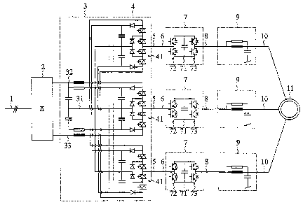
Figure 1 shows a circuit arrangement according to the
35 invention, in conjunction with a load and a supply. The
circuit arrangement is used for transmitting real power
from a DC voltage side to at least two AC voltage-side
connections 10, or vice versa. The DC voltage side is,
CA 02381841 2002-04-15
- 7 - 01/047 mm
for example, a first DC voltage intermediate circuit 3.
This has a first intermediate-circuit capacitor
voltage, a first positive pole 32 and a first negative
pole 33, and is fed by a rectifier 2, normally via a
network transformer 12, from a power supply network 1.
The rectifier 2 is preferably a converter' with a feed
back capability, that. is to say it has the capability
to transmit power from the first DC voltage
intermediate circuit :3 into the power supply network 1.
:LO In another embodiment of the invention, the rectifier 2
is a diode rectifier, that is to say without any
feedback capability.
The circuit arrangement according to the invention
:15 comprises a first power converter 4, which is connected
to a DC voltage source or to the first DC voltage
intermediate circuit 3. The first converter 4 is a
three-point inverter, as shown in Figure 1, or a
two-point inverter, as shown in Figure 2. The first
:~0 power converter 4 has at least two load connections 5.
The first power converter 4 preferably has a main
converter bridge 41 for each load connection. If the
first power converter 4 is a three-point inverter, the
first DC voltage intermediate circuit 3 has a first
25 neutral point 31. At least either the positive first
intermediate-circuit capacitor voltage, the negative
first intermediate-circuit capacitor voltage or, in the
case of a three-point inverter, zero volts can be
connected to each of the load connections 5 by means of
30 the main power converter bridges 41, using the first
power converter 4.
The circuit arrangement according to the invention
comprises at least one second power converter 7, which
35 has a second DC voltage intermediate circuit 71 with a
second intermediate-circuit capacitor voltage, which is
connected in parallel with a first and a second
converter bridge 72, 73. The at least one second power
CA 02381841 2002-04-15
- 8 - 01/047 mm
converter 7 is connected to one of the load connections
via a first bridge connection 6 of the first
converter bridge 72, and is connected to an AC voltage
side connection 10 via a second bridge connection 8 of
5 the second converter bridge 73.
In one preferred embodiment of the invention, a
sine-wave filter or filter 9 for smoothing a load
current or a load voltage is in each case connected
:LO between a second bridge connection 8 and an associated
AC voltage-side connection 10. A :Load 11, for example
an electrical machine, is connected to the AC voltage-
side connections 10. 'rhe power converters or their main
power converter bridges 41, first converter bridges 72
:l5 and second converter bridges 73 have semiconductor
switches, for example, IGCTs (Integrated Gate
Commutated Thyristors) or IGBTs (Insulated Gate Bipolar
Transistors).
:?0 Figure 2 shows a second embodiment of a first power
converter 4 and a first DC voltage intermediate circuit
3. In this case, th.e first power converter 4, the
two-point power converter and the intermediate circuit
3 are integral.
~; 5
Figure 3 shows a second embodiment of a second power
converter 7. In this embodiment, the second DC voltage
intermediate circuit 71 is in two parts, with a second
neutral point 74, and the second converter bridge 73 is
~~0 in the form of a three-point inverter. This embodiment
of the second power converter 7 is referred to as a
2/3-point power converter. Either the second
intermediate-circuit capacitor voltage, twice the
second intermediate-circuit capacitor voltage or zero
35 volts can thus be added to or subtracted from the
voltage at the corresponding load connection 5. In a
further variant, the first converter bridge 72 is also
in the form of a three-point inverter. In principle,
CA 02381841 2002-04-15
- 9 - 01/047 mm
any desired combinations of two-point and three-point
inverters are possible, in particular the combinations
which are described and claimed in DE-A-196 15 855.
Figure 4 shows a series circuit of two second power
converters 7a, 7b per load connection, according to a
further embodiment of the invention. The second power
converters 7 are connected in series via their first
bridge connections 6 and second bridge connections 8. A
.L0 first bridge connection 6 of a first second power
converter 7a is thus connected to a load connection 5,
and a second bridge connection 8 of the first second
power converter 7a is connected to a first bridge
connection 6 of the second second power converter 7b,
and a second bridge connection 8 of the second second
power converter 7b is connected to a filter 9 or to an
AC voltage-side connection 10. In principle, the
various embodiments of second power converters 7a, 7b
described above can be combined with one another as
0 required, that is to say the first second and the
second second power converters are 2-point and/or
3-point and/or 2/3-point converters.
One or more of:
~ the positive second intermediate-circuit capacitor
voltage,
~ the negative second intermediate-circuit capacitor
voltage, or
~ zero volts
:30 can be added, by means of the at least one second power
converter (7), to a voltage value which is connected by
the first power converter (4) to its load connection
(5). In addition, twice the second intermediate-circuit
capacitor voltage can also be added or subtracted by
.35 means of a .three-point inverter. The added voltage is
applied to the secand bridge connection 8 or to the
corresponding AC voltage-side connection 10. The second
intermediate-circuit capacitor voltage is preferably
CA 02381841 2002-04-15
- 10 - 01/047 mm
different to the first intermediate-circuit capacitor
voltage, in order to allow finer voltage graduation
than a voltage graduation of the first power converter
4 at the AC voltage-side connections 10. This principle
of refined voltage graduation is explained further in
the initially mE~ntioned DE-A-196 15 855 and
DE-A 197 20 787. The majority of the output voltage,
that is to say the voltage at the AC voltage-side
connections 10, is formed by the first power converter
Ji_0 4, which is clocked slowly and is preferably equipped
with IGCTs (Integrated Gate Commutated Thyristors). The
lesser proportion of the output voltage is formed by
the second power converters 7, which are driven, for
example, using pulse duration modulation and are
~.5 equipped with IGBTs (Insulated Gate Bipolar
Transistors). The switching frequency of the first
power converter 4 i:~ at least approximately 50 to
300 Hz, while the switching frequency of the second
power converter 7 is at least approximately 300 to
~:0 1000 Hz. The fundamental frequency of the output
voltage is, for example, 0 to 60 or 300 Hz.
In one example of the design of the first DC voltage
intermediate circuit 3 for the arrangement as shown in
~;5 Figure 1, with a nominal intermediate-circuit capacitor
voltage of the first. power converter 4 of 2 kV and of
the second power converter 7 of 1 kV, the resultant
voltages at an AC voltage-side connection 10 with
respect to the first and neutral point 31 are produced
3.0 in accordance with the following table. The term
"nominal intermediate-circuit capacitor voltage" refers
to a voltage for which an intermediate-circuit
capacitor and the associated converter are designed. In
the case of a two-point inverter, this is the total
35 voltage across the intermediate circuit, while in the
case of a three-point inverter or an intermediate
circuit with two capacitors and a neutral point, it is
half the total voltage across the intermediate circuit.
CA 02381841 2002-04-15
- 11 - 01/047 mm
1S' power 2n power Resultant
converter at the converter, voltage, at the
load connection between the first second bridge
bridge connection connection 8 or
6 and the second at the AC
bridge connection voltage-side
8 connection 10
+2 kV +1 kV +3 kV
+2 kV 0 kV +2 kV
+2 kV -1 kV +1 kV
0 kV +1 kV
0 kV 0 kV 0 kV
0 kV -1 kV -1 kV
-2 kV +1 kV
-2 kV 0 kV -2 kV
-2 kV -1 kV -3 kV
The voltage ratio between the nominal voltages of he
5 first DC voltage intermediate circuit 3 and of the
second DC voltage intermediate circuits 71 is in this
case 2:1. The resultant voltage can thus be switched in
seven steps. The design is redundant, since in some
cases different switch combinations lead to the same
DLO resultant voltage. T:he following arrangement with a
voltage ratio of 3:1 has no redundancies and nine
switching steps:
1s power 2n power Resultant voltage
converter converter
+3 kV +1 kV +4 kV
+3 kV 0 kV +3 kV
+3 kV -1 kV +2 kV'
0 kV +1 kV +1 kV'
0 kV 0 kV 0 kV
0 kV -1 kV -1 kV
-3 kV +1 kV -2 kV
-3 kV 0 kV =3 kV
-3 kV -1 kV -4 kV
1.5 Owing to the greater number of switching steps and the
finer voltage graduation, non-redundant arrangements
are preferred.
CA 02381841 2002-04-15
- 12 - 01/047 mm
During the operation of the circuit arrangement
according to the invention, the second power converters
7 interchange real power with both the load 11 and the
first power converter 4. According to the invention,
the second power converters 4 do not have their own
means for supplying power to the second power
converters 7 or for drawing electrical power from the
second power converters 7. Thus, apart from the first
:LO bridge connection 6 and the second bridge connection 8,
they have no further connections or means for
transmitting real power to or from the second DC
voltage intermediate circuit 71. However, if a second
power converter 7 overall emits more power or real
.L5 power to the load 11 and/or to the first power
converter 4, its second intermediate-circuit capacitor
voltage falls. Conversely, the second
intermediate-circuit capacitor voltage rises, when,
overall, the second power converter 7 receives real
:?0 power from the load 11 and/or from the first power
converter 4.
According to the invention, the interchange of real
power between the first power converter 4 and the
25 second power converters 7 is regulated such that the
regulated voltages, that is to say the voltages on the
capacitances in the intermediate circuits, remain
approximately constant. Joint regulation, that is to
say joint regulation of all the power converters 4, 7
?.0 in this case detects the regulated voltages and drives
the power converters 4, 7 in a coordinated manner, so
as to satisfy an optimization criterion that covers the
power converters 4, 7. According to the invention, this
can be done by varying or regulating a common-mode
35 voltage at the AC voltage-side connections 10.
If the first power converter 4 is a three-point power
converter, the first DC voltage intermediate circuit 3
CA 02381841 2002-04-15
- 13 - 01/047 mm
has a first neutral point 31. The overall voltage of
the first DC voltage intermediate circuit 3 is
regulated, for example, by the rectifier 2 or, if using
a diode rectifier, is kept essentially constant without
regulation. The neutral point voltage at the first
neutral point 31 must, however, also still be kept
approximately constant. In one preferred variant of the
invention, the neutral point voltage of the first
intermediate circuit is therefore also regulated in
such a way, that i.s to say it is included as a
regulated voltage in the joint regulation.
The term "intermediate-circuit capacitor voltage"
refers to a voltage value which actually occurs across
an intermediate-circuit capacitor during operation.
This corresponds to either half the intermediate
circuit, or the entire intermediate circuit. The
neutral point voltage and the entire voltage of an
intermediate circuit with a neutral point are both
likewise referred to as intermediate-circuit capacitor
voltages. The term "regulated voltage" covers regulated
intermediate-circuit capacitor voltages and the
regulated common-mode voltage.
The following table shows the three voltage steps which
can be switched using a 2/3-point power converter as
shown in Figure 3:
15 power 2n power Resultant voltage
converter converter _
+2.5 kV +1 kV +3.5 kV
+2.5 kV +0..5 kV +3 kV
+2.5 kV 0 kV +2.5 kV
+2.5 kV -0..5 kV +2 kV
+2.5 kV -1 kV +1.5 kV
0 kV +1 kV +1 kV
0 kV +0.5 kV +0.5 kV
0 kV 0 kV 0 kV
0 kV -0.5 kV -0.5 kV
0 kV -1 kV -1 kV
-2.5 kV +1 kV -1.5 kV
CA 02381841 2002-04-15
- 14 - 01/047 mm
-2.5 +0..5 kV -2 kV
kV
-2.5 kV 0 kV -2.5 kV
-2.5 kV -0..5 kV -3 kV
-2.5 kV -1 kV -3.5 kV
The voltage ratio between the nominal voltages of the
first DC voltage intermediate circuit 3 and of the
second DC voltage intermediate circuit 71 is in this
case 5:1. The table shows 15 switching steps and no
redundancies. With a voltage ratio of 4:1, there are 13
different steps (2 redundant steps), and with a voltage
ratio of 3:1, there are 11 different steps (4 redundant
steps).
:L 0
If two second power converters 7 per load connection 5
are connected in series, the voltage steps which can be
switched are the same as those with a single 2/3-point
power converter as :shown in Figure 3, provided the
:L5 series-connected second power converters 7 have the
same nominal intermediate-circuit capacitor voltage.
If the nominal intermediate-circuit capacitor voltages
of series-connected second power converters 7 differ,
:?0 then up to 27 switching steps are possible. The
following table quotEa, for preferred embodiments of
the invention, the number of switching steps as a
function of the voltage ratios of the nominal
intermediate-circuit capacitor voltages of the first
25 power converter 4 (Ucm), of a first series-connected
second power converter 7 (Ucs1) and of a second
series-connected second power converter 7 (Ucs2).
Ucm:Ucs1_:U___cs2 Number of switching steps
~
4:1:1 __ 13
5:1:1 15
6:2:1 19
7:2:1 21
8:3:1 _ 25
9:3:1 27
CA 02381841 2002-04-15
- 15 - 01/047 mm
Both the use of three-point inverters in the second
power converters 7 and the series connection of a
number of second power converters 7 allow finer
graduation of the voltage at the AC voltage-side
connections 10 than the voltage graduation of the first
power converter 4. :In each case, the voltages of the
individual capacitances in the second power converters
7 are regulated by the joint regulation.
1.0 In summary, the joint regulation regulates the
regulated voltages, that is to say the voltages of the
intermediate-circuit capacitances of the second power
converters 7 and, possibly, of the first power
converter 4, in particular the neutral point voltage.
This is done by using suitable voltage measurement
equipment to determine measured values for the
regulated voltages.
Figure 5 shows a control diagram of regulation
~:0 according to the invention in conjunction with a
circuit arrangement according to the invention as shown
in Figure 1. The joint regulation according to the
invention operates as follows: higher-level load
regulation 52 detects one or more intermediate-circuit
~:5 voltage values 56 of the intermediate-circuit
capacitances in the first DC voltage intermediate
circuit 3, as well as output voltage values 53 at the
AC voltage-side connections 10. The higher-level load
regulation 52 presets load voltage nominal values 55
30 for an intermediate-circuit voltage regulator 51, which
nominal values 55 must be present, relative to one
another, at the AC voltage-side connections 10, in
order to drive the load 11 (which is, in particular, a
drive motor) in the desired manner. Presetting the
35 output voltage at the AC voltage--side connections 10
with a non-redundant design of the circuit arrangement
according to the invention results in the switches in
the power converters or a modulation level for pulse
CA 02381841 2002-04-15
- 16 - 01/047 mm
width modulation in the second power converters 7 being
produced unambiguously.
According to the invention, a common, so-called
common-mode, voltage is added to the load voltage
nominal values 55 for each phase in the
intermediate-circuit voltage regulator 51, in order to
influence the real power flow between the converters,
or in order to influence the regulated voltages for the
u0 intermediate-circuit c:apacitances. The sums of the load
voltage nominal values 55 and the common-mode voltage
are referred to as the modified load voltage nominal
values. The modified load voltage nominal values are
used, in the intermediate-circuit voltage regulator 51,
~_5 to define a modulation level 54 for the first power
converter 4 and modulation levels 57 for the second
power converters 7, so that the modified load voltage
nominal values are produced at the AC voltage-side
connections 10. This is done by measuring the voltages
20 of preferably all the intermediate-circuit capacitors
in the first power converter 4 and in the second power
converters 7, and by also processing them in the
intermediate-circuit voltage regulator 51.
c.5 The following terms are used: a maximum converter
output voltage is equal to the sum of the
intermediate-circuit capacitor voltages of the
series-connected first. and second power converters. A
drive level is equal to the ratio between the present
30 and the maximum converter output voltage for a
steady-state operating point in the entire converter,
with the amplitude of an output voltage fundamental
being regarded as the present converter output voltage.
The drive level is quoted as a percentage, from 0 to
35 100. A modulation .bevel is the ratio between the
instantaneous and the maximum converter output voltage.
This is defined for the instantaneous values of a phase
CA 02381841 2002-04-15
- 17 - 01/047 mm
voltage, for the entire converter or for one converter
element, and has a value between -1 and +1.
The common-mode voltage has no significant influence on
the load 11. However, it should be as small as possible
and should change slowly, in order to reduce, inter
alia, the voltage load on motor windings with respect
to ground potential. The only governing factors for the
behavior of the load 11 are the differences between the.
voltages at the AC voltage-side connections 10, also
referred to as the differential mode.
For this reason, the common-mode voltage offers one
degree of freedom for driving the load 11. According to
the invention, this degree of freedom is used to
influence the load flow between the converters and the
intermediate-circuit capacitor voltages. In this case,
instantaneous values of the intermediate-circuit
capacitor voltages cannot be controlled, and all the
:~0 that can be done is to regulate a mean value, over
time, of each intermediate-circuit capacitor voltage
over one fundamental cycle of the output 'voltages. The
full drive level of 100 cannot be achieved either,
since series-connected first and second power
:?5 converters 4, 7 would need to emit power continuously
to achieve this. The maximum drive level which can be
achieved is a value of approximately 82~ (amplitude of
the output voltage as a ratio of the sum of the
intermediate-circuit capacitor voltages of the
;30 series-connected first and second power converters 4,
7) .
The influence of the common-mode voltage on the
regulated voltages of the intermediate-circuit
;~5 capacitances depends on the respective operating point
of the circuit arrangement. The joint regulation, which
is preferably sampling regulation, therefore. has a
mathematical converter model of the first and second
CA 02381841 2002-04-15
- 18 - 01/047 mm
power converters 4, 7. This model describes a change in
the intermediate-circuit capacitor voltages as a
function of the common-mode voltage and of further
system variables, that is to say the predetermined load
voltages and preferably measured load currents per
phase:
U.; ~k~ _ -L; ~uh (k~, u',"or,.ef (k~~ imor (k~~C'.; j E ~Cnp, Ca, Cb, Cc~ ( 1
)
LI~~k+1~=U~~k~+U~~k~~at jE fCnp,Ca,Cb,Cc} (2)
In this case, [k] denotes the value of a variable at
the k-th considered time in the sampling regulation.
Estimated or calculated values are marked, in contrast
to measured or predetermined values, with an inverted-v
symbol such as that, for example, in U.
j E ~Cnp, Ca, Cb, Cc~ is an index of thE: capacitances
considered with the regulated intermediate-circuit
capacitor voltages, in particular with Cnp relating to
the voltage at the first neutral point 31, and Ca, Cb,
Cc relating to the voltages of the capacitances in the
second DC voltage intermediate circuits 71 of the
phases which are annoted a, b and c. Cnp is equal to
the sum of the two c:apacitances in the first DC voltage
intermediate circuit 3.
The variables are as follows:
~ uh is a variable which covers all possible values
Luh,min' ' ' 'uh,maxJ of the common-mode voltage,
~ umot,ref is a vector of the predetermined load
voltages,
~ imot is a vector of the load currents,
~ h is a vector of the estimated currents in the
capacitances under consideration,
~ C~ is a vector of the capacitances under
consideration,
CA 02381841 2002-04-15
- 19 - 01/047 mm
~ U~ is a vector of the voltages for the
capacitances under consideration,
~ U~ is an estimatE~d value of U~,
~ U~ is an estimated time derivative of U~ and
~ ~t is the duration of one sampling time step.
The process of determining h from uh[k] and uI"ot,ref [k]
and i~t[k] includes t:he major portion of the converter
model. The model is obtained in the following way, on
:10 the basis of an idealized consideration of the
converter:
For a circuit arrangement as shown in Figure 1, Figure
7 shows an idealized equivalent circuit of the
:15 rectifier 2, of the first DC voltage intermediate
circuit 3, of the first power converter 4 and of one of
the second power converters 7.
In the equivalent circuit, the converter bridges are
:?0 modeled as switches or_ changeover switches, and the two
intermediate-circuit capacitors in the first DC voltage
intermediate circuit 3 are combined to form an
equivalent capacitance Cnp of the first neutral point
31. A positive or negative intermediate circuit voltage
:?5 of the first DC voltage intermediate circuit 3 is +ua",
or -ua", respectively, and a voltage at the first
neutral point 31 is +u~,p. The switches in the main
power converter bridge 41 are driven with a modulation
level sm, using pulse width modulation. The modulation
:SO level sm assumes values between +1 and -1, with a
voltage um at the load connection 5, under
consideration, of the first power converter 4 being
equal to +ua" when s~" =- +1, and being equal to -u~, when
sm = -1. Corresponding values of um are
..5 linear-interpolated for intermediate values of sm.
CA 02381841 2002-04-15
- 20 - 01/047 mm
The second power converter 7 with an
intermediate-circuit capacitor voltage ups is driven
with a modulation .Level ss. The modulation level ss
assumes values between +1 and -1, with a voltage us
between the first bridge connection 6 and the second
bridge connection 8 of the second power converter 7
being equal to +u~s .for s$ = +1, and being equal to -ups
for s5 = -1. The modulation level s$ is composed of a
modulation level ssn of the first converter bridge 72
and a modulation Level ssp of the second converter
bridge 73, where
Ssp - Ssn
s5 =
2
In principle, for a given modulation level s5, any
desired values may be chosen for ssP and ssn, provided
they satisfy the above equation. However, ssn = -ssP is
preferably chosen. This results in the switching losses
and switched-on losses being distributed uniformly.
The carrier frequency for the pulse width modulation is
considerably higher than the fundamenta:L frequency of
an output voltage from the circuit arrangement, so that
the converters can be modeled as continuous apparatuses,
as described in the article "PWM-control of multi-level
voltage-source inverters", M. Veenstra and A. Rufer,
Proceedings of th.e Power Electronics Specialists
Conference, vol. 3, pp. 1387-1393, TEES, 2000.
Figure 8 shows a waveform of converter voltages for a
single phase for varying modulation levels of the first
power converter 4 and of the corresponding second power
converter 7. In this case, uph is the voltage at the
corresponding second bridge connection 8, that is to
say the sum of a voltage value um,Ph of the first power
converter 4 and a voltage value us,ph of the second power
converter 7. An additional index ph for said voltages
indicates that these are variables for_ one specific
CA 02381841 2002-04-15
- 21 - 01/047 mm
phase. The indicated voltages correspond to those from
the table above f.o:r the arrangement with a voltage
ratio of 3:1 with nine switching steps, normalized to a
maximum resultant voltage of 4 kV. Table values for the
voltage for the first power converter 4 are marked by
squares, table values for the voltage from the second
power converter are marked by circles, and table values
for the total voltage are marked by crosses. The
profile of the voltages between the table values is
determined by linear interpolation.
Figure 9 shows a profile of modulation levels for
converter bridges for producing the converter voltages
shown in Figure 8. This once again shows a profile of a
modulation level s"p at the first neutra:L point 31 and
snp is defined as t:he relative probability over time of
the first neutral point 31 being connected to the load
connection 5. snp is thus directly dependent on sm.
Values for snp of different phases are combined to form
a vector snP .
The curves in Figures 8 and 9 represent unique
relationships, which associate a pair of voltage values
um,phr us,Pn from the :first and second power converters 4,
7, as well as a group of three modulation levels sm, ss,
snp with each value uph of a voltage at a second bridge
connection 8 or at an AC voltage-side connection 10.
Using these modulation levels, the estimated currents
h into the intermediate-circuit capa~~itances under
consideration at the k-th time under consideration are
defined as
lkJ - lmot LkJ ~ Snp LkJ (3)
np
iC ~k~ _ -i ph ~k~ ss, ph ~k~ b'ph E {a, b, c~ (4)
s, ph
CA 02381841 2002-04-15
- 22 - 01/047 mm
Equation (3) means that a current in the equivalent
capacitance is equal to the sum of the load currents,
in each case multiplied by the modulation level snp at
the first neutral point 31 with respect to the phase of
the respective load current. Equation (4) means that,
for each phase a,b,c in a three-phase system, a current
in the intermediate-circuit capacitance of the second
power converter 7 for the relevant phase is determined
from the load current iph in that phase, multiplied by
the modulation level ss,ph of the second power converter
7 in that phase.
Equations 2 and 5 use k+1, since this is a prediction
of the capacitor voltages for the next sampling time.
Equations 3 and 4 use k, since these are measured and
calculated currents and modulation levels to be set for
this sampling time. However, these values from
Equations 3 and 4 will not change, or will change only
insignificantly, i.n the time ini:erval up to the next
sampling time. Similar arguments apply to Equations
6-9.
Any error between the regulated intermediate-circuit
capacitor voltages and the predetermined, preferably
constant, ideal values U~,ref are
EU j = U j ~k + 1~- U j,,ef j E ~Cnp, Ca, Ch, Cc ~ ( 5 )
The regulation is intended to keep these voltage errors
as small as possible. The common-mode voltage and the
rate of change izh of the common-mode voltage should
likewise be kept as small as possible.
uh = uh (kl (6)
u,, =~u,~~k~-u,,~k-1DlOt (7)
This is done by forming a cost function, by summation
of the squares of the above errors:
CA 02381841 2002-04-15
- 23 - 01/047 mm
K~uh ~kD - kuh ~us )z + ka"r~ lun ~2 '~' ~, ~~U.i ~ ,~ E ~CnP~ L'a~ C'b~ Cc~
J
Weighting factors k"h and kdun vary the weighting of
errors in the common-mode voltage or its change in
comparison to errors in the regulated voltages. The
common-mode voltage which is chosen is that which
minimizes the cost function.
u~' 'k' ~ ~h 'k' ~K~uh~k~~'min(K)
A known minimization method is used to minimize the
cost function. Methods such as these are implemented,
for example, with an optimization "Toolbox" in the
mathematical softwa.r~e packet MATLABTM from The MathWorks
Inc.
Thus, in the optimization process, that common-mode
voltage is selected which minimizes a weighted sum of
the squares of the errors between the regulated
voltages and a respective nominal value. The weighting
factors kuh and kd"h are such that the
intermediate-circuit capacitor voltages are regulated,
averaged over time, at essentially constant values, and
a variation in the common-mode voltage of., for example,
a maximum of approximately 30% of the maximum converter
output voltage is permissible.
During practical operation, the instantaneous values of
the voltages of the capacitances oscillate by up to
approximately loo around the nominal voltage of the
respective capacitance.
The method according to the invention thus comprises
the following steps:
a) Presetting ui"ot,ref [k] by higher-level regulation
52, 59.
b) Measurement of i~,ot [k]
CA 02381841 2002-04-15
- 24 - 01/047 mm
c) Prediction of a change in the regulated
intermediate-circuit capacitor voltages as a
function of the common-mode voltage and of further
system variables by means of a converter model of
sampling regulation at a first sampling time. This
is done by determining U~ in accordance with
Equation ( 1 ) i.n that
1. uh[k] is predetermined by means of the
optimization method,
2 . umot,ref [ k] and u,, [ k] are added, which results in
the modeled output voltage uph for each phase,
3. Modulation levels sm, s5, s~P are determined for
each phase, :in accordance with the
relationships shown in Figures 8 and 9,
4. The estimated currents h in the intermediate
circuit capacitances under consideration are
determined using Equations (3) and (4),
5. The estimated time derivative of ITj of U~ is
determined using Equation (1), and
6. The change u~[k] ~ Ot in U~ and the new estimated
value u~[k + 1] are determined using Equation
(2) .
d) Determination of a common-mode voltage which
minimizes the cost function in accordance with
Equations (5-8'.) at at least one next sampling
time, by means of an optimization process. Step c)
is carried out repeatedly, with uh [ k] being varied
by means of the optimization method.
e) Addition of the optimized common-mode voltage,
determined in step d), to load voltage nominal
values 55, 58 (which are determined for driving
the load) at 'the AC: voltage-side connections 10,
thus resulting in modified load voltage nominal
values for the respective AC voltage-side
connections 10,,
f) Driving or modulation of the first power converter
Q and of the at least one second pcwer converter 7
CA 02381841 2002-04-15
_ - 25 - 01/047 nun
on the basis of these modified load voltage
nominal values.
If the circuit arrangement does not have any redundant
switching states, the regulation according to the
invention results in t:he regulated voltages oscillating
about the nominal value. The regulation :in this case
stabilizes the mean values of the voltages over one
fundamental cycle, and minimizes the amplitude of the
voltage oscillations, which is sufficient for operation
of the circuit arrangement. The amplitudes of the
oscillations depend on the values of the respective
capacitances and on the real power being transmitted.
By way of example, for a converter with a rating of
1.4 MVA and with capacitor voltages of 3 and 1 kV, this
results in a voltage ratio of 3:1 and nine switching
steps, with the capacitance of the first DC voltage
intermediate circuit 3 being a total of 775
microfarads, and the capacitance of one individual
second power converter 7 in each case being 4650
microfarads, and with the neutral point voltage and the
intermediate-circuit capacitor voltages of the second
power converters 7 each oscillating by a maximum of 10$
about their nominal values. In this case, an energy
storage capacitance in the first DC voltage
intermediate circuit 3 amounts to a total of 5 Ws/kVA,
and an energy storage capacitance for all the second
power converters 7 likewise amounts to a total of
5 Ws/kVA. The variation of the common-mode voltage is a
maximum of about 30~ of the maximum converter output
voltage.
The circuit arrangement according to the invention is
suitable for new systems, but is also suitable for
retrofitting existing drives. In order to protect a
drive against the increased common-mode voltage, the
end winding insulation is improved, for example, by
spraying on corona-discharge protection.
CA 02381841 2002-04-15
- 26 - 01/047 mm
For load voltage frequencies which are below a nominal
frequency, the amplitude of the load voltage is also
reduced in a known manner for supplying a motor. The
regulation of the intermediate-circuit capacitor
voltages at the AC voltage-side connections 10 becomes
more difficult at these lower voltages. In this case,
the optimization of the regulation preferably takes
into account a prediction of the converter response
:10 over two or more sampling steps. The cost function in
this case includes the sum of the squares of the errors
under consideration for each of the sampling steps.
Appropriate optimization methods are known from the
field of model predici~ive control.
:L 5
In one preferred variant of the invention, the cost
function also has at least one term with the time
integral of one of the voltage errors under
consideration. This eliminates any steady-state error
20 between the corresponding voltage and its nominal
value.
The method according to the invention is adapted as
appropriate for other variants of the circuit
:?5 arrangement. For example, if the first power converter
4 is a two-point power converter, the term EUNP is
eliminated from the cost function.
In a further embodiment of the invention, the circuit
.30 arrangement according to the invention is arranged
between the power supply network 1 and the first DC
voltage intermediate circuit 3, and is thus used mainly
as a rectifier, with feedback capability, for supplying
the first DC voltage intermediate circuit 3. In this
_s5 application, the joint. regulation regulates the overall
voltage of the first intermediate circuit instead of
the operating point for the load. The load currents i~t
CA 02381841 2002-04-15
- 2? - 01/047 mm
correspond in this case to network currents, and
network-side regulation 59 is used instead of the
higher-level load regulation 52.
Figure. 6 shows a control diagram of regulation
according to the invention in conjunction with this
further embodiment. ','he rectifier 2 and the network
transformer 12 are thus replaced by a further first
power converter 4' and a further second power converter
7'. AC voltage-side connections 10 of the further
second power converters 7' are connected to the power
supply network 1 without a transformer. The further
first and second power converters 4', 7' are driven by
means of a further modulation level 54' of the further
first power converter 4', or further modulation levels
57' of the further second power converters 7'. These
modulation levels are produced by a further
intermediate-circuit voltage regulator 51' on the basis
of the network-side output voltage nominal values 58,
which are in turn produced by network-side regulation
59. The network-side regulation 59 governs the
network-side output voltage nominal values 58 on the
basis of measured intermediate-circuit voltage values
56 and network voltage values 60. The network-side
regulation 59 cannot influence the network voltage, but
controls the power flow into the first DC voltage
intermediate circuit :3 so that its overall voltage is
kept essentially constant.
The power supply network 1 has a constant voltage and
frequency, which correspond to the rated operating
point of the further first power converter 4' in
conjunction with the further second power converter 7'.
These are thus always operated at least approximately
at this operating point, in which case the network-side
common-mode voltage can be kept very low by means of
the further intermediate-circuit voltage regulator 51',
CA 02381841 2002-04-15
- 28 - 01/047 mm
for example at a maximum of 5$ of the maximum converter
output voltage.
Voltages from preferably all the intermediate-circuit
capacitors in the further first power converter 4' and
in the further second power converters 7' are measured,
and are also processed in the further
intermediate-circuit voltage regulator 51'.
7.0 If the circuit arrangement is arranged between the
power supply network 1 and the first DC voltage
intermediate circuit 3, the frequency of the voltages
at the AC voltage-side connections 10 corresponds to a
constant network frequency. In this case, the
~.5 common-mode voltage is very low, that is to say it is a
maximum of approximately 5~ of the maximum converter
drive level.
In summary, the intermediate-circuit voltage regulator
~;0 51 regulates the neutral point voltage . o~ the first DC
voltage intermediate circuit 3, the
intermediate-circuit capacitor voltages of the second
power converters 7 and the common-mode voltage at the
load 11, and the further intermediate-circuit voltage
c'.5 regulator 51' regulates the neutral point voltage of
the first DC voltage intermediate circuit 3, the
intermediate-circuit capacitor voltages of the further
second power converter's 7', and the common-mode voltage
with respect to the network 1.
There are various options for regulating the neutral
point voltage of the' first DC voltage intermediate
circuit 3, as follows:
1. The first DC voltage intermediate circuit 3 has
two independent neutral points, that is to say
neutral points which are not connected, with one
neutral point on the network side and one on the
CA 02381841 2002-04-15
~ - 29 - 01!047 mm
load side. As i:n the case of a diode rectifier,
the power is transmitted only via the first
positive pole :32 and the first negative pole 33.
Each side regulates its own neutral point voltage.
2. Only one of the two sides regulates a common
neutral point voltage, and the other side does not
consider this in the optimization process.
3. Both sides consider the neutral point voltage and
try to prevent it from deviating too far from its
nominal value. By way of example, the neutral
point voltage is taken into account with a reduced
weighting in both optimization processes with the
result that it i.s not regulated excessively. The
weighting is different, for example, for the two
sides.
4. The circuit arrangement has a global
intermediate-circuit voltage regulator, which
minimizes a cost function including all the
intermediate circuit voltages and both common-mode
voltages in the entire circuit arrangement shown
in Figure 5.
:25
The further embodiment of the invention as shown in
Figure 5 allows the circuit arrangement to be used
without a network transformer, which means a major
simplification. The circuit arrangement according to
:30 the invention can, of course, also be used as only a
network-side circuit arrangement 7',4',3 with a DC
voltage load and without the load-side circuit
arrangement 4,7.
:35 If the second power converters 7 contain three-point
inverters and/or if a number of second power converters
7 are connected in series in each phase, then the cost
function correspondingly contains at least one
CA 02381841 2002-04-15
- 30 - 01/047 mm
additional term for each additional capacitance and for
each regulated voltage'.
If the circuit arrangement has redundancies, the
optimization process also takes account of redundant
switching states. Since, in this case, a predetermined
common-mode voltage does not uniquely correspond to a
single drive level for the converters, multidimensional
optimization is cart-ied out. This means that the
7.0 optimization process varies both the common-mode
voltage and the redundant switching states. In this
case, the optimization process reduces both the
common-mode voltage and the number of switching
processes, that is to say processes for switching
7.5 semiconductor switches on or off. In principle, in this
case, the redundant switching states mean that the
common-mode voltage can be reduced to a greater extent
and/or the number of switching processes can be
reduced. In order to minimize switching losses in one
c.0 preferred variant of the invention, the number of
switching processes is minimized, and the common-mode
voltage is allowed to vary.
CA 02381841 2002-04-15
- 31 - 01/047 mm
List of Reference Symbols
1 Power supply network
2 Rectifier
3 First DC-voltage intermediate circuit
4 First power converter
4' Further first power converter
5 Load connection of the first power converter
6 First bridge connection
=LO7 Second power converter
7' Further second power converter
7a First second power converter
7b Second second power converter
8 Second bridge connection
~~L59 Filter
AC voltage-side connection
11 Load
12 Network transformer
31 First neutral point
32 First positive: pole
33 First negative pole
41 Main converter bridge
51 Intermediate-circuit voltage regulator
51' Further intez~iediate-circuit voltage regulator
52 Higher-level load regulation
53 Output voltage values
54 Modulation level of the first power converter
54' Further modulation level of the further first
power converter
~~055 Load voltage nominal values
56 Intermediate-circuit voltage values
57 Modulation levels of the second power
converters
57' Further modulation levels of the further second
..5 power. converters
58 Network-side output voltage nominal values
59 Network-side regulation
60 Network voltage values
CA 02381841 2002-04-15
- 32 - 01/047 mm
71 Second DC voltage intermediate circuit
72 First converter bridge
73 Second converter bridge
74 Second neutral point