Note : Les descriptions sont présentées dans la langue officielle dans laquelle elles ont été soumises.
CA 02383949 2002-03-04
WO 01/18580 PCT/US00/24666
AN OPTOELECTRONIC ASSEMBLY AND METHOD FOR FABRICATING
THE SAME
FIELD OF THE INVENTION
The present invention relates generally to optoelectronic assemblies
having optical components and methods for making the same; more
particularly, the present invention relates to an assembly having optical
components mounted on a quasi-planar substrate and a flexure and methods for
making the same.
BACKGROUND OF THE INVENTION
Sealed packages are necessary to contain, protect, couple to optical fibers
and electrically connect optoelectronic components. Optoelectronics packaging
is one of the most difficult and costly operations in optoelectronics
manufacturing. Optoelectronic packages provide submicron alignment between
optical elements, high-speed electrical connections, excellent heat
dissipation,
and high reliability. Providing such features has resulted in optoelectronic
packages that are larger, costlier and more difficult to manufacture than
electronic packages. In addition, current designs of optoelectronic packages
and
associated fabrication processes are ill adapted for automation because
today's
high-performance butterfly packages are characterized by a large multiplicity
of
mechanical parts (submounts, brackets, ferrules, etc.), three-dimensional (3D)
alignment requirements, and poor mechanical accessibility.
U.S. Pat. No. 4,953,006 by Kovatz discloses a package for an edge-coupled
optoelectronic device. The package includes a cover with a window, so that
optoelectronic device, such as, for example, a laser, may be coupled to
external
optics, such as a lens or an optical fiber. Although this package provides
1
CA 02383949 2002-03-04
WO 01/18580 PCT/US00/24666
hermeticity and high-speed electrical connections, it does not provide for a
way
to mount and align collimation or coupling optics nor optical fibers.
U.S. Pat. No. 5,005,178 by Kluitmans and Tjassens and U.S. Pat. No.
5,227,646 by Shigeno also disclose packages for optical and optoelectronic
components. Kluitmans et al. discuss a package for a laser diode coupled to an
optical fiber. The package includes a conducting rod so that the laser may be
used at high speed. Shigeno describes a heat sink for cooling an enclosed
laser
diode, where the laser diode is preferably coupled to an optical fiber.
However,
in both of the above patents, it is difficult to align the laser diode with
the optical
fiber when constructing the package. Both designs use numerous parts in
complex three dimensional arrangements and are unsuitable for automated
assembly. U.S. Patent No. 5,628,196 by Farmer discloses a package including a
heat sink for a semiconductor laser, but provides no efficient means for
coupling
the laser to other optics.
The difficulty in alignment is made more problematic where welding is
involved in the manufacturing of a package. The result of the welding process
causes a shift to occur in the structure being welded. Therefore, even though
something is aligned prior to welding, the result of the welding process may
cause such shifts to occur. Where micron accuracy is needed, these shifts
affect
the over all yield. There are no preferred techniques to reduce the shifts.
Embodiments of the present invention overcome the limitations in the
prior art.
SUMMARY OF THE INVENTION
An optoelectronic package is described. In one embodiment, the
optoelectronic package includes a substrate having a floor, a first optical
element
coupled to the substrate, a second optical element, and a flexure coupled to
the
second optical element and the substrate to optically align the second optical
with the first optical element. In one embodiment, the flexure has multiple
legs
2
CA 02383949 2005-09-09
coupled to a body using spring regions, wherein the body of the flexure
includes
two portions joining at an area of the body having a substantially reduced
width
with respect to the two portions.
In a further aspect, the present invention provides a method for
manufacturing and aligning an optical package comprising: positioning a
flexure
having an attached second optical component with respect to a substrate having
a
positioning floor with a first optical component attached thereto, said
flexure
having at least two legs; applying pressure on top of the flexure using a
removable positioning tool until the optical axis of the first and second
optical
elements are aligned in the vertical plane; moving the flexure over the
substrate
using the positioning tool until the optical axis of the first and second
optical
elements are coarsely aligned in the horizontal plane; attaching a first
plurality of
legs at a first end of the flexure to the substrate; moving the flexure to
adjust the
optical alignment between the optical fiber and the first optical element; and
attaching a second plurality of legs at a second end of the flexure to the
substrate, wherein attaching at least one of the first or second plurality of
legs
comprises spot welding the at least one plurality of legs to the substrate at
an
aperture in each leg.
In a still further aspect, the present invention provides a process for
manufacturing a package comprising: applying pressure to a flexure having a
plurality of legs with at least one aperture, positioned on a substrate having
a
first optical element attached thereto so that an optical axis of a second
optical
element is coarsely aligned optically with the first optical element;
attaching a
first plurality of legs at a first end of the flexure to the substrate; moving
the
flexure to adjust the optical alignment between the second optical element and
the first optical element; and attaching a second plurality of legs at a
second end
of the flexure to the substrate, wherein attaching of at least one leg of the
first
and second plurality of legs to the substrate is at the aperture.
CA 02383949 2005-09-09
BRIEF DESCRIPTION OF THE DRAWINGS
The present invention will be understood more fully from the detailed
description given below and from the accompanying drawings of various
embodiments of the invention, which, however, should not be taken to limit the
invention to the specific embodiments, but are for explanation and
understanding
only.
Figure 1 shows one embodiment of an optoelectronic package assembly.
Figure 2A shows a perspective view of the assembly before alignment of
the flexure with a removable positioning tool.
Figure 2B shows a side view of the assembly before alignment of the
flexure.
Figure 2C shows a top view of the assembly before alignment of the
flexure.
Figure 3A shows a perspective view of the assembly with the flexure
beign aligned using the removable positioning tool.
Figure 3B shows a side view of the assembly after alignment and final
attach of the flexure legs.
Figure 3C shows a top view of the assembly after alignment and attach of
the flexure legs.
Figure 4A illustrates one embodiment of a 4 legged flexure.
Figure 4B shows the fine alignment step using the back legs of a 4 legged
flexure.
Figure 5 shows an alternate embodiment of a flexure.
Figure 6 shows an alternate embodiment of a flexure.
3a
CA 02383949 2002-03-04
WO 01/18580 PCT/US00/24666
Figure 7 shows an alternate embodiment of a flexure.
Figure 8 shows an alternate embodiment of a fl ~xure.
Figure 9 shows an alternate embodiment of a flexure.
Figure 10 shows an alternate embodiment of a flexure.
Figure 11 shows an alternate embodiment of a flexure.
Figure 12 shows an alternate embodiment of a flexure.
Figure 13 shows an alternate embodiment of a flexure.
Figure 14 shows an alternate embodiment of a flexure.
Figure 15 shows an alternate embodiment of a flexure.
Figure 16 shows an alternate embodiment of a flexure.
Figure 17 shows an alternate embodiment of a flexure.
Figure 18 shows an alternate embodiment of a flexure.
Figure 19 shows an alternate embodiment of a flexure.
DETAILED DESCRIPTION
An optoelectronic assembly is described. In the following description, for
purposes of explanation, numerous specific details are set forth in order to
provide a thorough understanding of the present invention. It will be
apparent,
however, to one skilled in the art that the present invention can be practiced
without these specific details. In other instances, well-known structures and
devices are shown in block diagram form in order to avoid obscuring the
present
invention.
Overview
A package for optoelectronic components and a method for making the
package are disclosed. The package uses a flexure coupled to one or more
optical components in order to support the component(s), as well as align one
or
more components in the package. The flexure is typically attached (e.g.,
welded)
to a portion of the interior of the package as part of a pick and place
mounting
4
CA 02383949 2002-03-04
WO 01/18580 PCT/US00/24666
method. Embodiments of the package are advantageous in that the welding
used as part of the submicron alignment of optical components is performed
with a reduced, or even minimized, weld shift. In one embodiment, the
alignment is 3-D adjustable. These features will be discussed in greater
detail
below.
In high performance opto-electronic packages, critical optical elements
require more precise placement than can be obtained with the combination of
platform height control and two-dimensional pick and place. This is the case
of
single mode fibers, which have to be aligned within less than a micron
precision
to achieve high optical coupling efficiency. In one embodiment, such
components are mounted using a miniature flexure which allows for a small
amount of vertical adjustment. In one embodiment, the flexure is made of thin
spring steel that may have been etched or stamped, and then bent in a press.
The flexure may comprise of two or more legs which rest on the substrate or on
each side of the frame. In one embodiment, the legs are joined by a body that
supports or clamps the optical element. Two sections of material having a
spring property join the legs to the body.
The flexure may be designed so that in its natural (non-flexed) state, the
optical axis of the optical component attached to the body rests slightly
above
the optical plane of the package. Final adjustment of the height is obtained
by
applying pressure to the flexure, therefore lowering the body height. Dragging
the flexure in the plane parallel to the plane of the substrate may be
performed
to correct the lateral position. When adequate alignment is reached, the legs
are
permanently attached to the frame or substrate. The attachment may be by, for
example, laser welding, soldering or adhesive bonding. In another refinement
of
the flexure design, the flexure has more than two legs. The first pair of legs
is
attached to the frame after coarse optical alignment. The flexure is then
finely
W~ 01/18580 CA 02383949 2002-03-04 pCT/US00/24666
realigned, using the residual flexibility left after the two first legs are
attached.
When the optimum p ~sition is reached, the remaining legs are attached.
Thus, at least one embodiment of the present invention provides a
package for optical components such that the components are easily and
precisely aligned within a package. Such a package may be manufactured
inexpensively and in an automatable method.
Embodiments of the optical package may have advantages in that it may
be mass-produced at a low cost while maintaining a precision alignment of the
optical components within the package.
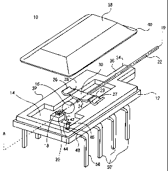
Figure 1 shows one embodiment of an optoelectronic assembly 10 with
frame 32 and flexure 24. Assembly 10 also includes a substrate 12 with
positioning floor 14, which may be substantially planar and the substrate 12
comprises an electronically isolating region with a low coefficient of thermal
expansion. In one embodiment, a raised platform is created on positioning
floor
14.
In one embodiment, the package comprises a substrate having a
positioning floor which provides a mounting surface and the package bottom
wall. In one embodiment, the substrate and its positioning floor are
substantially planar. In one embodiment, one or more raised platforms are also
provided on the mounting surface. The raised platforms may be submounts
made of a high thermal conductivity material, such as, for example, copper
tungsten, Aluminum Nitride, Berillyum Oxide, Diamond, and Boron Nitride,
attached to the floor of the substrate. The raised platforms may be attached,
for
example, by soldering or brazing, or may even be part of the substrate
material
itself.
Optical elements, or components, are mounted on positioning floor 14
and platform 20. In one embodiment, a lens 16 is mounted on substrate 12, and
6
CA 02383949 2005-09-09
an edge emitting optoelectronic element 18, such as, for example, a laser
diode,
is mounted on platform 20. Other optical components may be used.
An optical element 22 is attached to on flexure 24, by, for example,
soldering, brazing or welding. The optical element 22 provides a path for the
beam of radiation 19. In one embodiment, flexure 24 comprises two legs 26 and
27, a body 30, and two spring regions 28 and 29 at the junction of legs 26 and
27
and body 30. In one embodiment, element 22 is a single mode optical fiber, but
it may be any element that requires optical alignment with other optical
elements.
A frame 32 may be attached to substrate 12. The ends of legs 26 and 27
are attached to frame 32. Flexure 24 and its attachment method will be
discussed in more detail below. In one embodiment, frame 32 has a protruding
arm 34 having a groove 36. Groove 36 permits the hermetic passage of the fiber
22 to the outside of the package.
A cap 38 is attached to frame 32, thereby creating an airtight seal. In one
embodiment, cap 38 has a top hat shape and a peripheral lip 40 that can be
hermetically sealed to the outside portion of frame 32 and on top of groove 36
and fiber 22. The hermetic seal may be created by a process such as seam
welding, soldering or adhesive bonding.
In one embodiment, wire bond 42 connects active optical element 18 to
electrically conductive pattern 44 which is on the top side of positioning
floor
14. Filled conductive via 46 hermetically connects pattern 44 to electrically
conductive pattern 48 on the bottom side of positioning floor 14. Pins 50 on
the
bottom side of positioning floor 14 are also provided for connections to
electronic component inside the package through other vias (not shown). The
combination of patterns 48 and 44 and filled via 46 provide an efficient and
low-
parasitic mechanism for hermetically distributing electrical signals from
optoelectronic elements inside the hermetic enclosure to pins 50 at the
periphery
7
W~ ~l/1858~ CA 02383949 2002-03-04 pCT/US00/24666
of package 10. Alternatively, signals can be distributed to ball grid array
underneath the package for surface mounting.
Figures 2A-C, 3A-C, 4A and 4B illustrate a flexure alignment device and
alignment method. In one embodiment, flexure 24 comprises a body 30 and two
legs 26 and 27. Two spring regions 28 and 29 connect legs 26 and 27 to body
30.
The extremities of legs 26 and 27 rest on frame 32. In an alternative design,
the
extremities of the legs rest directly onto substrate 12. Body 30 holds an
optical
element 22. In one embodiment, the optical element 22 comprises an optical
fiber. In one embodiment, flexure 24 is preferably made from a flat stamped or
etched piece of spring steel. Spring regions 28 and 29 can be created by
chemically removing half of the metal thickness. Flexure 24, which is
substantially flat, is then subsequently formed in a press to shape legs 26
and 27
and spring regions 28 and 29, then annealed at high temperature to confer
spring properties to the material. In an alternative embodiment, the material
already has spring properties so no annealing is necessary. In one embodiment,
flexure 24 is about 170 microns thick, and spring regions 28 and 29 are
approximately 85 microns thick. It will be clear from the following how legs
26
and 27, body 30 and spring regions 28 and 29 are designed to allow for precise
three-dimensional alignment of optical element 22.
The process begins by first attaching optical element 22 to body 30 of
flexure 24 by a process such as, for instance, soldering or adhesive bonding.
Flexure 24 and its attached optical element are then picked and dropped in
rough alignment on optical assembly 10 as shown in Figure 2A. At this point,
flexure 24 simply rests on frame 32 (or on substrate 12, in a ring-less
embodiment), with no further attachment method. At least one first optical
element 16 is already attached on optical assembly 10 and defines an optical
axis
OA, with respect to which optical element 22 and its optical axis BC will be
aligned using flexure 24. In one embodiment, a laser diode 18 and a lens 16
are
8
CA 02383949 2005-09-09
attached on the optical assembly before flexure 24 is aligned. In one
embodiment,
flexure 24 is designed such that optical axis BC is higher than optical axis
OA, as
shown in the side view of assembly 10 on Figure 2B. In one embodiment, BC is
about 100 to 200 microns higher than OA when no pressure is applied on flexure
24. The top view of the assembly in Figure 2C shows that the axis OA and BC
may also be offset from each other in the horizontal plane alignment of
flexure 24.
Removable alignment tool 52 is used to apply pressure to the top of body 30.
Tool 52 also features pins 55 and 54 with conical ends 56 and 57 which fit
into
matching gripping holes 58 and 59 on body 30. It should be clear that the
shape of
the alignment tool in Figure 3A and 4B is just given as an example. Other
tools
that provide the ability to temporarily clamp onto the flexure and apply
pressure on
body 30 can be designed by one skilled in the art. For example, matching sets
of
grooves in the flexure and tool can replace the pin and hole interlocking
design. A
vacuum tool can also be used.
During the fine alignment step, tool 52 is lowered onto body 30. Conical
tips 56 and 57 are tightly fitted in holes 58 and 59. The tool applies
pressure on
body 30, causing spring regions 28 and 29 to bend under the pressure. This, in
turn, causes legs 26 and 27 to spread apart and axis BC to lower into
alignment to
axis OA, as shown on Figure 3B. Tool 52 is also moved in a plane parallel to
the
plane of mounting floor 14, dragging flexure 24 and legs 26 along with it
until
horizontal and longitudinal alignment of axis OA and BC is obtained, as can be
seen in the top view of Figure 3C. In one embodiment, alignment is monitored
by
measuring coupled power at the output of the fiber while laser 18 is powered
up
and flexure 24 undergoes fine alignment. Once desired alignment is obtained,
the
leg extremities are attached to the ring frame 32 or substrate 12. One
attachment
process is laser microwelding through laser beam 62, which creates welding
spots
60 and 61. Welding spots permanently attach metallic legs 26 to metallic ring
frame 32. Other attachment processes may also be used, such as UV curable
adhesives, epoxies, or soldering. After final attachment of the legs is
complete,
9
CA 02383949 2005-09-09
tool 52 is raised from the assembly, leaving the aligned assembly shown in
Figures
3B and 3C.
Most attachment processes induce minute, undesirable shift of drift during
the attachment operation. In the case of adhesives, shift is typically caused
by the
shrinkage of the adhesive; in the case of soldering, shift is caused by the
change of
solder volume during the solidification phase and by the expansion and
contraction
of parts during the temperature cycle; in laser welding, a post-weld shift is
usually
observed.
Figure 4A shows one flexure embodiment that reduces, or even minimizes,
the effect of such sifts and allows greater alignment precision and
reproducibility.
Flexure 70 of Figure 4A comprises two pairs of legs, a front pair of legs 26
and 27
and a rear pair of legs 74 and 75. The front pair of legs are located close to
the
optical element 16 shown in Figure 4B. The first optical element 27, which is
attached to the front portion of the flexure, is aligned with the second
optical
element 16 and is aligned using tool 52 and gripping holes 58 and 59 and
following
the previously described method. Front legs 26 and 27 are permanently attached
to
frame 32 as previously described using for example laser welding spots 60 and
61.
Post-attachment shift of the flexure is corrected in a second alignment step
by using
tool 52 and rear gripping holes 76 and 77 located in proximity of the rear
pair of
legs 74 and 75. The residual flexibility of flexure 70 allows a small
positioning
correction of tip 80 of optical element 22 by moving fear of flexure 70 with
tool 52.
After second alignment, rear legs are attached to frame 32 by laser welding
spots
78 and 79. Alignment tool 52 is then lifted from assembly. As discussed in
more
detail below, there are other ways to accommodate the welding process.
W~ 01/18580 CA 02383949 2002-03-04 pCT~S00/24666
Alternative Flexure Embodiments
Figure 5 illustrates an alternate embodiment of a flexure in Tigure 4A.
Referring to Figure 5, the flexure includes a body 86 and two pairs of legs,
in
which the spring portions 82 for connecting the two front legs have been
reduced. In Figure 5, body spring portions 82 coupling their associated front
legs 81 to the body 86 are smaller in total area than the spring portions 83
and 84
coupling the back legs 85 to body 86. This provides and additional freedom of
movement to body 86 after the front legs have been connected (e.g., welded).
This additional freedom of movement may be used to align an optical fiber (or
other component) coupled to the flexure after welding the front set of legs,
yet
before welding the back set of legs, such as is described above. This freedom
is
achieved by removing portions 89 of the flexure. This removal may occur after
legs 81 have been attached in the package.
Figure 6 is an alternative embodiment of the flexure. Referring to Figure
9, the flexure includes a body 96 and two pairs of legs, where the spring
portions
90 and 91 connecting the two front feet to the flexure body are reduced from
that
embodiment shown in Figure 4A. However, the shape of portions 93 and 94
gives a larger mechanical path between body 86 and the front feet and thus
greater mechanical flexibility.
Figure 7 illustrates an alternative embodiment of the flexure in Figure 4A
in which each of the feet (or some portion of the total number of feet) have a
pair
of holes between which a spot weld is made using a laser pulse to connect the
flexure to the substrate. Referring to Figure 7, one of the back legs is shown
having holes 101 and 102. At location 103 between holes 101 and 102, a spot
weld is made to secure the foot of the flexure to the substrate. Similarly,
holes
104 and 105 are shown with a spot weld location 106 between the two. Note that
the flexure in Figure 7 also includes a groove 115 for placement of the fiber.
11
CA 02383949 2002-03-04
WO 01/18580 PCT/US00/24666
Figure 8 illustrates an alternative embodiment to the flexure shown in
Figure 7. Referring to Figure 8, the flexure includes holes 1105 that are used
as
the locations for spot welding or other connection to the substrate. Similar
to
Figure 7, Figure 8 has spring portions 1109 that allow the body of the flexure
to
move up and down (i.e., move towards and away from the substrate). The
flexure also includes extraction, or removal, regions 1103 and 1104 that are
removed after the front feet of the flexure have been attached, yet prior to
the
back feet being welded. This is advantageous in that once removal regions 1103
and 1104 are removed, the body of the flexure may pivot about neck region 1101
with the fiber being moved in area 1102 in order to obtain better alignment of
the optical fiber (or component) coupled to the flexure. Thus, the body of the
flexure has portions which are joined at neck region 1101 which is much
smaller
in size that the portions its connecting (when viewed from a top view).
In one embodiment, when fabricating the optoelectronic assembly and
connecting the flexure to the substrate, the fabrication process includes a
series
of steps which begin with mounting the front feet to the substrate, then
removing removal regions 1103 and 1104. After removing removal regions 1103
and 104, the fiber (which is already coupled to groove region 1110) or other
component is aligned by moving the flexure body so that it pivots at neck
region
1101 and is free to move with respect to area 1102. Once alignment has been
achieved, the rear feet of the flexure are connected to the substrate.
Figure 9 illustrates a variation of the flexure embodiment in Figure 8.
Referring to Figure 9, the welding area to connect the flexure to the
substrate is
in the form of slots 1215 instead of holes 1105. The slots provide the benefit
of a
longer surface area for connection. For example, after the flexure has been
located onto the substrate and is pressed toward the substrate in order to
obtain
optical alignment of the optical components, the legs spread out. Because the
legs are spread farther apart, there is a greater likelihood that a portion of
the
12
CA 02383949 2002-03-04
WO 01/18580 PCT/LJS00/24666
slot (because of its length) will remain in contact with the substrate as
opposed
to having a circular hole as the cor nection point. When the feet only have
use of
a circular hole as a contact point, it is possible that after the flexure has
been
pressed towards the substrate, the hole may not be in direct contact with the
substrate any longer, which makes a welding process more difficult.
Figure 10 illustrates an alternative embodiment to the flexure in Figure 8.
Referring to Figure 10, the flexure includes removal regions 1301 and 1302
which
are removed after the front feet are attached to the substrate and prior to
the
connection of the back feet to facilitate alignment of the fiber coupled to
the
flexure body. Note that the optical component (e.g., fiber) coupled to the
flexure
body is mounted (e.g., soldered, glued, etc.) on the underside portion of the
flexure facing the substrate.
Figure 11 illustrates an alternative embodiment of the flexure in which
two regions of the flexure on each of the front two legs are removed after the
flexure has been connected to the substrate to facilitate movement of the
flexure
prior to securing the back legs. Referring to Figure 11, sections
1401,1402,1403
and 1404 are removed after the front legs have been secured to the substrate
so
that a region, such as region 1405, connects one of the feet to the flexure
body.
This removal gives us the flexures similar to the that shown in Figures 8 and
9.
The flexure also includes slots on the feet that provide more flexibility.
Note that
the optical component (e.g., fiber) coupled to the flexure body is mounted
(e.g.,
soldered, glued, etc.) on the underside portion of the flexure facing the
substrate.
Figure 12 illustrates still another embodiment of a flexure in which
regions 1501 and 1502 are removed after securing the front feet of the flexure
which are coupled to regions 1501 and 1502, thereby allowing neck region 1503
to act as a pivot when aligning the fiber. The flexure also includes side
areas
1505 and 1506 that add rigidity to the body. Note that the optical component
13
CA 02383949 2002-03-04
WO 01/18580 PCT/US00/24666
(e.g., fiber) coupled to the flexure body is mounted (e.g., soldered, glued,
etc.) on
the underscale portion of the flexure facing the substrate.
Figure 13 illustrates another alternate embodiment of the flexure in which
regions 1601 and 1602 coupling, in part, the front feet to the flexure body
are
removed after securing the front feet to the substrate, allowing the rear
portions
of the flexure to move around neck region 1603 when aligning the fiber. Each
of
the feet have a pair of slots. Securing the feet of the flexure embodiment is
performed by welding in an area of the flexure, such as 1606 between slots
1605
and 1604 on each of the feet. Rigid regions 1607 add support to the flexure.
Figure 14 illustrates an alternative embodiment of the flexure. The
flexure includes side areas, rigidizer 1706, on the body for added stiffness
and
rigidity. Again, the flexure of Figure 14 includes removable areas 1701 and a
neck region 1703 to allow aligning of the fiber which sits in and is coupled
to
groove 1705 during the fabrication process.
Figure 15 illustrates another embodiment of a flexure. The significance of
the difference in the neck region of this flexure and the one in Figure 14 is
that
there are different distances between pivot joint and fiber tip.
To facilitate the assembly process, in one embodiment, the flexures
include a tail area for centering the fiber. Figures 16,17, 18 and 19
illustrate
alternative embodiments of the flexure having fins. Figures 16 and 18
illustrate
such a centering area in the form of fins on either side of a groove that
supports
a fiber. Referring to Figure 16, fins 1901 and 1902 are used to center the
fiber.
Also, the flexure in Figure 18 has weld strips, or weld / contact areas,1905
for
welding the flexure, as well as rigid regions. Similarly, referring to Figure
17,
fins 2001 and 2002 are used for centering the fiber.
The mechanical system described herein may be used for aligning other
precision parts having a similar alignment tolerances, such as magnetic
recording heads, MEMs, and medical equipment, etc.
14
CA 02383949 2002-03-04
WO 01/18580 PCT/US00/24666
Whereas many alterations and modifications of the present invention will
nc doubt become apparent to a person of ordinary skill in the art after having
read the foregoing description, it is to be understood that any particular
embodiment shown and described by way of illustration is in no way intended
to be considered limiting. Therefore, references to details of various
embodiments are not intended to limit the scope of the claims which in
themselves recite only those features regarded as essential to the invention.