Note : Les descriptions sont présentées dans la langue officielle dans laquelle elles ont été soumises.
WO 01/50744 CA 02384452 2002-03-05 PCT/USO1/00159
HDTV RECEIVER HAVING FAST DIGITAL IF AGC AND ANALOG RF AGC
BACKGROUND OF THE INVENTION
This invention relates generally to digital data receivers and specifically to
a novel
AGC (automatic gain control) system for HDTV (high definition television)
receivers.
United States Patent No. 5,565,932, entitled AGC SYSTEM WITH PILOT
USING DIGITAL DATA REFERENCE, issued October 15, 1996 to Zenith Electronics
Corporation, describes a digital television signal that is formatted in a
plurality of repetitive data
segments, with each data segment consisting of a fixed number of multilevel
symbols occurring
at a constant symbol rate of 10.76 megasymbols per second. In a receiver, the
multilevel
symbols are converted to corresponding digital values and the pilot, that is
represented by a DC
offset in the signal, is removed. The symbols are sampled, accumulated and
divided to derive an
average symbol value. This value is compared to a reference average symbol
value to develop
an AGC voltage for controlling the IF gain (and thereby the RF gain) of the
receiver.
Difficulties arise in the AGC processing of rapidly changing RF signals that
reach
the receiving antenna. The effects of phase, delay and signal strength of
dynamically ghosted
signals, or of atmospheric conditions, can result in rapid changes in the
total received RF signal
level. A fast-acting AGC system in a receiver will tend to minimize such
changes, resulting in
less clipping in the analog processing circuits, particularly the IF circuits.
If a signal is severely
clipped, digital data will be lost and the receiver error correction circuitry
will begin to fail. A
=1) iast receiver AGC will also reduce the speed requirements on the receiver
equalizer, a task of
~~ hich is to cancel the amplitude variations in the received signal.
1
CA 02384452 2007-02-22
Fast AGC systems are also particularly effective
against zero or short delay dynamic ghosts. Such ghosts
often occur in a home environment when people walk in
front of an indoor antenna. In these instances, the
delays are very short between the received direct and
ghosted signals and the effect is much like a fast
varying attenuation of a received signal. Because the
tuner is designed to accommodate a large range of input
signals, distortion is low, even in the presence of a
dynamically changing RF input signal. because of this,
the IF AGC can be called upon to immediately track and
compensate for fast moving RF signal variations and the
tuner AGC can be designed to adjust its gain at a much
lower rate. In the implementation of this invention, the
fast AGC is applied to the IF whenever called for and is
not dependent upon the shower, non-linear tuner AGC and
the tuner AGC delay point.
The present invention provides an AGC system for a
digital data receiver having a tuner that includes RF
circuitry and IF circuitry and which receives a digital
signal including a pilot and a plurality o multilevel
data symbols occurring at a constant symbol rate
comprising means for converting said received data
symbols to digital values; means for removing the effects
of said pilot on said digital values; digital AGC means
including an accumulator for determining an error value;
means for controlling the gain of said IF circuitry based
upon said error value; and analog AGC means including
capacitance means for controlling the gain of said RF
circuitry.
The present invention also provides an AGC system
2
CA 02384452 2007-02-22
for a digital data receiver having a tuner that includes
RF circuitry and IF circuitry and which receives a
digital signal including a pilot and a plurality of
multilevel data symbols occurring at a constant symbol
rate comprising means for converting said received data
symbols to digital values; means for removing the effects
of said pilot on said digital values; digital AGC means
including a continuously operated accumulator for
determining an error value; the most significant bits of
the value in said accumulator comprising said error
value; a combiner supplied with said digital values; a
reference digital value.coupled to said combiner, the
output of said combiner connected to said accumulator;
means for controlling the gain of said IF circuitry based
upon said error value; and analog AGC means including
capacitance means for controlling the gain of said RF
circuitry.
With the invention, the IFAGC performance is
optimized for speed, by employing a large capacity,
continuously operated, with the most significant bits of
the accumulated value being the generated AGC error
correction signal. The use of the accumulator retains
more resolution from the sampled data signal and the
system can therefore operate in a controlled manner at a
higher AGC speed. Among the benefits are: control is
more precise in that errors associated with analog
circuit leakage currents are eliminated; the AGC delay
point is digitally stored, eliminating the need for a
potentiometer, and digital averaging techniques can be
applied to the detected amplitude of the recovered
signal.
3
CA 02384452 2007-02-22
BRIEF DESCRIPTION OF THE DRAWINGS
These and other objects and advantages of the
invention will be apparent upon reading the following
description in conjunction with the drawings in which:
FIG 1 is a simplified block diagram of a prior art
digital television receiver; and
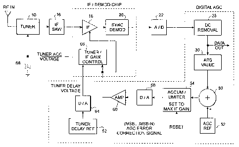
FIG 2 is a simplified diagram of a digital
television receiver of the invention that includes a
digital IF AGC circuit and an analog RF AGC circuit.
DETAILED DESCRIPTION OF THE INVENTION
Referring to FIG 1, a received RF signal is
converted to an IF signal by a.tuner 10. The IF output
of tuner 10 is supplied to a SAW (surface acoustic wave)
filter 16 and thence to an IF amplifier 18. The output
of IF amplifier 18 is supplied to a synchronous
demodulator 20 that in turn feeds an A/D (analog to
digital) converter 22 in which the amplitudes of the
received symbols are converted to corresponding digital
values. A/D converter 22 supplies a data recovery
circuit 24 where the data symbols are recovered, a symbol
clock recovery circuit 26, where timing signals are
developed based upon synchronization information in the
received signal; and a DC removal circuit 28 where the DC
is removed. The DC removal circuit may also comprise a
linear filter such as a post comb filter. The DC
represents the pilot and uniformly affects all symbol
values in the form of an offset. The output of the DC
removal circuit 28 is supplied to an absolute value
circuit 30, which provides an output representing the
magnitude of the symbols. Absolute value circuit 30
rectifies the values of the received symbols which may
3a
WO 01/50744 CA 02384452 2002-03-05 PCT/USO1/00159
assume negative as well as positive levels. The absolute value circuit 30
supplies its output to a
sampler 32, which is controlled by a divide-by-four counter 34.
Symbol clock recovery circuit 26 provides a timing signal to. A/D converter
22,
divide-by-four counter 34 and an accumulator and divider circuit 36, which is
also supplied with
the output of sampler 32. This timing signal preferably comprises a clock
signal at the symbol
rate of 10.76 megasymbols per second. The output of the accumulator and
divider circuit 36
comprises the average value of the sampled data symbols over a predetermined
time interval and
is supplied to the positive input terminal of a combiner 38. The negative
input terminal of
combiner 38 is supplied with a reference AGC offset 40 representing the known
average value of
the symbols. This value is based upon the symbols occurring randomly and a
knowledge of the
symbol levels as determined from the VSB (vestigial sideband) mode of the
signal. Subtraction
of the AGC offset from the determined average symbol level represents an AGC
signal that is
supplied to an AGC logic block 42, which distributes the AGC signal between IF
18 and tuner
10.
Initially, both the tuner and IF AGC operate at maximum gain to assist in
carrier
acquisition because of the low level pilot in the signal. The sampler circuit
32 samples every nth
symbol and supplies that value to accumulator and divider circuit 36, which
accumulates the
symbol values for a fixed number of sampled signals y and divides that amount
by y to yield a
derived average value of a received data symbol. The determined average symbol
value is
compared with the AGC offset value and the AGC is developed for reducing the
gain of the IF
from maximum based upon the comparison. The tuner AGC is developed and applied
in
accordance with an algorithm that governs the desired relationship between the
tuner and IF
4
WO 01/50744 CA 02384452 2002-03-05 PCT/US01/00159
gains. It will be appreciated that the various elements of the receiver are
under microprocessor
control, which circuitry is omitted for the sake of simplicity.
In FIG 2, a digital television receiver including the AGC system of the
invention
is shown. In contrast with the prior art arrangement of FIG 1, the invention
uses a digital IF
AGC in conjunction with an analog RF AGC, as well as an accumulator that is
operated on a
continuous basis as opposed to the prior art sampled accumulator, which was
reset at the start of
each accumulation period. It will, of course, be understood that upon
occurrence of an ON/OFF
or channel change event, the accumulator of the invention (as well as that of
the prior art circuit)
is reset to maximum to force maximum tuner and IF gain. Also, the practice of
gain controlling
the tuner using a tuner delay input along with the IF AGC voltage is common in
receiver AGC
design.
The DC removal circuit 25 and absolute value circuit 30 of FIG 1 are
replicated in
FIG 2, with the output of absolute value circuit 30 being applied to the
negative input of a
combiner 50. A reference sienal is applied to the positive input of combiner
50, the algebraically
1; derived output of which is applied to a relatively large
accumulator/limiter 54. This provides for
a proper negative feedback condition for the AGC. The accumulator size is
predetermined so as
to preclude overflow under normal signal conditions. The output of
accumulator/limiter 54,
consisting of the most significant bits of its contents (an example being the
use of bits 20-9), is
applied to a D/A (digital to analog) converter 58_ A balance between the size
of
1_0 accumulator/limiter 54, the number of bits supplied to D/A converter 58
and the gain of an
interface amplifier 60 determines the speed and steady state accuracy of the
AGC system. The
output of D/A converter 58 is supplied, via interface amplifier 60, to IF
amplifier 18 and to a
5
WO 01/50744 CA 02384452 2002-03-05 PCT/USOl/00159
tuner/iF gain control block 66. The RF AGC is developed using a tuner AGC
delay reference 62
to delay the onset of the RF gain reduction until most or all of the IF gain
reduction has been
attained in accordance with common practice. The tuner delay is a constant
that is determined at
the factory in accordance with well-known tuner operating principles for
optimizing the
receiver's signaUdistortion characteristics. The tuner delay reference 62
signal is applied through
a D/A converter 64 to the tuner/IF gain control block 66, the output of which
supplies a filter
capacitor 68. The RF AGC voltage is taken from filter capacitor 68 and
supplied to tuner 10.
Thus, a digitally-derived AGC is applied to the IF, whereas the RF AGC is
derived on an analog
basis.
Upon the occurrence of a channel change or an ON/OFF event,
accumulator/limiter 54 is set to a value that forces maximum IF gain to insure
that the IF, and
thus the tuner gain, is large enough for proper startup synchronization. After
this the
accumulator is operated continuously. The absolute value of each incoming data
symbol level is
combined with the preset AGC reference symbol value in combiner 50 and the
algebraic result
l; supplied to accumulator/limiter 54 which counts or accumulates the total.
The error signal
comprises the most significant bits of the total number in accumulator/Iimiter
54 and is converted
to the analog voltage required to adjust the gain of IF amplifier 18 and
tuner/IF gain control
block 66. As the incoming data symbol level from absolute value circuit 30
approaches the
symbol level represented by AGC reference 52, the input to accumulator/limiter
54 becomes
~C smaller with the error signal falling to zero, stabilizing the average
symbol level at the output of
the absolute value circuit 30 to the AGC reference symbol level. With the
output of the absolute
6
WO 01/50744 CA 02384452 2002-03-05 PCT/US01/00159
value circuit 30 being stabilized, the data output signal, which is the input
of DC removal circuit
25, is also stabilized.
The RF AGC is developed conventionally, with the voltage on capacitor 68
approaching a stable value after the digital IF AGC has first accommodated any
fast changes in
RF signal level. A further adjustment in IF AGC follows in response to any
changes in tuner
AGC stabilization. Taken together, the AGC system of the invention performs as
well as the
prior art system with the added advantaae that overall receiver performance in
the presence of
fast changing RF signal strength is improved.
What has been described is a novel AGC system for a digital data receiver. It
is
recoenized that numerous changes to the described embodiment of the invention
will be apparent
without departing from its true spirit and scope. The invention is to be
limited only as defined in
the claims.
7