Note : Les descriptions sont présentées dans la langue officielle dans laquelle elles ont été soumises.
CA 02384818 2002-O1-23
WO 01/19048 PCT/US00/40355
-1-
Description
DUAL AUTOMATIC GAIN CONTROL IN A QAM DEMODULATOR
TECHNICAL FIELD
The present invention relates to a quadrature
amplitude modulation (QAM) type demodulator for
demodulating signals modulated in accordance with the QAM
scheme.
BACKGROUND ART
Quadrature amplitude modulation (QAM) is an
intermediate frequency (IF) modulation scheme in which a
QAM signal is produced by amplitude modulating two
baseband signals, generated independently of each other,
with two quadrature carriers, respectively, and adding
the resulting signals. The QAM modulation is used to
modulate a digital information into a convenient
frequency band. This may be to match the spectral band
occupied by a signal to the passband of a transmission
line, to allow frequency division multiplexing of
signals, or to enable signals to be radiated by smaller
antennas. QAM has been adopted by the Digital Video
Broadcasting (DVB) and Digital Audio Visual Council
(DAVIC) and the Multimedia Cable Network System (MCNS)
standardization bodies for the transmission of digital TV
signals over Coaxial, Hybrid Fiber Coaxial (HFC), and
Microwave Multi-port Distribution Wireless Systems (MMDS)
TV networks.
The QAM modulation scheme exists with a
variable number of levels (4, 16, 32, 64, 128, 256, 512,
1024 ) which provide 2, 4, 5, 6, 7, 8, 9, and 10
Mbit/s/MHz. This offers up to about 42 Mbit/s (QAM-256)
over an American 6 MHz CATV channel, and 56 Mbit/s over
an 8 MHz European CATV channel. This represents the
equivalent of 10 PAL or SECAM TV channels transmitted
CA 02384818 2002-O1-23
WO 01/19048 PCT/iJS00/40355
-2-
over the equivalent bandwidth of a single analog TV
program, and approximately 2 to 3 High Definition
Television (HDTV) programs. Audio and video streams are
digitally encoded and mapped into MPEG2 transport stream
packets, consisting of 188 bytes.
The bit stream is decomposed into n bits
packets. Each packet is mapped into a QAM symbol
represented by two components I and Q, (e. g., n=4 bits
are mapped into one 16-QAM symbol, n=8 bits are mapped
into one 256-QAM symbol). The I and Q components are
filtered and modulated using a sine and a cosine wave
(carrier) leading to a unique Radio Frequency (RF)
spectrum. The I and Q components are usually represented
as a constellation which represents the possible discrete
values taken over in-phase and quadrature coordinates.
The transmitted signal s(t) is given by:
s ( t) =Icos (2nfot) - Qsin (2nfot) ,
where fo is the center frequency of the RF signal. I and
Q components are usually filtered waveforms using raised
cosine filtering at the transmitter and the receiver.
Thus, the resulting RF spectrum is centered around fo and
has a bandwidth of R(1+cc), where R is the symbol
transmission rate and cx is the roll-off factor of the
raised cosine filter. The symbol transmission rate is
1/nt" of the transmission bit rate, since n bits are
mapped to one QAM symbol per time unit 1/R.
In order to recover the baseband signals from
the modulated carrier, a demodulator is used at the
receiving end of the transmission line. The receiver
must control the gain of the input amplifier that
receives the signal, recover the symbol frequency of the
signal, and recover the carrier frequency of the RF
signal. After these main functions, a point is received
in the I/Q constellation which is the sum of the
w... ~ ~,u n~rICES T1-IOMAS SCHNECK . 408 297 9748, 11 ! ~ I ! u~ 4 : a7CrM,
J~~xvti~ ~. u:,.. , . . ..
28-11-2001 CA 02384818 2002-O1-23 US0040355
-3 -
transmitted QAM syiobol and noise that was added over the
transmission. The receiver then carries out a threshold
decision based on lines situated at half the distance
between QaAM symbols in order to decide on the most
~5 probable sent GRM symbol. From this symbol, the bits are
unmapped using the same mapping as in the modulator.
Usually, the bits~then go through a forward error decoder
which corrects possible erroneous decisions on the actual
transmitted QRM symbol. ~ The~forward error decoder
usually contains a de-interleaves whose role is to spread
out erroxs that could have happened in bursts and would
have otherwise have be~n more difficult to correct.
Generally, in transmitting a modulated signal,
the received signal at the demodulator has been amplified
by a suitable amplification factor in order to compensate
for attenuation in the received signal due to a
transmission path or other factors. Tt is therefore
necessary to control the amplification of the signal to
control the received level of the signal. In order to
2(~ control'the level of the signal, often an automatic gain
control (AGC) circuit, which controls the gain of the
amplifier supplying the demodulator, is employed. For
example, tl.S. Patent No. .5,72.9,173 to Sato discloses a
QAM demodulator for receivinq a QAM signal having a
suppressed pilot signal. (Pilots exist in VSB
modulations, but in QAM modulation, no pilot is
necessary. arid in general they are not used.) The
demodulator includes an amplification factor controller
in which the control of the amplification factor is
performed separately from the control of the sampling
timing for a received signal. Also, U.S. Patent No.
5,761,251 to Wander discloses a circuit arrangement for '
achieving both DC offset correction and automatic gain
control.for QiAM modulation. An article by M. Kayo et al.
entitled "High Speed Modem Using Digital Signal
Processor" (International Conference on Communications,
Emvfar.AMENDED SHEET
28-11-2001 DOES THOMAS~ SOHNE~K 408 297 9748; 11 !27!01 4: azrM;~gttaac_~o.~~;
raga . ~. ."
CA 02384818 2002-O1-23 US0040355
US, NeW~York, IEEE, June 1981, pages 19.7.1-14.7.5)
discloses a digital modem having 3 digital signal
processor with high speed multiplier. Also, U.S. Patent
No. 4,355,402 disclQSes circuitry for detecting and
correcting false equilibrium conditions generated in data
modems by sudden changes in gain of an assaciated
transmission system. In many of the prior art designs,
the automatic gain control tAGC) circuit is based
uniquely on the SAM signal but with feedback to -
1
x_
if
Emofa.AMENDED SHEET
CA 02384818 2002-O1-23
WO 01/19048 PCT/US00/40355
_q_
other analog circuits. This can cause the problem of
saturation of the analog-to-digital converter circuit
used at the input of the demodulator. Alternatively,
other prior art designs use an AGC circuit that is based
uniquely on the full input signal. However, this
requires that the input signal has to have been perfectly
filtered from adjacent channels prior to being input to
the demodulator.
It is the object of the present invention to
provide a QAM demodulator that provides gain control both
prior to the demodulator, in order to prevent signal
distortion caused by amplifier non-linearity and A/D
saturation, and within the demodulator, to adapt the
level of the QAM signal to the correct level with digital
gain.
It is a further object of the invention to
provide a QAM demodulator wherein the gain control is
independent with respect to adjacent channels, and is
therefore independent with respect to the symbol rate of
the input signal.
It is a further object of the invention to
provide a QAM demodulator with gain control that does not
saturate the A/D converter.
SUMMARY OF THE INVENTION
The above objects have been achieved by a QAM
demodulator having a first automatic gain control circuit
which outputs a first signal that is a function of the
received signal, the first signal being used to control
the gain of an amplifier which supplies the input of an
A/D converter; and a second automatic gain control
circuit which outputs a second signal derived from the
QAM signal after filtering. The second signal controls
the gain of a digital multiplier which produces a signal
which feeds into an equalizer by way of a receive filter.
The dual automatic gain control circuits, situated before
CA 02384818 2002-O1-23
WO 01/19048 PCT/LJS00/40355
-5-
and after the receive filters, allow for better
resistance to non-linearities caused by signals in
adjacent channels.
The first automatic gain control (AGC) circuit
controls the entire power of the signal that enters the
A/D converter, comprising the desired spectrum but also
adjacent channels that have not been completely filtered
out before entering the demodulator. This allows the
maximum range of the A/D converter to be used and ensures
that no analog saturation can occur due to the AGC
feedback. The second AGC circuit is situated after the
receive filter and therefore only has to take into
account the signal itself. The second AGC circuit adapts
the internal amplification level to the exact decision
threshold of QAM signal levels and compensate for the
attenuation caused by the presence of adjacent channels
in the first AGC circuit.
BRIEF DESCRIPTION OF THE DRAWINGS
Fig. 1 is a block diagram of a Network
Interface Unit in which the demodulator of the present
invention may be used.
Fig. 2 is a block diagram of the demodulator of
the present invention.
Fig. 3 is a block diagram of the first AGC unit
of the demodulator shown in Fig. 2.
Fig. 4 is a block diagram of the second AGC
unit of the demodulator shown in Fig. 2.
Fig. 5 is a block diagram of a section of the
demodulator shown in Fig. 2.
Fig. 6 is a block diagram of the Direct Digital
Synthesizer of the demodulator shown in Fig. 2.
Fig. 7 is a block diagram of the digital timing
recovery circuit of the demodulator shown in Fig. 2.
Fig. 8 is a block diagram of a generally known
interpolation model.
CA 02384818 2002-O1-23
WO 01/19048 PCT/US00/40355
-6-
Fig. 9 is a block diagram of an interpolation
model used in the digital timing recovery circuit of Fig.
7.
Fig. l0 is a block diagram of a phase noise and
additive noise estimator used in the symbol detection
circuit of the demodulator of Fig. 2.
Fig. 11 is a block diagram of the Dual Bit
Error Rate estimator used in the demodulator of Fig. 2.
BEST MODE FOR CARRYING OUT THE INVENTION
With reference to Fig. 1, the QAM demodulator
99 of the present invention would typically be used as
part of a Network Interface Unit 92. The Network
Interface Unit 92 is defined as the interface block
between a signal 95 received from a Cable Network and the
input signal 93 of a demultiplexer. The signal 95 from
the cable network is input into a tuner 96. The tuner
accepts frequencies in the range of 47 MHz to 862 MHz at
its input and down converts the selected frequency to an
intermediate frequency (IF). This IF frequency depends
on the channel bandwidth as related to the geographic
location. For example, NTSC, USA and JAPAN have a 6 MHz
channel with IF around 44 MHz, while PAL/SECAM and EUROPE
have an 8 MHz channel with IF around 36 MHz. The output
of the tuner is input to a surface acoustic wave (SAW)
filter 97, the IF frequency being equal to the SAW filter
center frequency. The output of the SAW filter 97 is
supplied to an amplifier 98, which is used to compensate
for the SAW filter attenuation, and then the output of
the amplifier 98 is supplied to the QAM demodulator 99.
The amplifier 98 can also have a variable gain controlled
by an Automatic Gain Control signal 94 of the QAM
demodulator 99. It is also possible for the QAM
demodulator 99 to be used in various other digital
transmission systems using QAM or QPSK demodulation, such
CA 02384818 2002-O1-23
WO 01/19048 PCT/US00/40355
as radio links, wireless local loops, or in-home
networks.
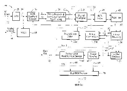
Referring to Fig. 2, the QAM demodulator 99 of
the present invention includes an analog-to-digital (A/D)
converter 25 which receives the IF input signal 12. The
A/D converter 25 samples the IF signal 12 and produces a
digital spectrum around the center frequency Fo of the IF
signal 12. The output signal 14 of the A/D converter 25
is supplied to a baseband conversion circuit that
includes a Direct Digital Synthesizer 30 in order to
convert the IF signal to a baseband signal. The output
signal 14 of the A/D converter 25 is also supplied to the
first Automatic Gain Control circuit (AGCl) 10 for
controlling the analog gain of the input signal 12 of the
A/D converter 25.
After the signal has been converted to a
baseband signal having signal components I (inphase) and
Q (quadrature), the baseband signal is supplied to a
timing recovery circuit 35 which is used to synchronize
the timing of the demodulator circuit to the symbols of
the incoming signals. The timing recovery circuit 35
uses a continuously variable interpolation filter for
sampling the input signal which allows the circuit to
recover a very large range of symbol rates, as will be
further explained below. The signal is then supplied to
a digital multiplier 210 which is part of a second
Automatic Gain Control (AGC2) circuit 20. Then, the
signal goes through a Receive Filter 40 and then to an
Equalizer 45. The AGC2 circuit 20 is a digital AGC
circuit and performs a fine adjustment of the signal
level at the equalizer 45 input. The digital AGC circuit
20 only takes into account the signal itself, since
adjacent channels have been filtered out by the receive
filter 40, and thus compensates digitally for the analog
AGC1 circuit 10 which may have reduced the input power
due to adjacent channels. The receive filter 40 is a
CA 02384818 2002-O1-23
WO 01/19048 PCT/US00/40355
_g_
squared root raised cosine type which supports roll-off
factors from 0.11 to 0.30, which accepts the timing
recovery circuit output signal and ensures an out-of-band
rejection higher than 43dB. This significant rejection
increases the back off margin of the Network Interface
Unit against adjacent channels. The equalizer 45
compensates for different impairments encountered on the
network, such as undesired amplitude-frequency or phase-
frequency response. Two equalizer structures can be
selected, Transversal or Decision feedback with
selectable central tap position.
The output signals of the equalizer 45 are
supplied to the carrier recovery circuit 50 to recover
the carrier signal. The carrier recovery circuit 50
allows the acquisition and tracking of a frequency offset
as high as 12 percent of the symbol rate. The frequency
offset recovered can be monitored through a I2C
interface. This information can be used to readjust the
tuner or the demodulator frequency in order to reduce the
filtering degradation of the signal, which helps to
improve the bit error rate. The output signal 52 of the
carrier recovery circuit 50 is supplied to a symbol
decision circuit 55 and is also supplied to a Power
Comparator Circuit 230 and Digital Loop Filter 220 within
the digital AGC2 circuit 20 to provide a gain control
signal 225 to the multiplier 210. Within the symbol
decision circuit 55, the signal is supplied to a symbol
threshold detector, then to a differential decoder, and
finally to a DVB or DAVIC de-mapper which produces the
recovered bit stream 57 sent to the Forward Error
Correction Circuit 60. The output 57 of the symbol
decision circuit is also supplied to the Power Comparator
Circuit 230.
The Forward Error Correction (FEC) circuit 60
first performs a frame synchronization 61 in which the
bit stream is decomposed into packets of 204 bytes at the
CA 02384818 2002-O1-23
WO 01/19048 PCT/US00/40355
-9
output. The packets are then supplied to a de-
interleaver and Reed-Solomon (RS) decoder 65, where the
packets are de-interleaved and then a correction is
performed by the RS decoder of a maximum of 8 errors
(bytes) per packet. The RS decoder also provides other
information regarding the uncorrected packets and the
position of the corrected bytes in the packet, if there
are any. Two depths can be selected for the interleaver:
12 (DVB/DAVIC) and 17. The depth 17 increases the
strength of the system against impulse noise, but assumes
that the signal has been interleaved with the same value
at the monitor. After RS decoding, the packets are de-
scrambled for energy dispersal removal. The data output
93 of the FEC circuit 60 is constituted of the MPEG2
Transport System (TS) packets and is the output of the
demodulator 99. Additionally, bit error rate signals 68,
69 are transmitted to a Dual Bit Error Rate Estimator
circuit 70 which estimate Low and High Bit Error Rates
based on error correction and frame pattern recognition
and produces a Bit Error Rate Signal 72.
As explained above, the dual automatic gain
control (AGC) circuits are situated before and after the
receive filters to control the received level of the
signal. The first AGC circuit 10 controls the analog
gain of the input signal of the A/D converter. With
reference to Fig. 3, the output signal 14 of the A/D
converter 25 is supplied to a power estimation circuit
110 of the AGCl 10 in order to estimate the signal level
of the received signal 14 and compare it to a
predetermined signal level. The power estimation circuit
110 includes a square module 130 for converting the
signal 14 into a square wave to be input into a
comparator 140. The comparator 140 compares the input
signal with a predetermined reference voltage, or
comparator threshold voltage, and produces an output
signal when the level of the input signal matches the
CA 02384818 2002-O1-23
WO 01/19048 PCT/US00/40355
-10-
level of the comparator threshold voltage. The
comparator threshold voltage, or reference voltage, can
be adapted by a modification circuit 120. The
modification circuit 120 monitors the presence of signals
from adjacent channels 125 and adapts the reference
voltage accordingly. Additionally, a detection of
saturation counter 115 detects whether there is any
saturation in the A/D converter and, if so, sends a
signal to the modification circuit 120 in order to adjust
the reference voltage in order to eliminate the
saturation. After the signal goes through the comparator
140, the output signal of the power estimator circuit 110
is supplied to a digital loop filter 150 which removes
the carrier-frequency components and harmonics from the
signal, but passes the original modulating frequencies of
the signal. The digital loop filter 150 receives a
configuration signal 152 which sets the amplifier maximum
gain configuration for limiting non-linearities. The
output signal 162 of the digital loop filter 150 is
converted to a Pulse Width Modulated (PWM) signal 160
which is supplied to an RC filter 170 which produces a
signal 167 that controls the analog gain of the amplifier
of the A/D converter. Another output of the digital loop
filter provides a signal 155 for monitoring the gain
value of the digital loop filter. Since the power
estimation is estimated by the digital loop control, the
PWM signal that controls the analog gain generates very
stable control.
The second AGC circuit 20 is situated after the
receive filter 40, therefore only having to take into
account the received power of the QAM signal itself, and
adapts the internal amplification level to the correct
level before threshold decision. The second AGC circuit
20 compensates for the attenuation of the first AGC
circuit 10, which is caused by the presence of adjacent
channels, and also adapts the signal level exactly to the
CA 02384818 2002-O1-23
WO 01/19048 PCT/US00/40355
-11
decision threshold levels of the QAM signal. With
reference to Fig. 4, the output signal 42 of the timing
recovery circuit is supplied to the digital multiplier
210 of the second AGC circuit 20. The digital multiplier
210 multiplies the signal, which is then supplied to the
receive filter 40, equalizer 45 and carrier recovery 50
circuits as explained above. The output of the carrier
recovery circuit 50 is fed back into a power comparator
circuit 230 of the second AGC circuit 20 which compares
the output signal 52 from the carrier recovery circuit
with a set of QAM values. A digital loop filter 220
filters out any error signals and provides a gain control
signal 225 to the digital multiplier 210. Additionally,
a signal 227 can be provided from the digital loop filter
in order to monitor the amount of gain.
With reference to Figs. 5 and 6, the
aforementioned Direct Digital Synthesizer (DDS) 30
digitally tunes the signal 14 from the A/D converter 25
to be within the bandwidth of the receive filter 40 even
in the case of a large frequency offset of the receiver
and provides more flexibility in the frequency values
used by the input signal. The Intermediate Frequency
(IF) to baseband signal conversion is accomplished by
using a combination of a first DDS 30 before the receive
filter 40 in order to digitally tune the signal within
the receive filter bandwidth, and a second DDS 545 within
the carrier recovery circuit 50 to fine tune the signal
phase after the timing recovery 35 and equalizer 45
circuits.
Referring to Fig. 6, after the IF signal 12
passes through the A/D converter 25, the output digital
signal 14 of the A/D converter is supplied to a
multiplier 304 that is part of DDSl 30. The multiplier
304 converts the digital signal 14 into two parallel
components, I (inphase) and Q (quadrature) which form a
QAM symbol. These signal components proceed through the
CA 02384818 2002-O1-23
WO 01/19048 PCT/US00/40355
-12
receive filter 40, equalizer 45 and carrier recovery 50
circuits, as explained above. Referring to Fig. 5, the
carrier recovery circuit 50 includes a frequency offset
detect 525 circuit and a phase offset detect 535 circuit
for recovering the carrier signals to be sent to the
digital AGC2 circuit 20 and the symbol detection circuit
55. The frequency offset recovered can be monitored
through an I2C interface and the information can be used
to readjust the tuner frequency in order to reduce the
filtering degradation on the signal and thus improve the
bit error rate. This information can also be sent as a
signal 527 to the DDSl circuit 30 in order to recover the
frequency with complete accuracy before the receive
filter 40. The phase detect circuit 535 sends a signal
537 to the DDS2 circuit 545. Employing a dual DDS
structure to control the down conversion of the IF signal
to a baseband signal is advantageous in that the long
loop frequency down-conversion is optimal for frequency
recovery since it is done before the receive filter 40 in
order to maintain the maximum signal energy before
equalization and carrier frequency estimation, while the
short loop carrier phase recovery is optimal for phase
tracking, especially in case of phase noise on the
signal.
Referring to Fig. 6, the carrier recovery
frequency feedback signal 527 is supplied to an adder
circuit 306 within the DDS1 circuit 30. The adder
circuit 306 adds the frequency feedback signal 527 to the
configured IF frequency 27 and the resulting signal is
supplied to a phase accumulation circuit 305 which
accumulates frequency elements determined by the
frequency feedback signal 527. The signal is supplied to
a constant table 303 containing sinusoidal values which
synthesizes the signal. The synthesized signal 316 is
supplied back into the multiplier 304. Referring back to
Fig. 5, the second DDS2 circuit 545 operates in the same
CA 02384818 2002-O1-23
WO 01/19048 PCT/US00/40355
-13
manner except that it synthesizes the output signal 537
of the phase detect circuit 535. The purely digital
carrier recovery eliminates the need for a voltage
controlled oscillator (VCO) to be used and provides a
better carrier recovery in terms of accuracy and the
residual phase noise of the signal.
With reference to Fig. 7, the timing recovery
circuit 35 uses a symbol rate continuously adaptive
interpolation filter 352 for resampling the input signal.
As opposed to prior art methods of interpolation which
use interpolation functions which are defined as function
of t/TS (time/sampling Interval), the method of
interpolation used in the timing recovery circuit 35 is
defined as a function of t/Ti (time/Interpolation
Interval). This allows the interpolation filtering to be
totally independent of the symbol rate in terms of
performance and complexity and provides a better
rejection of adjacent channels since the interpolator
rejects most of the signal outside the bandwidth of the
received channel.
The objective of interpolation in modem
applications is to process digital samples x(kTs) 325
produced by an analog to digital converter at rate 1/T5,
in order to generate "interpolants" y(kTi) 365 at rate
1/Ti, with 1/Ti multiple of the transmission baud rate
1/T.
The following will describe interpolation with
a time-continuous filter. The mathematical model is
described with reference to Fig. 8. It includes a
fictitious digital to analog converter 802 which produces
analog impulses 814, followed by a time-continuous filter
h(t) 804, and a resampler 806 at time t = kTi. The output
interpolants 820 are represented by
y(kTi) _~ x(mTs)h (kTi-mTs) (1)
m
CA 02384818 2002-O1-23
WO 01/19048 PCT/LJS00/40355
-14
Referring back to Fig. 7, the resample -
instants t = kTi are delivered by a numerically controlled
oscillator 358. The numerically controlled oscillator
358 produces two signals at each time mTs. The first
signal 361 is an overflow signal ~, which indicates that
a resample instant (t = kTi) has occurred during the last
TS period. The second signal 362 is a Ti-fractional
signal r~, such that nTi represents the time since the
last resample instant.
The numerically controlled oscillator 358 is
controlled by a signal W(m) which estimates the ratio
TS/Ti. In practical modem applications, W(m) is delivered
by a loop filter 356 driven by a phase error estimator or
timing error detector 354.
The mathematical description of this can be
written with formula:
r~ (m) _ [r~ (m-1) -W(m) ] mod -1
~ (m) = 1 if r~ (m-1 ) -W (m) <0 ( 2 )
~ (m) = 0 if r~ (m-1) -W(m) z0
Prior interpolation methods, which use a filter
h(t) normalized by the sampling period TS, introduce a TS
basepoint index and a TS fractional interval. In the
interpolation method used by the present invention,
formula (1) above is rewritten with h being a function of
a variable X~Ti. This property of the function h allows
the timing and frequency response of the interpolation to
be invariant with respect to the interpolants rate, and
thus with respect to the baud rate. To achieve this,
first note that the sampling instants mTs can be written
as follows:
CA 02384818 2002-O1-23
WO 01/19048 PCT/US00/40355
-15
mTs=ImTi-~ (m) Ti
where r~(m) is the direct output of the nco and (lm-1) is
the number of overflows (~ = 1) since t=0 up to time
t=mTs. Introducing the integer interval I1 that contains
all m such that lm 1, formula (1) can now be written as
follows:
Y(kT ) _ ~ ( ~ X(mTs) ~ h [ (k-1+n (m) ) Til )
i girl
Assuming that h(t) is a finite length impulse response
over the interval [ IlTi, IZTi] , formula ( 3 ) is rearranged
with index j - k-1:
y(kTi) - ~ a~ [ (k-j) Ti] (4)
~=r1
Wlth:
a~ IlTi) - ~ X (mTs) ~h [ (j+n (m) ) Ti]
~ r~
The latest formula shows that the interpolants are
computed by summing and delaying (I1+IZ+1) terms a~ (1Ti) ,
where a~(lti) is the accumulation over the time interval
[1-1)Ti, 1Ti] of the multiplication of input samples
x (mTs) by coefficients h [ (j+n (m) ) Ti] .
With reference to Fig. 9, aj is practically
implemented with a multiplicator-accumulator operator 908
which is reset when the overflow signal Vi(m)=1. A
coefficient h[(j+n(m))Ti] is delivered by a coefficient-
CA 02384818 2002-O1-23
WO 01/19048 PCT/US00/40355
-16
computation block 909 with an input n(m) being output by
the numerically controlled oscillator (NCO) 910.
It is noted that the multiplier-accumulators
operate at frequency 1/TS and that the sum of aj is
computed at frequency 1/Ti. For a low ratio TS/Ti, a high
number of multiplication-accumulations are processed
during a long Ti period. This allows the Ti -
interpolator to have a longer time impulse response in
regards to TS, and a narrower frequency bandwidth in
regards to sampling frequency.
For practical reasons, h [ (j+r~) Ti] may be
polynomial function of r~ over the interval [0,1], and
h [ (j+n ) Ti] =p~ (r~ ) . Polynomials of degree 3 have been
chosen for a practical implementation because this is of
reduced computation complexity and allows very good
performances for the impulse response h(t), with only a
few intervals Ti (typically 4 to 8). A particular form of
the polynomials can also be used to further reduce the
computational complexity. Once the degree, form and
number (I1+I2+1) of polynomials is chosen, the parameters
of the polynomials are computed by minimizing a cost
function that represents the spectral constraints on the
impulse response h(t).
It is also noted that the variable r~, used for
computing the coefficient h[(j+n(m))Ti], does not need any
additional computation and approximation, as is the case
for prior art TS - interpolation methods.
With reference to Fig. 10, the previously
described carrier recovery circuit 50 includes a phase
noise estimation circuit 506 and an additive noise
estimation circuit 507 which produces an estimation of
the residual phase noise and additive noise viewed by the
QAM demodulator. This estimation allows the user to
optimize the carrier loop bandwidth in order to reach the
best trade off between the phase noise and the additive
noise. The received QAM symbol 504 is supplied to a
CA 02384818 2002-O1-23
WO 01/19048 PCT/US00/40355
-17
symbol detection or decision block 508. The received QAM
symbol 504 is a point in I/Q coordinates which is close
in terms of distance to a possible transmitted QAM
symbol, but is different because of noise. The symbol
detection block 508 decides on the most probable
transmitted QAM symbol, by searching for the minimum
distance between the received QAM symbol and possible
transmitted QAM symbols (threshold symbols). In this
way, the symbol detection block 508 determines which QAM
symbol was transmitted. The Least Mean Square (LMS)
error between the decided QAM symbol 509 and the received
QAM symbol 504 is determined by the LMS error method 505
as known in the art and the LMS error signal 512 is
supplied with the decided QAM symbol 509 to each of the
phase noise 506 and additive noise 507 estimators.
The phase noise estimation is based on the
least mean square error (dx+jdy), where dx+jdy =
(received point - decided QAM symbol). This error is
considered only for QAM symbols having the maximum and
same amplitude on I and Q (~a~ + j~a~). The mean phase
noise is then given by E [dx*dy] _- ~a ~ E (ph2) , where E
represents the mean and ph is the residual phase noise.
The phase noise estimator result 518 does not depend on
the additive noise.
The additive noise estimation is based on the
same error signal 512 as in the phase noise estimation,
but the error in the case of noise estimation is based
only on QAM symbols having the minimum amplitude (~a ~1)
on I and Q. The mean additive noise is given by
E [dx*sgn (I) *I+dy*sgn (Q) *Q) 2] - E [n2] , where n denotes the
complex additive noise. The additive noise estimator
result does not depend on the phase of the signal.
With reference to Fig. 11, the recovered bit
stream 57 from the aforementioned symbol detection
circuit is supplied to a Frame Synchronization Recovery
(FSR) circuit 61 within the Forward Error Correction
CA 02384818 2002-O1-23
WO 01/19048 PCT/US00/40355
-18
(FEC) decoder 60. The FSR circuit 61 decomposes the bit
stream into packets of 204 bytes at the output. Then,
the packets are supplied to a Frame Pattern Counter 62
which maintains a count of recognizable patterns of the
frame over a sufficiently large number of frames in order
to obtain additional information, such as synchronization
patterns, that is not encoded by the FEC encoder. This
information is input into a first Bit Error Rate
Estimator 715 of the Dual BER unit 70. The bit stream
packets then are supplied to the de-interleaver and FEC
decoder unit 65 which produces the MPEG TS data output
signal 93 in the manner described above. The correctable
errors 69 are supplied to a counter 705 within the Dual
BER unit 70 and then to a second Bit Error Rate estimator
716. The outputs of the first BER estimator unit 715 and
the second BER estimator unit 716 go to a software
processing unit 710 which compares the two BER outputs.
This gives additional information about the type of
noise, such as whether caused by a burst or by a
distribution error. For low bit error rates, such as
less than 10-3, the second bit error rate estimator 716
will produce the more accurate value. For high BER, or
in the case of burst errors, the second BER estimator 716
is not precise since the correction capacity of the code
is exceeded. In this case, the first BER estimator 715
would be more precise.
The Dual Bit Error Rate Estimator circuit
allows it to be possible to evaluate the quality of a
transmission link even in case of a severely distorted or
noisy channel, which can help to identify the cause of
bad reception. In particular, the FEC decoder 65 gives a
very accurate information when the interleaver strength
provides sufficient error spreading to distribute errors
uniformly over the frame and below the correction
capability of the error correcting code, but very
inaccurate information in case of long burst errors.
CA 02384818 2002-O1-23
WO 01/19048 PCT/US00/40355
-19
A comparison between the two types of
information provides a way to detect the kind of noise
errors which may occur on the network. This allows, for
instance, detection of whether a bad reception is due to
burst noise or other problems such as phase noise,
fading, etc. In some cases of very large burst noise,
the FEC decoder may show a relatively low bit error rate
although all of the errors may have occurred at a
particular instant of transmission, which may have
completely altered the information content carried by the
transmission link, e.g. TV pictures, audio sound, etc.
The Dual BER Estimator circuit makes it easier to
determine the cause of the poor transmission and thus
solve the problem.