Note : Les descriptions sont présentées dans la langue officielle dans laquelle elles ont été soumises.
CA 02385086 2002-03-14
1
DESCRIPTION
LIGHT-RECEIVING ELEMENT ARRAY
TECHNICAL FIELD
The present invention generally relates to a light
receiving element array, particularly to a light-receiving
element array in which the crosstalk between light-receiving
elements is decreased to prevent the degradation of a
characteristic thereof.
BACKGROUND ART
Referring to Fig. l, there is shown a commercially
available light-receiving element array used in an optical
demultiplexer for demultiplexing a wavelength multiplexed
light and monitoring a spectrum of demultiplexed light. The
light-receiving element array is structured by arranging
light-receiving elements 10 in a straight line. Electrodes
of respective light-receiving elements are connected
alternately to bonding pads 12 positioned at both sides of
the light-receiving element array.
A light-receiving element implementing a conventional
light-receiving element array is a photodiode of pin-
structure in which a pn-junction (this region constitutes a
light-receiving area) is formed by diffusion. Fig.2 shows an
enlarged partially cross-sectional view of the array taken
along the A-A' line in Fig. 1. An n-InP layer (a buffer
layer) 22, an undoped (i-) InGaAs layer (a light-absorbing
layer) 24, and an n-InP layer (a window layer) 26 are stacked
in this order on an n-InP substrate 20. Zn is diffused into
CA 02385086 2002-03-14
2
the n-InP layer 26 (the diffusion is isotropic so that Zn is
laterally diffused) to form a p-type diffused region 28,
resulting in a pin-photodiode. In an optical demultiplexer
using such a light-receiving element array, each of the
demultiplexed lights is required to be entered to the light
receiving area of a corresponding light-receiving element.
In the conventional diffusion-type light-receiving
element array, the elements are not isolated to each other,
so that a part of the carriers generated in the light-
absorbing layer by light absorption migrate to adjacent
light-receiving elements by lateral diffusion. This
migration of carriers causes the crosstalk toward adjacent
light-receiving elements, resulting in the degradation of
characteristic for the light-receiving element array.
For example, when an incident light impinges upon the
peripheral portion of the diffused region 28 of a light-
receiving element as shown in Fig.3, carriers 27 are
generated in a depletion layer 25 under the diffused region.
The carriers diffuse outward from the depletion layer just
under the diffused region as shown by an arrow 29. The
carriers reached to the depletion layer of an adjacent light-
receiving element causes the crosstalk.
As a relatively large electrical field is in the
depletion region 25, the carriers generated in the depletion
region, also, migrate downward along the electrical field.
However, if the depletion region 25 is shallow and does not
extend to the deep region of the light-absorbing layer 24 as
shown in Fig.3, the carriers are going to laterally diffuse
because the electric field is small outside the depletion
region, so that the crosstalk is also caused.
CA 02385086 2002-03-14
3
In order to cause the depletion region 25 to reach the
buffer layer 22, it is preferable that a large reverse bias
voltage is applied thereto. However, the depletion region is
difficult to be extended, when the carrier concentration in
the light-absorbing layer 24 is high.
If the incident light is more spread than the light-
receiving area or the incident light partly enters outside
the light-receiving area, the light impinges upon the area
between light-receiving elements. The light impinged upon
outside the light-receiving area (hereinafter referred to as
a stray light) causes to generate carriers in the non-
depleted light-absorbing layer between light-receiving
elements. The carriers laterally diffuse and migrate to
adjacent light-receiving elements, resulting in the crosstalk:
If the crosstalk described above is generated, the
demultiplexed lights are difficult to be detected precisely,
resulting in the degradation of characteristic of a light-
receiving element array.
DISCLOSURE OF THE INVENTION
An object of the present invention is to provide a
light-receiving element array in which the degradation of
characteristic thereof due to the crosstalk may be prevented.
A first aspect of the present invention is a light
receiving element array comprising a plurality of light
receiving elements arrayed in a straight line, each light
receiving element being a pin-photodiode having a p-type or
n-type layer formed by diffusion ; and a light-shielding film
provided on the top surface of the light-receiving element
array except at least a part of light-receiving area of each
CA 02385086 2002-03-14
4
light-receiving element.
A second aspect of the present invention is a light-
receiving element array comprising a plurality of light-
receiving elements arrayed in a straight line, each light-
s receiving elements being a pin-photodiode having a p-type or
n-type layer formed by diffusion ; each light-receiving
element constitutes a mesa-structure with the light-receiving
elements being isolated to each other by isolation trenches ;
and a light-shielding film provided on the top surface of the
light-receiving element array except at least a part of light
receiving area of each light-receiving element.
A third aspect of the present invention is a light-
receiving element array comprising a plurality of light-
receiving elements arrayed in a straight line, each light-
receiving elements being a pin-photodiode formed by crystal
growth ; each light-receiving element constitutes a mesa-
structure with the light-receiving elements being isolated to
each other by isolation trenches ; and a light-shielding film
provided on the top surface of the light-receiving element
array except at least a part of light receiving area of each
light-receiving element.
A fourth aspect of the present invention is a light-
receiving element array comprising a plurality of light-
receiving elements arrayed in a straight line, each light-
receiving element being a pin-photodiode formed by critical
growth ; wherein each light-receiving element constitutes a
mesa and waveguide-structure with the light-receiving
elements being isolated to each other by isolation trenches.
A fifth aspect of the present invention is a light-
receiving device, comprising .
CA 02385086 2002-03-14
a light-receiving element array including a plurality of
light-receiving elements arrayed in a straight line, each
light-receiving element being a pin-photodiode formed by
critical growth, each light-receiving element constituting a
5 mesa and waveguide-structure with the light-receiving
elements being isolated to each other by isolation trenches ;
and
a circuit board on which the light-receiving element
array is mounted, the circuit board including,
a pattern of electrode wirings which are formed in the
same pitch as that of the second conductivity-type of
electrodes,
a plurality of first leads for the pattern of electrode
wirings,
a plurality of first bonding pads connected to the first
leads, respectively,
one second bonding pad provided near the light-receiving
element array on the circuit board,
a second lead for the second bonding pad, and
a third bonding pad connected to the second lead,
wherein the second conductivity-type of electrodes are
connected to the pattern of electrode wirings, and the first
conductivity-type of electrode is connected to the second
bonding pad.
BRIEF DESCRIPTION OF THE DRAWINGS
Fig.l is a plan view of a conventional diffusion-type
light-receiving element array.
Fig.2 is an enlarged partially cross-sectional view of
the array taken along the A-A' line in Fig.l
CA 02385086 2002-03-14
6
Fig.3 is a diagram for illustrating the effect of a
depletion region in the light-receiving element array in
Fig.2.
Fig.4 is a plan view of a diffusion-type light-receiving
element array in accordance with the present invention.
Fig.5 is an enlarged partially sectional view of the
array taken along the A-A' line in Fig.4.
Fig.6 is a plan view a conventional light-receiving
element array prepared to confirm the effect of a light
shielding film.
Fig.7 is a plan view of a light-receiving element array
in accordance with the present invention prepared to confirm
the effect of a light-shielding film.
Fig.8 is a diagram of an optical system for estimating':
the demultiplexing characteristic of a light-receiving
element array.
Fig.9 is a graph showing the demultiplexing
characteristic of the light-receiving element array in
accordance with the present invention in Fig.7.
Fig.lO is a graph showing the demultiplexing
characteristic of the conventional light-receiving element
array in Fig.6.
Fig.ll is a cross-sectional view of a diffusion-type
light-receiving element array of the present invention in
which isolation trenches are formed by etching to
electrically isolate light-receiving elements to each other.
Fig.l2 is a cross-sectional view of a mesa-type of
light-receiving element array of the present invention in
which a p-n junction is formed by crystal growth.
Fig. l3 is a perspective view of a waveguide-type light-
CA 02385086 2002-03-14
7
receiving element array in accordance with the present
invention.
Fig. l4 is a perspective view of the light-receiving
device in which the light-receiving element array in Fig. l3
is mounted.
Fig.l5 is a cross-sectional view for illustrating the
flip chip bonding.
BEST MODE FOR CARRYING OUT THE INVENTION
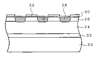
Referring to Fig.4, there is shown a plan view of a
light-receiving element array in which a light-shielding film
is provided between light-receiving elements of a diffusion-
type light-receiving element array shown in Fig.2 to prevent
the degradation of characteristic due to a stray light.>
Fig.5 is an enlarged partially cross-sectional view of the
array taken along the A-A' line in Fig.4. It should be noted
that in Figs.4 and 5 like reference numerals are used for
describing like elements in Figs.l and 2.
In this light-receiving element array, a passivation
film 30 consisting of SiN film is deposited on the structure
shown in Figs. 1 and 2 to a thickness such that a
nonreflective condition is satisfied. On the passivation
film 30, a light-shielding film 32 is provided so as to cover
the area between light-receiving elements. Openings 33 are
opened in the insulating film 30 on respective bonding pads
12 so that a wiring is bonded to each of the bonding pads.
According to the diffusion-type light-receiving element
array having the structure described above, even if the
incident light is spread with respect to the light-receiving
area or the incident light partially impinges upon outside
CA 02385086 2002-03-14
8
the light-receiving area, the incident light does not enter
the area between light-receiving elements because of the
presence of the light-shielding film 32. Therefore, carriers
are not generated in the non-depleted light-absorbing layer
24 between light-receiving elements, so that there is no
degradation of characteristic due to the lateral diffusion of
carriers.
In order to confirm the effect of the light-shielding
film, two kinds of samples were prepared to carry out a
comparison experiment. Fig.6 shows a plan view a prepared
conventional light-receiving element array, while Fig.7 shows
a plan view of a prepared light-receiving element array in
accordance with the present invention. In both samples, the
substrate was used in which n-InP, undoped (i-) InGaAs, and
n-InP were grown in turn by using an MOVPE method. A plasma
enhanced CVD SiN film was deposited on the substrate as a
passivation film. Zn was diffused from the openings provided
in the passivation film to form the diffused regions 28.
These diffused regions constituted the light-receiving areas.
The light-receiving areas each having a short side of 30,cc.m
and a long side of 100 ,u m were arrayed in a pitch of 50 ,u m.
Bonding pads 12 each electrically connected to the diffused
region 28 of each light-receiving element were positioned
alternately on both sides of the light-receiving element
array. A wiring (not shown) was bonded to the bonding pad 12.
In a light-receiving element array in accordance with
the present invention shown in Fig.7, a light-shielding film
32 were provided between light-receiving elements using a
lift-off method, the light-shielding film having the size of
20 ,u m X 100 ,u m (width X length ) and being made of a two-layer
CA 02385086 2002-03-14
9
film of Ti/Au. The light-shielding film (metal layer) was
formed by a vapor deposition using a resistance heating
method. A Ti film served for increasing the adhesion to the
SiN film, and had a thickness in the range of 50nm - 1 ,u m,
preferably of about 50nm. An Au film on the Ti film served
for shielding the light, and had a thickness of about 0.2,um.
A desirable thickness of the Ti/Au layer was totally in the
range of 0.2,um - l0,um.
Two kinds of prepared samples of a light-receiving
element were estimated by means of an optical system shown in
Fig.8. The light of 1.55,u m band (i.e., a frequency band
used in an optical communication) emitted from a single-mode
fiber 54 is collimated by means of a collimator lens 52
having a focal length of about 50mm, and impinges upon a..
diffraction grating 53. The grating period of the
diffraction grating is selected to be about 1.1,u m. The
collimated light is diffracted by the diffraction grating and
demultiplexed into a plurality of lights each having a
different wavelength. The demultiplexed lights are focused
upon respective light-receiving elements 50 of a light-
receiving element array 51 to be estimated by means of the
collimator lens 52. The light to be entered to the single-
mode fiber 54 is selected to be one wavelength. The
diffraction grating 53 is inclined to the optical axis of the
collimator lens 52 in such a manner that the output from one
light-receiving element to be measured becomes maximum, and
the position of the light-receiving element array 51 is
adjusted. In this case, the distance between the single-mode
fiber 54 and the light-receiving element 51 is selected to be
about 2.5mm in order to reduce a abaxial aberration.
CA 02385086 2002-03-14
The demultiplexing characteristic of the light-receiving
element array in accordance with the present invention in
Fig.7 is shown in Fig.9, while that of the conventional
light-receiving element array in Fig.6 is shown in Fig.lO as
5 a comparison example. In Figs.9 and 10, the ordinate
designates a relative photosensitivity (dB) and the abscissa
a wavelength (nm).
Apparent from these demultiplexing characteristics, the
conventional light-receiving element array had the crosstalk
10 of about -l5dB, whereas the crosstalk decreased to -l8dB or
less by using the light-receiving element array in accordance
with the present invention, which designated an improvement
of 3dB or more. It should be noted that the crosstalk is
determined by the relative photosensitivity at a position
where a vertical line drawn from the peak of a demultiplexing
characteristic curve of any one of demultiplexed lights
crosses to the adjacent demultiplexing characteristic curve.
For the sample shown in Fig.7, each width of the light-
shielding film and the light-receiving area is selected in
such a manner that the light-shielding film and the light-
receiving area are not overlapped, or there is no space
between them. However, this is not an indispensable
condition, and the same effect may be obtained when the width
of the light-shielding film is increased to 40,um from 20,um
or is decreased to l0,um.
While the light-receiving element array in which the
elements are arrayed in a pitch of 50,u m is used in the
sample of Fig.7, the same effect may be obtained when the
light-receiving element array in which the elements are
arrayed in a pitch of 25,um is used. In this case, the width
CA 02385086 2002-03-14
11
of a light-receiving area is selected to be 12,u m, and the
" width of a light-shielding film l3,CCm. While the width of a
light-shielding film (20,u m width) is selected in such a
manner that the light-shielding film is not overlapped to a
light-receiving element (30,(.cm width) in the sample in Fig.7,
the light-shielding film may be overlapped to the light-
receiving area if an opening remains in the light-shielding
film on the light-receiving area.
While a metal film of two-layer structure, i.e. a Ti/Au
film is used as the material of the light-shielding film in
the sample shown in Fig.7, a single-layer film such as an Au
film, a three-layer film such as a Ti/Pt/Au film, or a four
or more - layer film may be used. The metal material and the
thickness of a light-shielding film are not limited to that
illustrated in the sample of Fig.7. For example, A1 is
preferable for a passivation film because of its facility of
deposition and patterning. Also, when a carbon film of 0.2-
l0,um thick deposited by an ark vapor deposition is used in
place of a metal film as a light-shielding film, the same
effect may be obtained.
A structure for further decreasing the crosstalk in the
diffusion-type light-receiving element array will be
described hereinafter. Fig.ll shows a mesa-type light-
receiving element array in which isolation trenches are
formed by etching to electrically isolate light-receiving
elements to each other. It should be noted that in Fig.ll
like reference numerals are used for describing like elements
in Figs. 1 and 2.
Isolation trenches are etched between diffused regions,
and then a passivation film 34 is deposited on all the
CA 02385086 2002-03-14
12
surface of the structure to a thickness such that a
nonreflective condition is satisfied. A light-shielding film
36 is then deposited on the passivation film 34 except the
light-receiving areas, i.e., the light-shielding film is
deposited on the bottom and side wall of the isolating trench,
and on the top surface of the light-receiving element except
the diffused region 28. The plan view of the light-receiving
element array of the present embodiment is the same as that
in Fig.4.
According to the mesa and diffusion-type light-receiving
element array, the carriers generated in the light-absorbing
layer 24 can not migrate toward the adjacent light-receiving
elements by lateral diffusion because the light-receiving
elements are electrically isolated to each other. The light ..
obliquely impinging upon the isolating trench is shielded by
the light-shielding film 36 deposited on the side wall of the
isolating trench. Consequently, the light-receiving element
is not affected by the light that would impinge upon outside
the light-receiving area unless the light-shielding is
deposited in the isolating trench.
Therefore, in this mesa and diffusion-type light-
receiving element array, the crosstalk may be further
decreased in comparison with the diffusion-type light-
receiving element array in Fig.4.
A p-n junction is formed by diffusion in the mesa and
diffusion-type light-receiving element array. The diffusion
is isotropic, and then proceeds laterally more than a
diffusion depth. The size and array pitch of a light
receiving element array are the same as in the conventional
diffusion-type light-receiving element array.
CA 02385086 2002-03-14
13
Referring to Fig. l2, there is shown a light-receiving
element array in which a p-n junction is formed by crystal
growth in place of diffusion, and isolation trenches are
formed by etching to make a mesa-structure.
An n-TnP layer 42, an i-InGaAs layer (a light-absorbing
layer) 44, and a p-InP layer (a window layer) 46 are stacked
in turn by crystal growth on an n-InP substrate 40. The
InGaAs layer 44 and InP layer 46 are etched to form trenches
for isolating the elements to each other. A passivation film
48 is deposited on all the top surface of the structure to a
thickness such that a nonreflective condition is satisfied.
A light-shielding film 49 is then deposited on the
passivation film 48 except the light-receiving areas. The
diagram of the top surface of the light-receiving element.
array of the present embodiment is the same as that in Fig.4.
According to this light-receiving element array, a high
density integration may be possible in comparison with the
diffusion-type light-receiving element array in Fig.ll.
In the respective embodiments described above, the
light-shielding film is formed only between light-receiving
elements. However, if wirings and electrodes are further
shielded by the light-shielding film to suppress the
generation of a stray light, the device characteristic may be
improved.
Referring to Fig.l3, there is shown another example of a
mesa-type light-receiving element array which may be
fabricated by crystal growth and be integrated in a high
density. In this light-receiving element array, a light-
receiving element consists a waveguide. Fig.l3 is a
perspective view of this light-receiving element array in
CA 02385086 2002-03-14
14
which waveguide-type light-receiving elements 60 each having
a width of 6,um are arrayed in a pitch of l0,um.
This light-receiving element array may be fabricated in
the following manner. An n-InP layer 64, an i-InGaAs layer
66, and a p-InP layer 68 are grown in turn on an n-InP
substrate 62 by MOVPE and the like. At this time, the second
layer, i.e. the i-InGaAs layer 66 may be a non-doped or
lightly-doped layer.
The p-InP layer 68 and i-InGaAs layer 66 are removed to
form isolation trenches by mesa etching until the surface of
the n-InP layer 64 is partially exposed. As a result, a
waveguide structure is fabricated.
Next, an i-InP is regrown in the isolation trenches.
The isolation trenches are buried and planarlized by the :.
regrown i-InP.. In the figure, the buried region is shown by
the reference numeral 70. While i-InP is given as one
example of the material to be buried, any material may be
used which has an optical confinement effect and a sufficient
dielectric strength for adjacent light-receiving elements.
For example, an electrically insulting material such as Fe-
doped InP is more preferable. Finally, a p-type ohmic
electrode 72 is formed on the topmost layer, i.e. the p-InP
layer 68, and an n-type ohmic electrode is formed on the
bottom surface of the substrate.
In the waveguide-type light-receiving element array
fabricated in a manner described above, a p-n junction is not
formed by diffusion, so that an array pitch of light-
receiving elements may be decreased.
Also, in the waveguide-type light-receiving element
array, the light impinges upon the end face such as a
CA 02385086 2002-03-14
cleavage plane of the substrate as shown by an arrow A in the
figure. The photosensitivity of the waveguide light-
receiving element array depends on the propagation length of
the light in the InGaAs layer 66 (the light-absorbing layer).
5 On the contrary, the photosensitivity depends on the
thickness of the InGaAs layer in the diffusion-type light-
receiving element as well as the mesa-type light-receiving
element in which the light impinges upon the substrate
vertically. Therefore, in the waveguide-type light-receiving
10 element array, the length of the InGaAs layer constituting a
waveguide may be substantially larger than the thickness
thereof, so that the improvement of the photosensitivity
would be expected.
While the isolation trenches are buried by the regrowth:
15 of i-InP, they may be buried by the deposition of an
insulating film. Also, the device characteristic of the
light-receiving element array may be improved by applying a
nonreflective coating on the end surface of the substrate
upon which the light impinges.
In the waveguide-type light-receiving element array of
the present embodiment, the crosstalk may be also decreased
because the light-receiving elements are isolated to each
other by the isolation trenches.
Next, a light-receiving device in accordance with the
present invention will now be described, the device using the
waveguide-type light-receiving element array shown in Fig. l3.
This light-receiving device may be preferably applied to an
optical demultiplexer. The light-receiving device is
fabricated by mounting the light-receiving element array on a
circuit board.
CA 02385086 2002-03-14
16
One example in which the light-receiving element array
is mounted by flip chip bonding is shown in Figs .14 and 15 .
Fig. l4 is a perspective view of the light-receiving device,
and Fig. l5 a cross-sectional view for illustrating the flip
chip bonding.
An alumina substrate 82 is prepared as a circuit board.
On the alumina substrate, there are provided a pattern of
electrode wirings 83 which are formed in the same pitch as
that of p-type ohmic electrodes 72 (see the Fig.l3) in the
waveguide-type light-receiving element array to be mounted, a
plurality of leads 84 for the electrode wirings, a plurality
of bonding pads 86 connected to the leads 84, one bonding pad
88 provided near the light-receiving element array 80, a lead
90 connected to the bonding pad 88, and one bonding pad 92
connected to the lead 90. One bonding pad 92 and the
plurality of bonding pads 86 are arrayed in a straight line.
The waveguide-type light-receiving element array 80 is
mounted on the pattern of electrode wirings 83 by flip chip
bonding, for example, with the p-type ohmic electrodes 72
facing down to the pattern 83 and the n-type ohmic electrode
74 facing upward.
According to the flip chip bonding, solder bumps are
provided in advance on the pattern of electrode wirings 83 as
shown in Fig.l5, and the p-type ohmic electrodes 72 of the
light-receiving element array 80 are aligned and heat-adhered
to the solder bumps.
Therefore, the respective p-type ohmic electrodes 72
corresponding to the respective waveguides of the light-
receiving element array are connected to the bonding pads 86
arrayed on the alumina substrate 82 through the solder bumps
CA 02385086 2002-03-14
17
94, the pattern of electrode wirings 83, and the leads 84.
Also, the n-type ohmic electrode 74 of the waveguide-type
light-receiving element array 80 is connected to the bonding
pad 88 provided near the array via a bonding wire 96, the
bonding pad 88 being connected to the bonding pad 92 through
the lead 90.
If a bonding pad to be electrically connected to the
ohmic electrode 74 is formed on a light-receiving surface of
the array 80, it may be connected to the lead 90 by flip chip
bonding without using the bonding wire 96.
In the waveguide-type light-receiving element array
having the structure described above, the light impinges upon
the end surface of the substrate as shown by an arrow A in
the figure.
According to the waveguide light-receiving element array,
an electrical isolation between adjacent light-receiving
elements may easily be implemented, because a mesa-structure
is employed for a light-receiving element. As a .result, the
crosstalk between elements may be decreased and the size and
array pitch of the light-receiving element array may be
smaller.
Also, according to the waveguide-type light-receiving
element array, the light propagates not vertically but
horizontally in the light-absorbing layer, so that the area
interacting with the light becomes large to improve the
device characteristic such as a photosensitivity.
Further, according to the light-receiving device, the
waveguide-type light-receiving element array may be mounted
on a circuit board by flip chip bonding because the light
impinges upon the end surface of the substrate. In this case,
CA 02385086 2002-03-14
18
bonding pads may be provided on the circuit board, so that it
is unnecessary to form bonding pads on a light-receiving
element array chip, resulting in the reduction of the chip
size. Therefore, the number of chips obtained from one wafer
is increased.
INDUSTRIAL APPLICABILITY
According to the light-receiving element array in
accordance with the present invention, the crosstalk may be
decreased and the degradation of characteristic of a light-
receiving element array may be prevented because a light-
shielding film is provided in order that a stray light does
not impinge upon outside light-receiving areas.
Also, the carriers generated by the light do not migrate
toward adjacent elements because isolation trenches are
provided to electrically isolate light-emitting elements to
each other. As a result, the current flowing to adiacent
elements is not generated, and then the crosstalk may be
decreased and the degradation of characteristic of a light-
receiving element array may be prevented.