Note : Les descriptions sont présentées dans la langue officielle dans laquelle elles ont été soumises.
CA 02385337 2009-06-10
1
Measuring probe for measuring high frequencies and method of producing
said probe
The invention relates to a measuring probe for measuring high frequencies as
detaileci in the preamble of claim 1.
To test electronic circuits produced on wafers for example for their ability
to operate
and their electrical characteristics, use is usually made of measuring probes
which
are applied mechanically to appropriate contact points on the electronic
circuit to be
tested. Electronic circuits of this kind which need to be tested are
increasingly ones
which generate or process high-frequency signals, which means that for the
measuring probe there is an impedance of which due note needs to be taken. In
other words, the measuring probe needs to have an impedance matched to the
contact with the electrical circuit to be tested as otherwise, if there are
mismatches,
there will, as is generally known, be corresponding reflections which will
have an
unwantied effect on any measurement made or will make measurement totally
impossible. There should not even be any change in impedance over the
measuring
probe itself because jumps in impedance of this kind also cause corresponding
points
of reflection.
Hence there is known from U.S. Pat. No. 4 697 143 a measuring probe which, to
allow a constant impedance to be obtained from a measuring cable to a contact
point, has a co-planar conductor structure, with a signal conductor and a
ground
conductor being spaced away from one another in such as way as to produce a
CA 02385337 2009-06-10
2
desired constant impedance. However, this. arrangement has the disadvantage
that
due to the use of an aluminium oxide substrate complicated shielding is
required to
avoid higher-order modes. Also, the measuring probe is complicated, laborious
and
cost-intensive to produce. Because of the relevant tolerances, not every
measuring
probe produced meets the preset parameters and for this reason there is a high
scrap rate in production, which makes the measuring probe even more expensive.
In
additiori to this totally rigid arrangement of the co-planar conductor
structure having in
particular three or more conductors means that there is a problem in making
contact.
This is because, given the dimensions that exist on wafers and the
corresponding
tolerances to which the measuring probe, the contact points and the mechanical
alignment of the measuring probe are subject, it is virtually impossible
mechanically
for all the conductors in the measuring probe's co-planar conductor structure
to be
precisely in the plane of the contact points when the probe is applied to the
points.
Hence certain conductors contact their particular contact point better and
others
contact theirs less satisfactorily or not at all.
From I.I.S. Pat. No. 4 894 612 is known a measuring probe in which a
dielectric is
arranged over a complete length of a co-planar conductor structure. What is
further
disclosed is a measuring probe having strip lines where ends of the strip
lines stand
out resiliently from a substrate acting as a mounting.
The object of the invention is therefore to provide an improved measuring
probe of
the above kind, with simple and inexpensive volume production being achieved
in
this case with, at the same time, contact of a good standard.
This object is achieved by a measuring probe of the above kind having the
features
detaileci in the characterising clause of claim 1. Advantageous embodiments of
the
inventic-n are detailed in the independent claims in this case.
CA 02385337 2009-06-10
3
In a measuring probe of the above kind, provision is made in accordance with
the
invention for the dielectric to be arranged on at least one side and in
particular on
both sides of the co-planar conductor structure in a central section between,
and
spaced away from in the direction of the propagation, the co-axial cable end
and the
contact end, in such a way that each conductor in the co-planar conductor
structure
is formed to be individually free in space and resilient in relation to the
dielectric
acting as mounting between the dielectric and the contact end, a respective
gap
being formed between each pair of conductors in the co-planar conductor
structure
from the co-axial cable end to the contact end in such a way that a constant
characteristic impedance is obtained from the co-axial cable end to the
contact end.
This has the advantage that it provides an inexpensive and accurate measuring
probe vvhich can even be produced in volume and whose impedance is controlled,
thus giving low reflections when contact is made with the planar structure for
measuring purposes. The arrangement according to the invention is notable for
operatirig frequencies of up to 40 to 60 GHz, with impedance being
substantially free
of dispersion, i.e. independent of the operating frequency, over the whole of
the co-
planar conductor structure due to the design according to the invention. The
freely
resilient arrangement of the conductors in the co-planar conductor structure
between
the dielectric and the co-axial cable end ensures that there is contact of a
high
standard between all the conductors in the co-planar conductor structure and
the
corresponding contact points on a device to be tested, the standard of the
contact not
being affected by the measuring probe being tilted when it is applied to the
contact
points.
CA 02385337 2009-06-10
4
In a preferred embodiment, the dielectric is in the form of at least one block
of quartz.
To provide a secure connection between the co-planar conductor structure and
the
block of dielectric, the latter has, on a side where it is connected to the co-
planar
structure, a metal coating which substantially coincides in shape with the
latter.
To suppress higher-order modes above the desired operating frequency, the
dielectric is metallised over its full area on a side remote from the co-
planar
conductor structure. This also produces a closed, shielded structure in the
region of
the dielectric.
For ceri:ain applications, a planar circuit and in particular an electrical or
electronic i.e.
active circuit or at least one active circuit element is arranged at the co-
axial cable
end. This puts the additional circuit or the additional circuit element in the
immediate
vicinity of contacts between the measuring probe and a circuit to be tested at
the
contact end of the measuring probe.
The invention will be explained in detail below by reference to the drawings.
In the
drawings:
FIG. 1 is a perspective view of a first preferred embodiment of a measuring
probe
according to the invention,
FIG. 2 is a perspective view of a second preferred embodiment of a measuring
probe
according to the invention,
FIG. 3 is a plan view of a third preferred embodiment of measuring probe
according
to the inivention,
FIGS. 4 to 7 show successive steps in a method according to the invention, and
FIG. 8 is an S parameter plot from a simulation calculation for a measuring
probe
according to the invention.
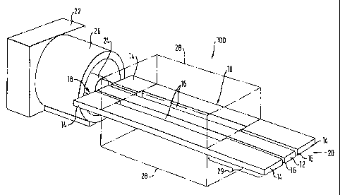
The first preferred embodiment of a measuring probe 100 according to the
invention
which is shown in FIG. 1 comprises a co-planar conductor structure 10 having a
signal conductor 12 in the centre and two ground conductors 14 arranged in co-
planar positions adjacent to the signal conductor 12. A predetermined
CA 02385337 2009-06-10
gap 16 is formed between signal conductor 12 and a given ground conductor 14.
The
co-planar conductor structure 10 extends from a co-axial cable end 18 to a
contact
end 20 and the gap 16 is formed over the entire length of the co-planar
conductor
structure 10 in such a way as to produce a constant predetermined
characteristic
5 impedance. At the co-axial cable end 18, the co-planar conductor structure
18 is
connected to a co-axial cable 22, with the signal conductor 12 making contact
with a
centre conductor 24 and the ground conductors 14 with an outer conductor 26 of
the
co-axial cable.
CA 02385337 2009-06-10
6
CA 02385337 2008-04-17
7
In a centr'al section between the co-axial cable end 18 and
the contact end 20, there is arranged on the two sides of the
co-planar conductor structure 10 a dielectric in the form of
respective blocks of quartz 28. The two quartz blocks 28 and the
co-planar conductor structure 10 are placed one on top of the
other in a sandwich-like structure. The quartz blocks 28 are
securely connected to the co-planar conductor structure 10 and
each carry on their side adjacent the co-planar conductor
structure 10 metallising which substantially matches the shape
of the co-planar conductor structure 10 in the region of the
quartz blocks 28. What is obtained in this way is a particularly
firm and close connection between the quartz blocks 28 and the
z0 conductors 12, 14 of the co-planar conductor structure 10.
Because of the electromagnetic relationship with the dielectric
28, the gap 16 is widened in the region of the quartz blocks 28
thus giving, overall, a constant characteristic impedance over
the entire co-planar conductor structure 10 from the co-axial
cable end 18 to the contact end. The respective metallisings on
the two quartz blocks 28 are advantageously connected together
electrically by means `of a suitable fitting technique. This
gives a ground plane which is identical for both sides of the
quartz blocks and a corresponding identical shielding action.
As is immediately evident from Fig.l, conductors 12, 14 are
arranged to be free in space in a region 29 between the quartz
blocks 28 acting as mountings and the contact end 20, thus
allowing each conductor to be individually resilient relative to
~.. ...... ~~~- _- -~ . ..~... 'J
CA 02385337 2002-03-19
WO 01/22097 8 PCT/DEOO/03231
its mounting in the quartz blocks 28. If the contact end 20 of
the measuring probe 100 is now pressed mechanically against
appropriate contact points for an electrical circuit to be
tested, the opportunity which each individual conductor 12, 14
in the co-planar conductor structure 10 has to be individually
resilient means that each individual conductor 12, 14 is in
optimum contact with the particular contact point assigned to
it. Any tilting of the measuring probe 100 when pressed against
the contact 'points mechanically and any tolerances to which
i0 either the conductors 12, 14 themselves or the surfaces of the
contact points are subject are compensated for by the resilient
movement of the individual canductors 12, 14. As a result of
this, a defined contact which is always the same is obtained
whenever conductors 12, 14 are applied mechanically to
is corresponding contact points, thus making it possible for
optimum measurements to be made with the measuring probe 100
according to the invention.
It is merely by way of example that measuring probe 100 is
shown with three conductors 12, 14 in a ground-signal-ground or
20 g-s-g layout. Co-planar conductor structures having only two
conductors 12, 14 or more than three conductors 12, 14 are of
course also possible, with the signal and ground conductors laid
out as follows: g-s-g-s-g-s-g ... or g-s-g-g-s-g-g-s-g-g ... or the
like. In this way it becomes possible for electrical circuits
25 for testing to be contacted with a single measuring probe which
has a plurality of co-planar signal lines.
The second preferred embodiment of a measuring probe 200
according to the invention, which is shown in Fig.2, is
substantially the same as that shown in Fig.1 and the same parts
30 are identified by the same reference numerals, thus allowing the
reader to be referred to the explanations given above in
relation to Fig.1, for descriptions of such parts. In contrast to
embodiment 100, the quartz blocks 28 have full-area metallising
CA 02385337 2002-03-19
WO Ol/22097 9 PCT/DEOO/03231
30 on a side remote from the co-planar conductor structure 10.
In the first place this metallising causes unwanted higher-order
modes above the desired operating frequency to be suppressed and
at the same time it produces a closed system over a
predetermined region of the co-planar conductor structure 10.
The third preferred embodiment of a measuring probe 300
according to the invention, which is shown in Fig.3, shows the
state which exists after the measuring probe 300 has been
produced by a method according to the invention on a silicon
wafer. In Fig.3, the same parts are once again identified by
the same reference numerals, thus allowing the reader to be
referred to, the above description of Figs.1 and 2 for
explanations of such parts. In the measuring probe 300 shown in
Fig.3 the conductors 12, 14 in the co-planar conductor structure
i5 10, having been produced by a lithographic electrofabrication
process which will be explained in detail below, are at first
connected together mechanically by a bridge 32. Formed in one
piece with bridge 32 is a frame 34 which entirely surrounds the
co-planar conductor structure 10 in one plane. By means of this
frame 34 it is possible for the co-planar conductor structure 10
to be manipulated as required until the measuring probe is
finally completed, without the conductors 12, 14 themselves in
the co-planar conductor structure 10 having to be touched, when
there would be a risk of the conductors 12, 14 being damaged.
Once the co-planar conductor structure 10 plus bridge 32 and
frame 34 which is shown in Fig.3 has been formed on a silicon
wafer by the lithographic electrofabrication process, the
arrangement 10, 32, 34 is detached from the silicon wafer and
the quartz blocks 28 are fastened to the top and bottom of the
co-planar conductor structure 10 in the appropriate region where
the gap 16 is widened, by bonding for example. From that point
on the co-planar conductor structure 10 has intrinsic strength
due to the mounting by means of the quartz blocks 28 and the
CA 02385337 2002-03-19
wo 01/22097 10 PCT/DEOO/03231
connection between the co-planar conductor structure 10 and the
bridge 32 and frame 34 can therefore be severed. This is done in
for example the region of a schematically indicated line 36. The
severing of the connection between bridge 32 and the co-planar
conductor structure 10 is advantageously performed in such a way
that outer ends 38 of the two outer ground conductors 14 project
at the co-axial cable end 18 to enable a co-axial cable for
connection to the co-planar conductor structure 10 to be
automatically located.
Conductors 12, 14 of the co-planar conductor structure 10
taper at the contact end 20 to give an arrangement for
conductors 12, 14 which is suitably matched to contact points on
an electrical circuit to be tested with which contact is to be
made. To maintain a constant characteristic impedance, the gap
16 tapers accordingly in the direction of the contact end 20 in
the region 29 at the contact end 20.
One particularly excellent property of the measuring probe
according to the invention shown in Figs.1 to 3 is that the
impedance set by the gaps 16 is substantially free of dispersion
2C over the co-planar conductor structure 10, i.e. the impedance
and phase velocity are substantially independent of the
operating frequency.
The method according to the invention of producing a
measuring probe according to the invention will be explained in
detail below in diagrammatic form by reference to Figs.4 to 7.
In a first step a layer of metal 40 is vapour deposited on a
silicon wafer 38 (Fig.4). The layer of metal compr ises for
example titanium, silver, chromium or gold. In a further step, a
light-sensitive resist 42 is applied to the layer of metal 40 as
can be seen from Fig.5. This light-sensitive resist is exposed
through a mask. The mask is so designed as to match a certain
number of co-planar conductor structures 10 to be produced on
the silicon wafer 38 together with their respective bridges 32
CA 02385337 2002-03-19
WO 01/22097 11 PCT/DEOO/03231
and their respective frames 34, as shown in Fig.3. If required,
adjacent frames are connected together mechanically. It is
particularly advantageous in this case for a large number of co-
planar conductor structures 10 as shown in Fig.3 with bridges 32
and frames 34 to be produced next to one another and one above
the other on the silicon wafer. By a photolithographic process
,
the resist 42 is thus brought into a configuration which
represents a negative of the co-planar conductor structures 10
to be produced with their respective bridges 32 and respective
ic frames 34. To do this the resist is developed in the appropriate
way. In a subsequent step, the depressions 43 which are produced
in the resist as shown in Fig.5 are filled with an electrically
conductive material 44, such as nickel for example, by
electroplating, as can be seen from Fig.6. The arrangement shown
in Fig.6 is ground down and the resist 42 is removed to give an
arrangement as shown in Fig.7. The electrically conductive
material 44 thus forms the desired structure for the co-planar
conductor structure 10 together with an individual bridge 32 and
an individual frame 34 as shown in Fig.3. Finally the layer of
2o metal 40, which acts as a dividing layer between the
electrically conductive material 44 and the silicon wafer 38, is
removed and the arrangement comprising co-planar conductor
structures plus bridges and frames lying next to one another and
one above the other can be detached from silicon wafer 38. Next,
each individual co-planar conductor structure 10 within a frame
34 is provided on both sides with quartz blocks 28 in the
appropriate region and finally the bridges 32 and frames 34 are
severed from the co-planar conductor structures 10. To conclude,
the co-planar conductor structure 10 is connected to a co-axial
30 cable at the co-axial cable end 18.
Something particularly notable about the method according
to the invention is that in no way is there a need for the
individual conductors 12, 14 in the co-planar conductor
CA 02385337 2002-03-19
WO 01/22097 12 PCT/DEOO/03231
structure 10 to be aligned in relation to one another at the
time of fitting. The arrangement of conductors 12, 14 relative
to one another is preset and fixed from the start of the
production process to the end. This gets rid of any tolerances
which might arise if the individual conductors 12, 14 were
positioned mechanically during the production process.
The measuring probe according to the invention has a
surprising good frequency response, as can be seen from Fig.8.
Fig.8 shows -an S parameter plot from a simulation calculation
Zo for a measuring probe according to the invention. What is
plotted in this case is a frequency in GHz along the horizontal
axis 46 and an S parameter in dB along the vertical axis 48. As
is immediately apparent from the graph shown in Fig.8, this
model calculation shows that the measuring probe according to
the invention can be used at frequencies of up to 60 GHz. And
this is true with, at the same time, the possibility of its
being produced in volume at low cost with a low scrap rate.