Note : Les descriptions sont présentées dans la langue officielle dans laquelle elles ont été soumises.
CA 02387432 2002-04-11
WO 01/27969 PCTIUSOO/28083
-1-
METHOD AND APPARATUS FOR ETCHING AND
DEPOSITION USING MICRO-PLASMAS
FIELD OF THE INVENTION
This invention pertains generally to the fields of plasma processing
and semiconductor manufacturing, and to plasma etching and deposition
techniques.
BACKGROUND OF THE INVENTION
Plasmas are routinely used in the manufacturing of integrated circuits
and microelectromechanical systems (MEMS). Such plasmas are used for etching
of the semiconductor substrates and for the etching or depositing of thin
films of
materials on the substrates, e.g., films of polycrystalline silicon, silicon
dioxide,
silicon nitride and metals. The reactive plasmas may be excited in a gas in
various
ways, commonly by applying a voltage across two electrodes to establish an
electric
field between the electrodes in a gas at a low pressure. The spacing between
the
electrodes is typically a few centimeters. The gas is maintained at a pressure
low
enough such that a plasma is established at a voltage between the electrodes
which
is below that at which arcing between the electrodes will take place. One of
the
electrodes may comprise the workpiece on which etching or deposition will take
place, while the other electrode may be the wall of the reactor. Typical
operating
pressures in the plasma chamber are in the range of 1-1000 millitorr,
relatively low
pressure levels that are necessary to avoid arcing during ignition of the
plasma.
The requirement for relatively low pressures necessitates the use of fairly
expensive
vacuum pumps, can require the use of load locks, and can limit the production
speed because of the time required to pump down the plasma confinement chamber
to the required pressure level.
Silicon etching in commercial plasma processing systems is
commonly performed in parallel plate reactors by applying RF power (typically
at
13.56 MHz) between two electrodes placed several centimeters apart. The
silicon
CA 02387432 2002-04-11
WO 01/27969 PCTIUSOO/28083
-2-
wafer is located on the powered electrode for reactive ion etching. The
operating
pressure and power are in the range of 10-500 mtorr and 10-500 mW/cm2,
respectively. Since the plasma exists globally across the wafer, the etch is
selectively masked by a thin film of, e.g., photoresist, SiOz or metal, which
is
patterned on the wafer surface. More recently, fast anisotropic etches have
been
demonstrated by alternative plasma etchers utilizing electron cyclotron
resonance
(ECR) and inductively coupled plasmas (ICP). All of these options, however,
employ a single plasma that acts over the entire surface area of a wafer.
Creating
several different etch depths or profiles in a single die mandates the use of
a like
number of masking steps.
A particular challenge in the use of reactive plasmas in
semiconductor processing is the need to maintain spatial uniformity in etching
or
deposition over the entire surface of the semiconductor wafer. Commercial
semiconductor wafers have diameters presently as large as 12 inches, with a
trend
toward increasingly larger wafers. To process such wafers, progressively
larger
and more expensive reactive plasma systems will be required with the use of
conventional plasma processing technology.
SUMMARY OF THE INVENTION
In accordance with the present invention, plasma treating to remove
material from a surface (e.g., etching) or to add material (e.g., deposition
or
implantation) or both can be performed over large areas of substrates, such as
semiconductor wafers, utilizing spatially localized micro-plasmas operating in
parallel with one another. A plasma can be developed in each spatially
localized
region which is tailored to the plasma treatment requirements of that region,
avoiding the non-uniformity of plasma treatment encountered with conventional
large area plasma deposition and etching systems, while permitting specific
regions
of the substrate to receive selected levels of plasma treatment independently
of other
regions of the substrate. The invention may thus be utilized, for example, to
plasma etch some regions of the substrate for longer times than other regions
with
resulting deeper etches in certain regions than in others, or to provide
etches of
CA 02387432 2002-04-11
WO 01/27969 PCT/USOO/28083
-3-
particular dimensions or patterns. In plasma etching, the power density can be
approximately 100 times higher than in conventional plasmas. In addition, DC
power can be used to etch the substrates, eliminating the need for matching
impedance networks associated with RF driven plasmas. Plasma confinement can
be varied from a few tens of microns to more than a centimeter by changing
operating conditions. The electrodes for the micro-plasmas may also serve to
mask
the etch in regions where the micro-plasma is ignited. The etch dimensions are
consequently confined to the openings in the mask, allowing as precise masking
of
the etched areas as in conventional etching. For deposition processes, the
invention
may be utilized to allow plasma mediated deposit of different materials in
various
regions of the substrate in a pattern. For example, a plasma may be
established at
certain of the spatially separated regions of the substrate while a first
precursor gas
is supplied to the region, and then a plasma may be established in other
regions of
the substrate while a second precursor gas is supplied, allowing multiple
plasma
deposition processes to take place without requiring separate lithography
masks or
removal or replacement of masks.
In the present invention, a plasma generating electrode is positioned
closely adjacent to an exposed surface of the substrate, such as above the
surface or
laterally spaced from the surface. A selected pressure of the gas in the
region of the
electrode and the substrate is established, and a voltage is applied between
the
electrode and the substrate to ignite a plasma in the region between the
electrode
and substrate for a selected period of time. The plasma is limited to the
region of
the electrode adjacent to the exposed surface so that the substrate is plasma
treated
in a pattern defined by the electrode. The electrode may be formed as
separated
electrode segments which are held over and spaced from the surface of the
substrate
so that a plasma may be established between the electrode and the substrate in
the
ambient gas surrounding the electrode and substrate. An electrode patterned in
this
manner may be selectively moved around the substrate, either continuously or
stepwise, to provide patterned etching or deposition treatment of the
substrate
surface. A single electrode may also be used as a probe to plasma treat the
substrate as the probe is moved over the surface of the substrate. The various
CA 02387432 2002-04-11
-4-
segments of the electrode may be independently supplied with voltage so that
different voltage levels may be applied between the electrodes for different
lengths
of time to tailor the amount of plasma etching or deposition at particular
locations
on the substrate. The electrode may also be formed by utilizing a dielectric
layer in
contact with the surface of the substrate with openings therein, with the
electrode
formed on the dielectric layer such that a plasma is established in the
pattern of
openings in the dielectric layer as a voltage is applied between the electrode
and the
substrate. Separate electrodes which may be separately supplied with voltage
may
be formed at or adjacent to the various openings in the substrate to allow
tailoring
of the plasmas at specific regions of the substrate. The dielectric layer and
electrode may be formed separately from the substrate and mounted onto the
substrate at a particular position at which the plasma treatments are to be
performed, removed from a position on that substrate, and then applied to a
new
substrate, or may be moved in a stepwise fashion from position to position
about a
single substrate to provide a repeated selected pattern of plasma treatment
over the
surface of the substrate. The dielectric layer may also be formed as a layer
in situ
on the substrate, with the electrode formed over it either permanently or
subject to
subsequent removal. The dielectric layer may be formed directly on the surface
of
the substrates, or a second base electrode may be formed on the substrate
surface
and the dielectric layer formed over it so that the plasma generation or
control
voltage can be applied between the upper electrode and the lower base
electrode.
An electrode formed in this manner in permanent position on the substrate may
be
_encapsulated in a casing for the substrate, e.g., a completely processed
semiconductor chip, with leads extending from the electrode and the substrate
to
leads or pins outside the casing. Electrical voltage may then be applied
selectively
to the external pins at a later time to carry out additional plasma treatment,
e.g.,
selected etching of regions of the substrate to tailor the performance of the
completed packaged unit, for example, by etching to trim the resistance of a
resistor
on the semiconductor substrate.
CA 02387432 2002-04-11
-4a-
The present invention provides a method of plasma treatment of substrates
comprising:
(a) applying a dielectric layer on a substrate surface, the dielectric layer
having
at least one opening therein that exposes the substrate surface, the
dielectric layer having
a plasma generating electrode formed thereon adjacent to the opening in the
dielectric
layer and to the surface of the substrate exposed at the opening in the
dielectric layer,
the plasma generating electrode spaced by the dielectric layer to within 1,000
m of the
substrate surface;
(b) establishing a selected pressure of a selected gas over the plasma
generating
electrode and the substrate surface; and
(c) applying a voltage to the plasma generating electrode to establish a
plasma in
the selected gas in a region between the electrode and the adjacent exposed
surface of
the substrate in the opening in the dielectric layer for a selected period of
time to plasma
treat the substrate.
The invention also provides a method of plasma treatment of substrates
comprising:
(a) positioning a plasma generating electrode adjacent to an exposed surface
of a
substrate wherein the electrode is positioned to be spaced within 1,000 m of
the
substrate surface;
(b) establishing a selected pressure of a selected gas over the plasma
generating
electrode and the substrate surface; and
(c) applying a DC voltage between the plasma generating electrode and the
substrate surface sufficient to establish a plasma in the selected gas that is
localized in a
region between the electrode and the adjacent exposed surface of the substrate
for a
selected period of time to plasma treat the substrate, wherein the gas
pressure
established over the substrate and electrode is at least 1 torr and the
electrode is
positioned sufficiently close to the substrate surface that the plasma is
established by
applying a DC voltage to the electrode at a voltage level that does not result
in arcing
and to draw positively charged ions toward the substrate surface.
The invention further provides apparatus for plasma treatment of substrates
comprising:
CA 02387432 2002-04-11
-4b-
(a) a plasma generating electrode with a flat bottom surface;
(b) a holder connected to the electrode to position the electrode bottom
surface
closely adjacent to and spaced from a surface of a substrate to within 1,000
m or less;
(c) a conductive connector to provide a conductive connection to the substrate
to
be treated; and
(d) a DC voltage source connected to the electrode and the conductive
connector
to selectively provide a DC voltage between the electrode and the substrate
surface to
establish a plasma in regions between the electrode and the surface of the
substrate so as
to draw positively charged ions toward the substrate.
The invention additionally provides micro-plasma treatment apparatus
comprising:
(a) a substrate with a surface to be treated with a plasma;
(b) a dielectric layer having a thickness less than 1,000 m mounted on the
surface of the substrate and having at least one opening therein that exposes
the surface
of the substrate at the opening; and
(c) a plasma generating electrode mounted on the dielectric layer and spaced
thereby from the substrate surface such that a plasma may be established
between the
electrode and the exposed surface of the substrate in the opening in the
dielectric layer.
In the present invention, the plasma generating electrode may be formed as
first
electrode on top of a dielectric layer, with a second plasma
.._._ _._ _ ..... .... .... .._- __T-.. ...
- - -
CA 02387432 2002-04-11
WO 01/27969 PCT/US00/28083
-5-
generating electrode also formed on top of the dielectric layer spaced from
the first
electrode by an opening in the dielectric layer. A relatively high voltage is
applied
between the two plasma generating electrodes to produce a plasma in the region
between them. At least one control electrode may be formed on the exposed
substrate surface in the region in which the plasma is generated and be biased
separately from the plasma generating electrodes to control the application of
the
plasma to the substrate. The separate control electrode allow various areas of
the
substrate to be etched or deposited at different rates or for different
lengths of time.
A particular advantage of the present invention is that the spacing
between the electrode and the substrate may be, and preferably is, small--
preferably
1000 m or less, and preferably in the range of 0.1 to 1,000 m--allowing
relatively high electric fields to be developed between the electrode and the
substrate with relatively low applied voltages. In addition, plasmas can be
developed at gas pressures that are much higher than those that are required
for
conventional plasma processing, typically at least 1 torr, while still
avoiding arcing
between the electrode and the substrate. The higher operating pressures can
also
assist in confining the plasma volume. The higher operating pressure enabled
by
the use of the present invention reduces the need for expensive vacuum pumps
and
allows shorter processing times.
The present invention allows highly tailored micro-plasmas that are
well suited to applications where etch rate, directionality and the like must
be
controlled for localized areas. The ability to separately control spatially
distinct
micro-plasmas operating in parallel with each other over a wafer surface
allows
directionality and other features of the plasma to be controlled in the
localized
regions. As an example, an isotropic etch may proceed in one region while an
anisotropic etch is performed in another region, enhancing manufacturing
throughput. Appropriate control circuitry may be utilized to control the
voltages
applied to electrode segments to separately modify the spatially separated
micro-
plasmas over time, allowing customization of the etch regions and permitting
fabrication of features that might otherwise require hundreds of lithography
steps.
Such control circuitry may, if desired, be integrated on the semiconductor
surface
CA 02387432 2002-04-11
WO 01/27969 PCTIUSOO/28083
-6-
being etched, allowing an in situ self-controlled etch. The invention may also
include circuitry for detecting the endpoint of a plasma etch or deposition
process in
a region and for terminating the etch or deposition when the desired endpoint
has
been reached.
Further objects, features and advantages of the invention will be
apparent from the following detailed description when taken in conjunction
with the
accompanying drawings.
BRIEF DESCRIPTION OF THE DRAWINGS
In the drawings:
Fig. 1 is a simplified cross-sectional view of apparatus for micro-
plasma treatment in accordance with the invention utilizing an electrode
patterned
with a dielectric layer.
Fig. 2 is a simplified cross-sectional view of another apparatus for
micro-plasma processing in accordance with the invention in which a dielectric
layer is formed in situ on the surface of a semiconductor wafer.
Fig. 3 is a perspective view of a plasma generating electrode in
accordance with the invention mounted to carry out continuous tailored etching
of
the surface of a substrate.
Fig. 4 is an exemplary layout of an electrode pattern which may be
utilized in the invention.
Fig. 5 is a simplified cross-sectional view of a further apparatus for
micro-plasma processing in accordance with the invention.
Fig. 6 is a simplified perspective view of apparatus for micro-plasma
processing in accordance with the invention of the type shown in Fig. 5.
Fig. 7 is a further simplified cross-sectional view of a portion of the
micro-plasma processing structure of Fig. 6 illustrating a single opening in
the
cathode layer under the opening in the plasma generating electrode anode
layer.
Fig. 8 is a simplified cross-sectional view of the multi-layer structure
of Fig. 6 illustrating the invention embodied with multiple openings in the
cathode
layer under a single opening in the anode layer.
CA 02387432 2002-04-11
WO 01/27969 PCT/USOO/28083
-7-
Fig. 9 is a schematic view illustrating the equipotential contours for a
structure as in Fig. 7 showing variations of the local electric field with
openings to
the substrate of varying widths (openings A, B, C) and with etch progression
(opening D).
Fig. 10 is a simplified perspective view of another embodiment of a
micro-plasma processing structure in accordance with the invention having
independent electrodes for generating the plasma and for controlling
application of
the plasma to the surface of a substrate.
Fig. 11 is a simplified perspective view, similar to Fig. 10,
illustrating the micro-plasma processing structure with separate electrodes
for
generating the plasma and separate electrodes for controlling application of
the
plasma to the substrate surface.
Fig. 12 is a perspective view illustrating the manner in which etch
profile control may be obtained when utilizing the structures of Figs. 10 and
11.
DETAILED DESCRIPTION OF THE INVENTION
The present invention may be implemented in various embodiments
to provide spatially localized regions of micro-plasmas applied to a substrate
to be
treated. In the present invention, a plasma generating electrode is positioned
closely
adjacent to an exposed surface of the substrate. The application of a voltage
between the electrode and the substrate in the presence of a selected gas at
an
appropriate pressure establishes a localized plasma in the region of the
electrode and
the adjacent exposed substrate in the pattern of the electrode. As used
herein, the
"substrate" may include a plurality of layers, including a base layer such as
a
semiconductor wafer, and other layers on the base layer. Examples of
substrates
with which the invention may be utilized include single crystal silicon,
gallium
arsenide, and other semiconductors, but the invention is not limited to
semiconductors and may be used with any other materials that are to be plasma
treated. Plasma treatment includes processes in which material is removed from
a
surface, such as surface roughening and etching, and processes in which
material is
added to a surface, such as deposition and implantation.
CA 02387432 2002-04-11
WO 01/27969 PCT/US00/28083
-8-
The plasma generating electrode in accordance with the invention
may be formed in various ways. One exemplary embodiment is illustrated with
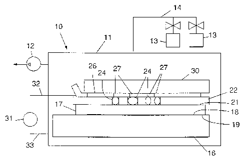
respect to the micro-plasma treatment apparatus shown generally at 10 in Fig.
1.
The apparatus 10 includes a vacuum chamber enclosure 11, a vacuum pump 12
coupled to the enclosure, and gas sources 13 connected to supply reactant gas
through valves and a line 14 to the vacuum chamber enclosure 11, all of which
may
be of standard construction for plasma processing equipment. Within the
enclosure
11 is mounted a conductive support plate 16 (e.g., of aluminum) on which is
mounted a substrate 17 (e. g. , a wafer of single crystal silicon) which is
preferably
in electrically conductive contact with the plate 16 (if desired, the
electrical contact
may be enhanced by utilization of a metal contact layer 18 in contact with the
bottom surface 19 of the substrate 17 and with the conductive plate 16). The
substrate 17 has a top surface 21 opposite to the surface 19 which is in
contact with
the electrical conductor. The top surface 21 of the substrate is the surface
to which
plasma treatment is to be applied. A dielectric spacer layer 22 is mounted on
the
surface 21 in close contact therewith. The dielectric layer 22 has at least
one
opening 24 and preferably a pattern of openings formed therein which extend
through the dielectric layer and which leave exposed the surface 21 of the
substrate
at the openings. The openings 24 define the spatially localized regions at
which
plasma treatment is to be applied to the exposed surface of the substrate. A
patterned plasma generating electrode 26 is applied over the dielectric layer
22 and
may itself have openings 27 formed therein which correspond to the openings 24
in
the dielectric layer (although they may be smaller than the openings in the
dielectric
layer as illustrated in Fig. 1). An insulating confinement layer 30 (e.g., of
glass) is
mounted over the electrode 26 to seal off the openings 27 in the electrode and
the
corresponding openings 24 in the dielectric layer. A power supply 31 is
connected
by electrical conducting lines 32 to the electrode 26 (which may be formed of
a
conductive metal such as copper or aluminum, etc.), and by a conducting line
33 to
the conductive plate 16. The power supply 31 constitutes a voltage source
which
applies a voltage to the electrode 26 and the conductive plate 16, and thereby
to the
substrate 17, to apply a voltage between the substrate 17 and the electrode
26. To
CA 02387432 2002-04-11
WO 01/27969 PCT/US00/28083
-9-
initiate processing, the pump 12 is operated to exhaust ambient gases from the
chamber 11 and reduce the pressure in the chamber to a base level, after which
the
desired reactive gas or gases are supplied from the sources 13 to the chamber
11
until a selected pressure level in the selected gas is reached in the chamber.
The application of a voltage between the electrode 26 and the
substrate 17 ignites a plasma which is established in the regions defined by
the
openings 24 in the dielectric layer 22. Depending on the reactive gas that is
provided from the sources 13 to the vacuum chamber, the plasma in the
localized
regions in the openings 24 may either etch the exposed surface of the
substrate 17
or deposit material onto the surface from the reactive gas. The result is
treatment
of the substrate in a pattern defined by the pattern of exposure of the
substrate to the
electric field from the electrode portions spaced closely adjacent thereto. In
the
embodiment of Fig. 1, the patterning of the plasma generating electrode is
determined by the pattern of openings 24 in the dielectric layer 22, which
thereby
determines the pattern in which the electric field between the electrode and
the
substrate ignites and establishes a plasma that contacts the exposed surface
of the
substrate in a corresponding pattern. The openings 27 in the electrode 26 that
are
illustrated in Fig. 1 facilitate examination and monitoring of the plasma
treatment
from a position outside the chamber 11 through a window (not shown) in the
chamber, since the plasmas confined in the openings 24 emit visible light.
However, the openings 27 in the electrode may be eliminated and a continuous
electrode used, if desired, that spans over the openings 24 in the dielectric
layer.
Ingress and egress of reactant gases to and from the openings 24 in the
dielectric
layer 22 may be obtained through laterally extending micro-channels in the
dielectric layer (not shown), by leakage between the insulating cover 30 and
the
surface of the electrode 26, or by perforations (not shown) in the insulating
cover
that lead to its upper surface.
Utilization of the insulating cover 30 is not essential, and the
formation of patterned regions of micro-plasma in accordance with the
invention
30 may be carried out without it, as illustrated by the apparatus 40 in Fig.
2. In the
micro-plasma treatment apparatus of Fig. 2, the openings 24 in the dielectric
layer
CA 02387432 2002-04-11
WO 01/27969 PCTIUSOO/28083
-10-
22 are exposed to the gas within the chamber 11 through the openings 27 in the
electrode 26. The openings 27 in the electrode 26 may be formed smaller than
the
underlying openings 24 in the dielectric layer or, as shown in Fig. 2, may
coincide
with the underlying openings. The dielectric layer 22 may be formed in situ of
a
thin layer of insulating polymer material (e.g., polyimide spun on and cross-
linked)
with the electrode 26 formed as a metal layer (e.g., nickel) deposited on the
insulating layer in a manner conventional in semiconductor processing, with
the
openings 24 and 27 formed by masking and etching steps in a conventional
manner.
The electrode 26 is thus patterned to correspond to the openings 24 in the
dielectric
layer 22 to thereby provide a patterned electric field between the electrode
and the
exposed surface of the substrate in the regions defined by the openings 24,
and
thereby to ignite and establish a plasma in the reactive gas in these regions.
A further embodiment of the invention is illustrated at 50 in Fig. 3.
For purposes of illustration, the conductive plate 16 underlying the substrate
17, the
vacuum chamber enclosure 11, the vacuum pump 12, the sources 13, and the power
supply 31 and conductive connectors 32 and 33 of Figs. 1 and 2 are not shown
in
Fig. 3, but may also be utilized for this apparatus. In the apparatus 50, the
patterned plasma generating electrode comprises two separated electrode
elements
51 and 52 which are supported in cantilevered fashion over the top surface 21
of the
substrate by a holder 54. The holder 54 may be movable to support the
electrode
segments 51 and 52 for relative motion with respect to the surface of the
substrate
16. The electrode segments 51 and 52 preferably have a flat bottom surface
(and
may be flat plates as shown) which can be positioned closely adjacent and
parallel to
the substrate surface 21. A reactive gas is supplied to the region of the
electrode
segments 51 and 52 and the substrate 17 and a voltage is applied between the
electrode segments 51 and 52 and the substrate to establish a plasma between
the
electrode segments and the substrate. The voltage may be applied to the
electrode
segments 51 and 52 by a single voltage source at a single voltage level, or
different
voltages from multiple voltage sources (or the use of voltage dividers to
provide
multiple voltage sources from a single power supply) may be supplied to the
electrode segments 51 and 52 to select the voltage that is applied between
each
CA 02387432 2002-04-11
WO 01/27969 PCTIUSOO/28083
-11-
electrode segment and the substrate. By appropriately selecting the size of
the
electrode segments 51 and 52, their spacing from the underlying surface 21 of
the
substrate, and the voltage applied to the electrode segments, the type of
treatment
that is carried out may be tailored, e.g., by operating the electrode segment
51 to
carryout an anisotropic etch in a trench 56 while operating the electrode
segment 52
to carry out an isotropic etch to form a trench 57 at the same time. The
holder 54
provides a means for moving the patterned electrodes 51 and 52 with respect to
the
substrate to provide a selected etch pattern in the underlying substrate. A
single
electrode element 51 or 52 may also be used to function as a "probe" to etch
or
deposit in a desired pattern over the surface of the substrate. Further, an
electrode
of the type 51 or 52 may be used closely spaced from the surface, as discussed
below, to plasma treat an entire substrate or a portion of it that has a
conventional
plasma masking layer applied thereto, with higher operating pressures than are
permitted with conventional plasma processing.
Fig. 4 is an illustrative plan view of two patterned plasma generating
electrodes of the type 26 shown in Fig. 2 which are formed on the surface of
the
dielectric layer 22. Each of the patterned electrodes 26 is formed as a layer
of
metal on the surface of the dielectric 22, with the coinciding openings 24 and
27 in
the dielectric layer 22 and the electrode 26, respectively, exposing the
surface 21 of
the underlying substrate. A lead segment 60 extends from each of the patterned
electrodes to a connecting pads 61 to which the electrical leads 32 may be
connected. When voltage is applied to the pad 61 under the appropriate
reactive gas
pressure conditions, a plasma will be established adjacent to the electrodes
26 both
above the electrodes and in the regions of the openings 24 and 27. In the
regions
24 and 27, the underlying surface 21 of the substrate is thus exposed to the
plasma,
while the surface areas of the substrate outside the boundaries of the
patterned
electrodes 26 shown in Fig. 4 are covered by the dielectric layer 22 and thus
protected from the plasma.
A particular advantage of the present invention is that the regions at
which the micro-plasmas are formed are preferably relatively small in
comparison
to conventional plasma processing systems. The micro-plasmas obtained in
CA 02387432 2002-04-11
WO 01/27969 PCT/US00/28083
-12-
accordance with the invention thus allow plasma deposition or implantation
with
finely controlled detail for applications such as semiconductor manufacturing.
In
addition, because of the small spacing between the electrode elements and the
exposed surface of the substrate, relatively low voltage levels (conditioned
on the
geometries of the cavities) are required to establish the plasma and much
higher
pressures in the vacuum chamber may be utilized while avoiding arcing. In the
present invention, typical preferred spacing of the patterned electrode from
the
adjacent exposed substrate surface is in the range of 0. 1 to 1,000 m.
Particularly
with in situ dielectric and electrode layers as shown in Fig. 2, preferred
spacings
can be 50 m or less. The lateral dimensions of the exposed surface features
of the
substrate which are plasma treated may also be in the same size range,
although
larger and smaller dimensions may also be utilized. Typical suitable operating
pressures are in the range of 1 to 1,000 torr, three to four orders of
magnitude
higher pressures than can be used under conventional plasma processing
conditions.
In accordance with the invention, the plasma generating electrode
(specifically its
bottom surface) is positioned very close to the surface to be treated. It is
found that
at a spacing in the range of 1000 m and less, the gas pressure required to
initiate
the plasma increases (significantly above the pressures that are used in
conventional
plasma processing) but arcing does not occur at the relatively low voltage
levels
(including DC voltages) at which the plasma will be ignited. The small spacing
between electrode and substrate permits small, localized plasmas to be formed
to
provide fine detail patterned plasma treatment as discussed above. However,
the
invention may also be used to plasma treat a large area with a single large
electrode
spaced closely adjacent to a substrate with a patterned mask thereon, while
operating at relatively high gas pressures. The size of the plasma treatment
pattern
also affects the operating pressures that are used. The size of features may
be
limited by the mean free path of the gas atom, requiring smaller features to
be run
at higher pressures. The Debye length, a function of the physical distance
required
for a plasma to shield charges, may constrain the minimum dimensions. It is
generally considered that a plasma must be several times larger than the Debye
length.
CA 02387432 2002-04-11
WO 01/27969 PCT/USOO/28083
-13-
Various power supplies 31 may be utilized to apply a suitable voltage
between the electrode and the substrate. Plasmas may be ignited utilizing any
convenient and appropriate voltage drive, including DC and switched DC
voltages,
and AC voltages including radio frequency (RF), pulsed RF, and combinations.
With respect to the illustration of Fig. 2, it is noted that the substrate
17 may comprise a semiconductor chip which is encapsulated within a casing 11
in
a conventional manner, with the conducting lines 32 and 33 extending out from
the
casing 11 as lead pins to which an external power supply 31 may be connected
at a
later time after the semiconductor has been completely processed. Electrical
connection may be made to the semiconductor (e.g., silicon) base substrate 17,
rather than through an underlying conductive plate 16 as shown in Fig. 2. In
this
manner, a completely packaged semiconductor chip may be encapsulated with a
reactant gas such that selective plasma etching or deposit may be carried out
on the
completed and packaged integrated circuit for various purposes, such as
selective
etching of a resistor channel to trim the resistance to a precise value, or to
individually compensate micromachined resonant gyroscopes for package stresses
by altering resonator mass.
Various source gases may be used as in conventional plasma
processing. Common gases used for plasma etching include nitrogen, oxygen,
argon, sulfur hexafluoride, chlorine and various chlorofluorocarbons, although
it is
understood that any of the gases used in normal plasma processing may be
utilized
for micro-plasma processing in accordance with the invention. Gases and
techniques typically used in conventional plasma deposition may also be
utilized.
For example only, two deposition processes which may be used in the present
invention are plasma enhanced chemical vapor deposition (PECVD) and
sputtering.
Sputtering is achieved by bombarding a target with energetic ions from a
plasma.
The plasma is generally formed in an "inert" gas that does not chemically
react with
the target, with nitrogen and argon being commonly used. Atoms of the target
are
knocked off and deposited on the substrate being coated. Conductors can be
sputtered with a DC plasma, as there is a conductive path to ground.
Insulating
targets will charge up, so an AC source, such as at radio frequencies, is
typically
CA 02387432 2002-04-11
WO 01/27969 PCT/US00/28083
-14-
used. Typical metals sputtered are aluminum, tungsten, titanium, and chromium,
typical semiconductors are silicon and germanium, and typical insulators are
silicon
dioxide and aluminum oxide. Virtually any element or compound can be
sputtered.
Chemical vapor deposition (CVD) relies on a chemical reaction
taking place. CVD occurs at the substrate either by thermal decomposition or
the
reaction of two or more gases. PECVD has the advantage of adding energy to the
system, to increase the reaction rates, without adding appreciable
temperature, and
thus it is particularly advantageous as a low temperature process. Typical
semiconductor materials that are PECVD deposited are silicon, silicon dioxide,
silicon nitride, and various metals. Examples of gases used in PECVD are
silane
(SiH4) for deposition of silicon, silane and oxygen for deposition of silicon
dioxide,
phosphine (PH3) and oxygen for deposition of phosphorous doped oxide, silane
and
ammonia for deposit of silicon nitride, etc. When carrying out deposition, the
electrode materials should be chosen to avoid contaminating the deposition and
to
account for chemical considerations. The substrate is typically heated for a
deposition, and this may be done locally using patterned electrodes.
The source gases from the sources 13 may be applied in a desired
sequence to the containment chamber 11 to carry out a series of processing
steps
without moving the substrate from its mount. The chamber may simply be
evacuated to a base level between each processing step before the next source
gas is
supplied to the chamber. For example, if a particular semiconductor structure
requires successive thin films of materials "A," "B" and "C" to be deposited
in
separate areas or in multiple layers, the present invention allows such
processing to
be carried out without any masking steps by selectively exciting a micro-
plasma
over each desired region while precursor gases for the materials A, B or C,
respectively, are flowing. Processing in this manner eliminates the multiple
masking steps that are required by conventional lithography based
manufacturing
methods.
Although the present invention may be utilized with conductive
substrates, such as doped silicon and other doped semiconductors, to
facilitate
application of a voltage between the patterned electrode and the substrate
surface,
CA 02387432 2002-04-11
WO 01/27969 PCT/US00/28083
-15-
the invention is not so limited and may be carried out with insulating
substrates. An
exemplary embodiment of the invention which may be utilized with either
insulating
or conductive substrates is illustrated generally at 70 in Fig. 5. The
exemplary
structures shown in Fig. 5 that are the same as in the apparatus of Fig. 2 are
similarly numbered in Fig. 5 (the vacuum chamber enclosure 11, pump 12, gas
sources 13, and supply line 14 are not shown for simplification). In the micro-
plasma processing apparatus of Claim 5, a thin film of conductive material 71
(e.g.,
a conducting metal such as nickel or copper) is applied to the top surface 21
of the
substrate 17 and is patterned with openings 72 which correspond to the
openings 24
in the dielectric layer 22. The substrate 17, which can be either conducting
or non-
conducting, is mounted on a chuck 73. The chuck 73 may be an insulator or have
an insulating layer thereon. The voltage from the voltage source 31 is
connected
through the leads 32 and 33 to the first or upper plasma generating electrode
26 and
the lower or second electrode 71, respectively, to apply a voltage between the
electrode 26 and the exposed surface 21 of the substrate at the openings 24.
With
this configuration, the voltage source 31 may be a DC voltage source to apply
a DC
voltage to ignite the plasma in the exposed regions of the substrate defined
by the
openings 22 in the dielectric layer and the openings 27 and 72 in the
electrodes 26
and 71, respectively. In this manner, etching or deposition treatment of
surfaces of
the substrate 17, which can be either insulators (e.g., glass or ceramics) or
poor
conductors such as undoped semiconductors, can be readily carried out, with
the
same advantages of the present invention as described above.
As an example of the implementation of the apparatus 70 of Figs. 5,
samples can be formed as shown in Fig. 6 by a two-mask process sequence.
First,
a metal electrode-polyimide dielectric-metal electrode stack is deposited on a
silicon
wafer forming the substrate 17. The first lithography mask is used to pattern
the
upper metal layer 26 and the polyimide dielectric layer 22. The second mask is
then used to pattern the lower metal layer 71 and simultaneously re-pattern
the
upper metal layer 26 as well. The metal layers 26 and 71 may be formed of
various
conducting metals, including chromium, aluminum, titanium, and nickel.
Following the micro-plasma etch, the electrode stack can be stripped by
sacrificing
CA 02387432 2002-04-11
WO 01/27969 PCT/USOO/28083
-16-
the lower metal electrode 71 in the appropriate wet etchant. As shown in Fig.
6,
electrical power may be supplied to the metal layers 26 and 71 utilizing pads
for the
two in situ electrodes 26 and 71, which are contacted by probes and connected
to
the DC power supply 31 through a series ballast resistor 80 which allows
control
over the plasma current. As shown in Fig. 6, the upper electrode 26 serves as
the
anode and the lower electrode 71 serves as the cathode. The lower electrode,
which
may be connected to ground, attracts the positive ions in the plasma toward
the
substrate 17, e.g., a silicon wafer. Typical bias voltages from the DC power
supply
31 range from 300 to 600 volts, depending on the ambient gas used and the
target
etch rate. Typical thicknesses of the dielectric layer 22, and thus the
spacing
between the electrode 26 and the substrate surface, is in the range of 1000 m
or
less. The silicon wafer 17 is shielded from the electric field by the grounded
cathode layer 71. The relatively small electrode areas for in situ micro-
plasmas in
accordance with the invention allow power densities in the range of 1 to 10
W/cmZ
to be achieved without drawing high currents.
Relatively high operating pressures, e.g., 1-20 torr, may be used to
spatially confine the plasma, permitting several micro-plasmas with different
etch
characteristics to operate simultaneously on a single wafer. The formation of
localized micro-plasmas is illustrated in Fig. 6 by localized plasmas 81 which
form
at the edges of the multi-layer sandwich formed by the layers 26, 22 and 71,
and by
the plasma shown at 82 formed adjacent to the openings 24 and 27 in the
dielectric
layer 22 and the upper electrode layer 26, respectively. As used herein, the
edges
of the electrodes 26 and 71 and the dielectric 22 also define an "opening" in
these
structures which exposes the substrate surface and at which a micro-plasma 81
can
be formed to treat the adjacent exposed surface. As illustrated in Fig. 6, the
micro-
plasmas 81 and 82 generally can be formed to be spatially separated from one
another and thus act independently on the underlying substrate 17. In one
example
of application of the present invention, the ambient gas used was N21 with a
bias
voltage of -360 V, which is the opposite polarity to the bias normally used
for
etching. By varying the power supplied by the DC voltage supply 31 and the gas
pressure, the plasma confinement can be changed from less than 100 m to
greater
CA 02387432 2002-04-11
WO 01/27969 PCT/USOO/28083
-17-
than 1 cm. Other samples were obtained utilizing SF6 as the gas in which the
plasma was ignited. Using this gas and performing etching through openings in
the
in situ electrodes, etches were obtained of a 92 m deep etch through a
circular
opening of 150 m diameter and a silicon substrate, achieved in 20 minutes at
2.7
torr, with a power density of 3.2 W/cm2 averaged over the electrode area. The
resulting sidewall angle was 22 off vertical. The electrode metal layers were
formed of aluminum. In another example, a 233 m deep etch was achieved in 50
minutes using the same parameters. A 33 m deep etch through a 50 m diameter
opening was achieved in three minutes at 2.9 torr and 7.3 W/cm2. The sidewall
angle was found to be nearly vertical in certain locations of the profile.
Aluminum
was also used as the electrode metal. A 207 m deep etch was made through a
280
m wide, 2.2 mm long slit opening, using metal electrodes formed of titanium.
The etch was achieved in 24 minutes at 5.2 torr and 6.8 W/cm2. The sidewall
angle
for this etch was also found to be nearly vertical in certain locations of the
profile.
It was found that varying degrees of anisotropy can be achieved by changing
the
operating conditions of the micro-plasmas. The etch rate of silicon and SF6
micro-
plasmas was also studied as a function of several operating parameters. Etches
were performed under two sets of conditions: the first set used 2.7 torr
pressure,
1.6 W/cm'` power density and aluminum electrodes with circular openings of 350
m diameter, and a second set used 5.2 torr, 6.8 W/cm2, and titanium electrodes
with 280 m wide slit openings. In the first case etch rates of 4 to 7 m/per
minute
were obtained, while in the second case etch rates of 9 to 12 m/minute were
obtained. In both cases, the etch rate was significantly higher for the first
few
minutes of the plasma treatment and then rapidly settled at a lower value that
was
stable for 50 minutes. One factor which may contribute to the higher initial
etch
rate is that the electric field above the exposed silicon is highest for the
first few
minutes of an etch, during the time that the etched depth is relatively small.
For the
second set of conditions, it was possible to etch through a wafer in less than
an
hour. Through wafer etches were readily achieved with the use of titanium
electrodes, which developed considerably less damage than aluminum from
CA 02387432 2002-04-11
WO 01/27969 PCT/US00/28083
-18-
sputtering in exposed regions of a cathode, consistent with results seen in
conventional etchers. From etches performed for three minutes at 2.7 torr
using
aluminum electrodes with circular openings to 350 m diameter, it was found
that
the etch rate increases linearly with power density over a range of electrode
power
from about 1 W/cm2 to about 7 W/cm2. The highest etch rate achieved was 17.4
gm/minute. The relatively high etch rates are facilitated in part by the high
power
densities. Since the electrode area for micro-plasmas in accordance with the
invention is generally much less than 1 cmZ, such power densities can be
achieved at
moderate current levels.
Sample etches were evaluated as a function of chamber pressure for
three minute long etches performed through a 280 m wide slit opening in
titanium
electrodes. As the pressure is increased, the power necessary to sustain the
plasma
was found to increase from 3 to 7 W/cmZ, with the ratio of the etch rate to
power
density increasing from 0.15 to 4.23 m/minute per W/cm2 as the pressure is
changed from 2 to 20 torr.
As illustrated in the simplified cross-sectional view of Fig. 7, a single
etch pattern may be formed utilizing an opening 72 in the bottom electrode
layer 71
which is substantially the same size as and generally conforms to the opening
24 in
the dielectric layer 22 and the opening 27 in the electrode 26. The exposed
surface
21 of the substrate 17 will thus be plasma etched in the entire area of the
opening
72. It is not necessary that the opening 72 in the lower electrode (cathode)
71
conform to the openings 24 and 27, or that it even be a single opening. As
illustrated in the cross-sectional view of Fig. 8, the lower electrode 71 may
have
multiple openings 72 or may have a pattern of an opening or openings which
does
not generally conform to the area of the openings 24 and 27 in the dielectric
layer
and upper electrode. The metal of the cathode electrode layer 71 forms a
barrier
that masks the areas underneath the layer from the local micro-plasma which
has
access to the surface 21 of the substrate only through the opening(s) 72. This
arrangement, which may be referred to as a shared anode configuration, is
particularly advantageous as the lateral dimensions of the etch, and thus of
the
openings, become smaller (e.g., very narrow trench widths), because it is
easier to
CA 02387432 2002-04-11
WO 01/27969 PCT/US00/28083
-19-
fabricate an electrode arrangement in which the lower metal electrode 71 by
itself is
patterned with the finer pattern of opening(s) 72 than it would be to form
similar
fine patterns of openings in both the upper electrode 26 and the dielectric
layer 22.
The variation of etch rates with lateral dimensions of the mask opening was
explored with the shared anode configuration of Fig. 8. The openings 72 in the
lower electrode 71 were 1.75 mm long and ranged in width from 106 m to 5.6
m. Three minute etches were performed at 7.2 W/cm2 power density. A 95%
reduction in slit width is found to be related to a 14% monotonic reduction in
etch
rate.
In plasmas that have a power density that is conventionally used for
semiconductor processing, ion-electron pairs are vastly outnumbered by neutral
species. As a consequence, when the applied voltage is increased, the energy
increase results in appreciably more electron-neutral collisions that electron-
electron
collisions. This results in increased plasma density but does not
substantially
increase the electron temperature. The higher plasma density then results in
larger
plasma current, which is observable as a drop in plasma resistance with an
increase
in the power density. Measurements were made for various electrode power
density levels over the range 1-7 W/cm2 at 2.7 torr using thin film aluminum
electrodes of 0.2 cm2 area to determine the measured resistance of the micro-
plasmas as a function of power density. The plasma resistance was found to
decrease with increasing power density.
Under the conditions described above, etching is believed to be
performed by ions which are pulled away from the sheath that exists above the
electrode stack by the electric field associated with the openings in the
stack.
Results from preliminary modeling of the electric field are illustrated in
Fig. 9.
These calculations of the electric field were performed using MAXWELLT"'
software, and neglect the conductivity and charge distribution of the plasma,
under
assumed conditions of openings of various widths in a 30 m thick metal-
polyimide-
metal electrode stack on a 500 m thick silicon wafer, with the relative
dielectric
constant of the polyimide being 3.5 and the resistivity of the metal being
zero. Fig.
9 shows equipotential contours which are crowded progressively closer together
in
CA 02387432 2002-04-11
WO 01/27969 PCT/US00/28083
-20-
the progressively narrower openings marked A, B and C, suggesting that the
electric fields are higher over narrow openings, while the local electric
field extends
to greater heights above the wider gaps. The difference between the contours
at
locations C and D, which are of the same width but represent shallow and deep
etches, respectively, suggest that the electric field is reduced as etch
progresses.
This decrease may be correlated to the observation that the initial etch rate
is higher
than the cumulative average rate.
In the present invention, the plasma generating electrode may be used
to generate a plasma which can be selectively applied to a substrate utilizing
independently biased control electrodes that are electrically isolated from
the
electrodes that generate the plasma. Such an apparatus is illustrated in Fig.
10. A
first plasma generating electrode 90 and a second plasma generating electrode
92
are formed on the top surface of an insulating dielectric layer 22, e.g.,
polyimide,
which is itself formed on an underlying electrode 93 on the top surface 21 of
the
substrate 17. A DC power supply 31 is connected to apply a DC voltage between
the electrodes 90 and 92 to generate a plasma in the region between the
electrodes
90 and 92. The power supplied by the DC source 31 may be at a fairly high
voltage level, e.g., 600 V. One or more control electrodes 95, which may be
patterned with openings 96 therein, are formed on the surface of the
dielectric 22
electrically isolated from each other and from the plasma generating
electrodes 90
and 92. A relatively low voltage bias may be applied between the control
electrodes 95 and the underlying electrode 93 (which itself may be either
continuous
or multiple independent electrodes) to block or pass the ion flux from the
plasma in
the region between the generating electrodes 90 and 92. By utilizing separate
power sources 98 (or separate voltages supplied from a single source)
connected to
the control electrodes 95, the etch rate or total etch time at the openings 96
in the
control electrodes can be selected to achieve different etch depths or
contours at
each control electrode opening. As illustrated in Fig. 11, the underlying
electrode
93 need not be used, and the plasma generating electrodes 90 and 92 and the
control
electrodes 95 may be formed on the surface of a dielectric layer 22 that is
applied
directly to the top surface 21 of the substrate 17. Where the bottom or
substrate
CA 02387432 2002-04-11
WO 01/27969 PCTIUSOO/28083
-21-
surface electrode 93 is utilized, it may be connected to ground to provide a
ground
plane under each of the control electrodes 95, or the substrate surface
electrode 93
may be formed of multiple independent electrodes which can be independently
biased at different levels with respect to the control electrodes 95 on the
surface of
the dielectric. The dielectric layer 22 can be, for example only, any of the
various
types of dielectrics commonly used in semiconductor processing, including
polyimide, oxide, nitride, etc. Because the control electrodes 95 can be
biased
separately and operated at relatively low voltages, while the plasma
generating
electrodes 90 and 92 are run at relatively high voltages, low voltage control
circuits,
e.g., CMOS circuitry, can be used to control the bias voltages applied to the
control
electrodes 95. As illustrated in Fig. 12, the biasing of the control
electrodes 95 can
be carried out to provide a variety of different aspect ratios during the same
etch, or
to improve the aspect ratio of the etches, as illustrated by the relatively
shallow
trench 100 between the electrode 90 and a control electrode 95 and the
relatively
deep trench 101 under the electrode 95 in the area of the opening 96.
It is understood that the invention is not confined to the particular
embodiments set forth herein as illustrative, but embraces all such forms
thereof as
come within the scope of the following claims.