Note : Les descriptions sont présentées dans la langue officielle dans laquelle elles ont été soumises.
CA 02389298 2002-04-24
WO 01/33709 PCT/USOO/41958
EXTERNALLY-DRIVEN SCHEME FOR SYNCHRONOUS RECTIFICATION
TECHNICAL FIELD
This invention relates generally to logic integrated circuits, and more
particularly to a simplified externally-driven synchronous rectification
scheme
for a DC-DC power converter, easily adapted to all types of circuit
topologies.
More particularly, the present invention provides a scheme for synchronous
rectification that simplifies the complexity of the timing circuitry.
BACKGROUND OF THE INVENTION
As logic integrated circuits (IC) have migrated to lower working
voltages in the search for higher operating frequencies, and as overall system
sizes have continued to decrease, power supply designs with smaller and
higher efficiency power modules are in demand. In an effort to improve
efficiencies and increase power densities, synchronous rectification has
become necessary for these type of applications. Synchronous rectification
has gained great popularity in the last ten years as low voltage semiconductor
devices have advanced to make this a viable technology.
Synchronous rectification refers to using active devices such as the
MOSFET as a replacement for diodes as rectifier elements in circuits.
Recently, self-driven synchronous schemes have been widely adopted in the
industry as the desired method for driving the synchronous rectifiers in
DC/DC modules for output voltages of 5 volts and below.
Most of these self-driven schemes are designed to be used with a very
particular set of topologies commonly known as "D, 1-D" (complementary
driven) type topologies. See Cobos, J.A., et a/., "Several alternatives for
low
output voltage on board converters", IEEE APEC 98 Proceedings, at pp. 163-
169. See also U.S. patent 5,590,032 issued on Dec. 31, 1996 to Bowman et
a/. for a Self-synchronized Drive Circuit for a Synchronous Rectifier in a
Clamped-Mode Power Converter, and U.S. patent 5,274,543 issued on
CA 02389298 2002-04-24
WO 01/33709 PCT/USOO/41958
Dec. 28, 1993 to Loftus entitled Zero-voltage Switching Power Converter with
Lossless Synchronous Rectifier Gate Drive. In these types of converters, the
power transformer signal in the secondary winding has the correct shape and
timing to directly drive the synchronous rectifiers with minimum
modifications.
In topologies such as the hard-switched half-bridge (HB) and the full-
bridge (FB) rectifiers, and the push-pull topologies and non-"D, 1-D" type
topologies (e.g. clamp forward with passive reset), the transformer voltage
has a recognizable zero voltage interval, making it undesirable to implement
self-driven synchronous rectification. As a result, it is necessary to use an
external drive circuit with these circuit topologies. Using the transformer
voltage to drive the synchronous rectifiers results in conduction of the
parasitic anti-parallel diode of the MOSFETs used for the synchronous
rectifiers for a significant portion of the freewheeling interval, negatively
affecting the efficiency of the module, which is undesired. Some self-driven
implementations for the resonant reset forward have been reported. See
Murakami, N. et al., "A highly efficient, low-profile 300 W power pack for
telecommunications systems", IEEE APEC 1994 Proceedings, at pp. 786-792
and Yamashita, N. et al., "A compact, highly efficient 50 W on board power
supply module for telecommunications systems", IEEE APEC 1995
Proceedings, at pp. 297-302. In these implementations, the resonant reset
interval has been adjusted to provide the correct gate-drive signal during the
freewheeling interval. Therefore, the externally-driven implementation offers
a better solution for synchronous rectification in many instances. However,
the prior art externally-driven synchronous rectification is both complex and
costly.
The implementation of an externally driven scheme for non "D, 1-D"
type topologies, for example, requires a timing network that will allow the
proper adjustment for the synchronous rectifier driving pulses relative to the
primary drive, a signal transformer or opto-coupler to transfer the timing
information between primary and secondary, an inverting stage, and a driving
-2-
CA 02389298 2002-04-24
WO 01/33709 PCT/USOO/41958
stage. The inverting stage is required to generate the proper driving pulses
for the synchronous rectifier that handles the freewheeling current. The
complexity and cost of such an external driving scheme has deterred the
electronics industry from embracing the externally driven synchronous
rectifier. Thus, what is needed is a simplified implementation of the
externally
driven synchronous rectifier.
SUMMARY OF THE INVENTION
The present invention achieves technical advantages as an externally
driven synchronous rectification scheme that can be easily adapted to all
types of topologies, but particularly adaptable to push-pull converters, two-
switch forward, conventional forward converters ( hard-switched half-bridge
(HB) and the full-bridge (FB) rectifiers), and non-"D, 1-D" type topologies
(e.g.
clamp forward with passive reset) for which no efficient externally driven
synchronous rectification scheme was previously available.
In one embodiment, disclosed is an externally-driven synchronous
rectifier circuit for a DC-DC power converter. The circuit includes a first
transformer having a primary and secondary winding, the secondary winding
having a first terminal and a second terminal. The circuit includes a first
synchronous rectifier, having a gate, coupled to the second terminal of said
first transformer and having a control terminal, and a second synchronous
rectifier coupled to the first terminal of said first transformer and having a
control terminal. An external drive circuit includes a second transformer
having a primary and secondary winding, the secondary winding having a first
and second terminal. A first switch is controllably coupled to the second
synchronous rectifier control terminal, and a second switch is also
controllably
coupled to the second synchronous rectifier control terminal. The circuit
further comprises an inductor in series with the first terminal of the first
transformer and the voltage out terminal and a capacitor in parallel with the
inductor. Because the first synchronous rectifier is not coupled to the second
-3-
CA 02389298 2002-04-24
WO 01/33709 PCT/USOO/41958
transformer, only the second synchronous rectifier can receive timing
information from the external drive circuit.
In another embodiment, disclosed is an externally-driven synchronous
rectifier circuit for a DC-DC power converter. The circuit, similar to the
embodiment described above, further comprises a third and fourth switch, the
third switch coupled to the second synchronous rectifier and the fourth switch
coupled to the first synchronous rectifier. Each switch contains a gate,
drain,
and source. The secondary winding of the second transformer comprises a
center tap connected to the voltage out terminal. The gate of the first switch
is connected to the first end of the secondary winding of the second
transformer while the gate of the second switch is connected to the second
end of the second transformer, therefore both switches can receive timing
information from the external drive circuit and thus both synchronous
rectifiers
can receive timing information from the external drive circuit.
Other embodiments of the present invention include implementation as
a full wave rectifier. Further embodiments include utilizing current limiting
resistors for limiting the drive current of the circuit, additional switches
for
limiting the gate voltage, and additional capacitors for minimizing voltage
overshoot across the synchronous rectifiers.
Also disclosed is a method of rectifying a varying DC signal of a DC-
DC power converter using an externally driven synchronous rectifier circuit
with a transformer having a primary winding and a secondary winding, where
the secondary winding has a first and second terminal. The method includes
the steps of providing the varying DC signal to the primary winding of the
transformer, a first synchronous rectifier controllably conducting current via
a
second terminal of the second winding and a first switch controlling the first
synchronous rectifier. A second synchronous rectifier controllably conducts
current via the first terminal of the second winding, and a first switch
controls
the second synchronous rectifier, wherein the first and second synchronous
-4-
CA 02389298 2002-04-24
WO 01/33709 PCT/USOO/41958
rectifiers conduct when a voltage across the secondary winding is
approximately zero.
BRIEF DESCRIPTION OF THE DRAWINGS
The above features of the present invention will be more clearly
understood from consideration of the following descriptions in connection with
accompanying drawings in which:
Figure 1A illustrates a prior art conventional forward converter with
externally driven synchronous rectification in which one synchronous rectifier
is driven;
Figure 1 B illustrates a prior art conventional forward converter with
externally driven synchronous rectification in which both synchronous
rectifiers are driven;
Figure 1 C shows voltage waveforms of the self-driven synchronous
rectifier of the prior art for a conventional forward converter circuit with
externally driven synchronous rectification;
Figure 2A illustrates a forward converter with externally driven
synchronous rectification in which one synchronous rectifier is driven
utilizing
an embodiment of the present invention;
Figure 2B illustrates a forward converter with externally driven
synchronous rectification in which both synchronous rectifiers are driven
utilizing an embodiment of the present invention;
Figure 3 illustrates a full wave rectifier with externally driven
synchronous rectification utilizing an embodiment of the present invention;
-5-
CA 02389298 2002-04-24
WO 01/33709 PCT/US00/41958
Figures 4A and 4B illustrate an implementation of an externally driven
synchronous rectifier for a full bridge topology utilizing an embodiment of
the
present invention;
Figure 4C shows voltage waveforms of the externally driven
synchronous rectifier for a full bridge topology during conditions where
negative current flows through the output inductor;
Figure 5 shows experimental waveforms of a dc/dc converter using the
full bridge implementation synchronous rectifier of the present invention;
Figure 6 shows embodiment of the present self-driven synchronous
full-wave rectifier having gate voltage limiting MOSFETs; and
Figures 7A and 7B show another embodiment of the present invention
with capacitors to reduce voltage overshoot across the synchronous rectifiers.
Corresponding numerals and symbols in the different figures refer to
corresponding parts unless otherwise indicated.
DETAILED DESCRIPTION OF PREFERRED EMBODIMENTS
The following is a description of the structure and method of the
present invention. A prior art circuit will be discussed first, followed by a
description of several preferred embodiments and alternatives of the present
invention, and a discussion of the advantages.
One problem with applying synchronous rectification schemes to a
conventional forward topology is that the synchronous rectifier which
conducts during the freewheeling stage turns off before the freewheeling
stage ends. Furthermore, if a MOSFET is used for the synchronous rectifier,
the parasitic anti-parallel diode of the MOSFET conducts, increasing the
losses. It is necessary for the MOSFET to remain on and conduct during the
-6-
CA 02389298 2002-04-24
WO 01/33709 PCT/USOO/41958
entire freewheeling stage to effectively implement a synchronous rectification
scheme for these types of converters, and to obtain high efficiency. The
externally-driven circuitry allows for the proper driving pulse to be
generated
for a synchronous rectifier. The prior art has established a solution to the
freewheeling current problem.
Referring to Figures 1A and 1B, therein is illustrated an externally-
driven synchronous rectification circuit 10 of the prior art used in a
conventional forward topology with a corresponding timing diagram of the
voltage waveforms shown in Figure 1 C. The timing signals for first
synchronous rectifier SQ1 is derived from the primary transformer 16 while
synchronous rectifier SQ2 derives its timing signals from the external drive
circuit 18. The primary transformer 16 has a primary and secondary winding,
and 22, respectively.
As such, some of the timing information for the synchronous
rectification circuit 10 is obtained by transferring the information from the
primary winding 20 to the secondary winding 22. The secondary winding 22
has a first terminal 24 and a second terminal 26. The timing information is
transferred to first synchronous rectifier SQ1 by coupling the gate of first
synchronous rectifier SQ1 to the second terminal 26. Likewise, second
synchronous rectifier SQ2 receives its timing information from the external
drive circuit 18 which includes a timing circuit 28 and a second transformer
30. The second transformer 30 has a secondary winding 32 which has a
first terminal 34 and a second terminal 36. The second transformer primary
winding 31 receives the timing information and transfers that information to
the secondary winding 32. The first terminal 34 of the second transformer 32
is connected to the gate of second synchronous rectifier SQ2. As shown in
figure 1A, gates 38a and 38b may be used to drive the gate of second
synchronous rectifier SQ2.
-7-
CA 02389298 2002-04-24
WO 01/33709 PCT/US00/41958
A second embodiment of a prior art synchronous rectifier circuit 12 is
shown in Figure 1 B which utilizes the external drive circuit 18 to provide
timing information to both synchronous rectifiers SQ1 and SQ2. The second
synchronous rectifier circuit 12 is similar to the synchronous rectification
circuit 10 described above with the exception that the gate of first
synchronous rectifier SQ1 is connected to the first terminal 34 of the second
winding 32, just as second synchronous rectifier SQ2 is connected, to receive
its timing information. Figure 1 C illustrates the gate-to-source voltage
waveforms for first synchronous rectifier SQ1, the second synchronous
rectifier SQ2, and the switch Q1 as a function of the voltage across the
primary transformer 16.
While the prior art rectifier circuits 10 and 12 provide the necessary
timing for the synchronous rectifiers SQ1 and SQ2 to ensure correct on and
off switching, these implementations are both complex and expensive.
Because of the complexity and cost, the prior art synchronous rectification
circuits 10 and 12 have not been embraced by industry for numerous
applications. The present invention provides a simplified implementation of
the externally-driven synchronous rectifier circuit where the circuit's
complexity and cost have been reduced. Furthermore, the present invention
provides other advantages including eliminating disabling of the synchronous
rectifiers SQ1 and SQ2 when current tries to flow from output to input
generally causing the destruction of the synchronous rectifier circuits 10,
12.
The present invention provides a less complex and costly solution as
compared to prior art synchronous rectifier circuits 10 and 12 by adding a
first
driving circuit 52 comprised of two switches SQ3 and SQ4, as shown in the
forward converter synchronous rectifier circuit with passive reset layout 50
of
Figure 2A. Preferably, switches SQ3 and SQ4 are MOSFETs smaller than
the MOSFETs used as synchronous rectifiers SQ1 and SQ2. The switches
SQ3 and SQ4 are used to drive synchronous rectifier SQ2. As shown in
-8-
CA 02389298 2002-04-24
WO 01/33709 PCT/US00/41958
Figure 2A, the inverting stage and driving circuit 52 have been merged
utilizing switches SQ2, SQ3 and SQ4.
According to the present invention, synchronous rectifiers SQ1 and
SQ2 are turned off when the voltage of the primary transformer 16 switches
polarity. Synchronous rectifier SQ2 is turned on through the anti-parallel
diode Dl. The timing circuit 18 is not used to turn-on the synchronous
rectifiers SQ1 and SQ2 as the timing information is derived from the primary
transformer 16. Synchronous rectifier SQ2 is coupled to the timing circuit 18
to provide the proper turn-off timing. Therefore, the timing circuit 18 can be
much less complicated compared to those used with synchronous rectifier
circuits 10 and 12. The inductor Lo is coupled in series between the first
terminal 24 and the output voltage terminal 48 to smooth current ripples with
capacitor Co across the voltage terminal 48 to smooth the output voltage Vo.
An additional advantage of the present externally driven synchronous
rectification circuit 50 is that the additional switches SQ3 and SQ4 act as an
active damper to the gate drive signal used to drive the rectifier SQ2. The
switches SQ3 and SQ4 provide a buffer to the gate signal of the synchronous
rectifier SQ2 from the parasitic oscillations that normally appear in the
secondary winding 22 of the primary transformer 16 due to the interactions of
stray inductances and the output capacitance of the semiconductor devices.
Figure 2B illustrates another embodiment of a synchronous rectifier
circuit 55, according to the present invention in which neither synchronous
rectifiers SQ1 and SQ2 is self-driven. Again, the inverting and driving stages
have been merged into first and second driving stages 52 and 57, as
represented by switches SQ3, SQ4, SQ5 and SQ6. Specifically, switches
SQ3 and SQ4 are used to provide the turn-off voltage from the external drive
circuit 18 to the synchronous rectifier SQ2. Some of the timing information
from the primary transformer 16 is utilized to provide the turn-on voltage for
the synchronous rectifiers SQ1 and SQ2. Since the external drive circuit 18
-9-
CA 02389298 2002-04-24
WO 01/33709 PCT/USOO/41958
provides only the turn-off time of the rectifiers SQ1 and SQ2, the complexity
of the timing circuitry 28 is significantly reduced.
The implementation of the present invention for use with a full-wave
rectifier is similar to that of the half-wave rectifier as shown and denoted
generally as 60 in Figure 3. However, the turn-off of the synchronous
rectifiers SQ1 and SQ2 is determined from the signal from the second
transformer 30 of the external drive circuit (not shown in Figure 30) and the
turn-on timing is determined from the voltage generated from the primary
transformer 16. If this driving scheme is implemented in topologies like the
push-pull, half-bridge, or full-bridge topologies an interesting phenomena is
observed for conditions that traditionally result in reversal of power flow
that
eventually destroy the power module. The full wave rectifier 60 of the present
invention comprises a self-correcting mechanism that prevents the current
from building in the opposite direction.
In the present invention, during conditions where there is a reversal of
power flow, the current through the inductor Lo decreases and becomes
negative, thus the current through the active switches SQ1, SQ2, SQ3, and
SQ4 also changes polarity and flows through their anti-parallel diodes.
Therefore, when the switches SQ1 and SQ3 attempt to turn off, nothing
happens since current continues to flow in their anti-parallel diodes.
Effectively, switches SQ1 and SQ3 will not turn off until their anti-parallel
diode is naturally commutated off. The anti-parallel diodes will finally turn
off
when the summation of the reflected load current and the magnetizing current
is equal to zero or slightly positive. Thus, the second synchronous rectifier
SQ2 does not turn on until the voltage of the primary transformer 16 vanishes
to zero so that no conflicting condition is developed. Generally this self-
correcting mechanism works only for push-pull topologies because the turn
off of the switches SQ1, SQ2, SQ3, and SQ4 like in most other topologies
does not determine the turn-off of the synchronous rectifiers SQ1 and SQ2.
-10-
CA 02389298 2002-04-24
WO 01/33709 PCT/US00/41958
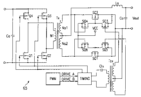
Figure 4A illustrates the implementation of an externally driven
synchronous rectifier circuit for a full-bridge topology, denoted generally as
65, and the corresponding voltage waveforms for the conditions where there
is a reversal of power flow in a full-bridge topology in Figure 4C. These
conditions may develop with two or more modules in parallel where a very
loose current sharing scheme is used during the turn-on phase of a module
while another module is already on (or module start-up into a working voltage,
hot plug-in). For implementations where the external drive circuit 18 defines
both the turn-on and turn-off times of the synchronous rectifiers SQ1 and
SQ2, a typical synchronous rectifier would not be allowed to self-correct and
both synchronous rectifiers SQ1 and SQ2 would conduct as soon as the
switches turn off allowing the inductor current to build in the negative
direction. Eventually, the inductor Lo current would grow in the negative
direction to a magnitude such that the module would fail. Even if the module
does not fail this is not a desirable mode of operation from a systems point
of
view.
For D and 1-D type topologies, this problem is more severe since a
small negative current will result in "shoot-through" in the primary switches
that can easily lead to a module failure. In general, an oring diode is needed
when paralleling modules with synchronous rectification. More complex
solutions would disable the synchronous rectifiers SQ1 and SQ2 when the
inductor current goes negative. This suggests that an accurate means of
measuring this current and a fast acting disabling circuit is needed.
Figure 5 shows the waveforms of a dc/dc converter using the full
bridge synchronous rectifier 65 of the present invention to drive a 3.3 V bus
in
the absence of an oring diode and active current sharing. Trace 1 shows the
output voltage; trace 2 shows the output current; trace 3 shows the gate-drive
of the synchronous rectifiers SQ1 and SQ2, and trace 4 shows the secondary
bias voltage. It can be seen that the output current (trace 2) of the dc/dc
module goes slightly negative initially before it builds up, thus confirming
the
-11-
CA 02389298 2002-04-24
WO 01/33709 PCT/USOO/41958
expected self-correcting characteristics of the full wave synchronous
rectifier
65.
If shoot-through currents interfere with the normal operation of the
circuit 65, optional resistors R1 and R2 may be added, as shown in Figure
4B. Again, the inverting and driving stages have been merged into one by
using a p-FET in switches SQ4 and SQ6 and n-FET devices in switches SQ3
and SQ5. Due to the turn-on and turn-off characteristics of these devices,
shoot-through currents will develop in the external driver circuit during turn-
on
and turn-off. The addition of limiting resistors R1 and R2 in series with the
p-
FET devices, switches SQ4 and SQ6, will minimize the effects of shoot-
through currents.
In most practical applications, it is necessary to clamp the gate-drive
signal to a predetermined value in order not to exceed the breakdown voltage
of the gate. The voltage of synchronous rectifier circuits 10 and 12 is
generated from the rectified peak transformer voltage resulting in a supply
voltage that is susceptible to input voltage variations. An embodiment of the
present invention which limits the gate voltage to a predetermined value is
shown in Figure 6. In this implementation, a pair of voltage limiting switches
SQ7 and SQ8, preferably comprising N-type MOSFETs have been added to
limit the voltage on the gate of the synchronous rectifiers SQ1 and SQ2 to
VCCS2-gate minus the threshold voltage (1 to 2 volts).
Implementing this driving scheme for the conventional half-wave and
full-wave rectifier configurations may result in a float gate voltage for the
synchronous rectifiers SQ1 and SQ2. Therefore, level shifting into the gate
signal of the drive switches is needed. Level shifting of the drive voltage
into
the drive switches is shown in Figures 7A and 7B. Capacitors CC2 and CC3
provide a snubbing mechanism to minimize voltage overshoot across the
synchronous rectifiers and a bias voltage for the timing circuitry 18 of
synchronous rectifiers SQ1 and SQ2.
-12-
CA 02389298 2002-04-24
WO 01/33709 PCT/USOO/41958
The novel method and system of the present externally-driven
synchronous rectifier schemes provide the advantage of efficiently providing
externally-driven synchronous rectification for a DC-DC power converter,
where the synchronous rectifier conducts when a voltage across the
transformer secondary winding is approximately zero. A further advantage of
the present invention is the ability to adapt the scheme for a variety of
converter topologies. Another advantage of the present invention is that the
switches SQ3 and SQ4 act as an active damper to the gate drive signal,
providing a buffer to the gate signal of the synchronous rectifiers from
parasitic oscillation, eliminating the need for additional components for
minimizing this effect.
While the invention has been described with reference to illustrative
embodiments, this description is not intended to be construed in a limiting
sense. Various modifications in combinations of the illustrative embodiments,
as well as other embodiments of the invention, will be apparent to persons
skilled in the art upon reference to the description. For example, the
synchronous rectifiers SQ1 and SQ2; switches SQ3, SQ4, SQ5, and SQ6;
and voltage drivers SQ7 and SQ8 are shown as MOSFETs; however, it is
contemplated that another type of FET or switching device would be suitable
for use in the present invention. It is therefore intended that the appended
claims encompass any such modifications or embodiments.
-13-