Note : Les descriptions sont présentées dans la langue officielle dans laquelle elles ont été soumises.
CA 02389456 2002-06-06
TRW Docket No. I2-1110
ASYMMETRICALLY BIASED HIGH LINEARITY BALANCED AMPLIFIER
BACKGROUND OF THE INVENTION
1. Field of the Invention
[0002] The present invention relates to a power amplifier and more
particularly to a
microwave power amplifier topology that provides high output power with good
phase and
amplitude linearity at relatively high output power levels across a relatively
wide frequency
range.
Z. Description of the Prior Art
[0003] Radio frequency and microwave communication systems are known to place
ever-
increasing demands on the linearity and efficiency of power amplifiers.
Unfortunately,
conventional power amplifiers operate at maximum efficiency at or near
saturation. Thus, in
order to accommodate communication signals having varying amplitudes, systems
utilizing
Z
M~ . PiL ~~I I y ~ ;,
CA 02389456 2002-06-06
TRW Docket No.12-1110
conventional power amplifiers normally operate at less than peak efficiency
for a substantial
portion of the time.
[0004] In order to solve this problem, so-called Doherty amplifiers have been
developed.
Doherty amplifiers were first introduced by an inventor having the same name
in; "Radio
Engineering Handbook" 5~' edition, McGraw Hill Book Company, 1959, pp. 18-39,
as well as
U.S. Patent No. 2,210,02$. The standard topology for a Doherty amplifier
includes a carrier
amplifier, operated in a Class AB mode and peak amplifier operated in a Class
C mode. A
quadrature Large coupler is used at the input so that the carrier amplifier
and peak amplifier
signals will combine in phase. A quarter wave amplifier is provided at the
outputs of the
amplifier. In essence, the carrier amplifier operates at a point where the
output begins to saturate
for maximum linear e~ciency. The peak amplifier is used to maintain the
linearity of the output
signal when the carrier amplifier begins to saturate.
[0005] Such Doherty amplifiers have been known to be used in various microwave
and RF
applications. Examples of such applications are disclosed in U.S. Patent NO.
5,420,541;
5,880,633; 5,886,575, 6,097,252 and 6,133,788. Examples of such Doherty
amplifiers are also
disclosed in "A Fully Integrated Ku-Band Doheriy Amplifier MMIC," by C. F.
Campbell, IEEE
Mise and-Guided W~ve_ Letters. YQI. 9, No. 3, March 1999, pp. 114-116; "An 18-
21 GHz
InP DHBT Linear Microwave Doherty Amplifier", by Kobayashi et al, 2000 IEEE
Radio
Frequency Inte~,rated Circuits S~rmnosium D:gest of Pagers, pages 179-182; "A
CW 4 Ka-Band
Power Amplifier Utilizing MMIC Multichip Technology," Matsunaga, et al,, 1999,
GaAs IC
Symposium Digest, Monterey, California, pp. 153-156, all hereby incorporated
by reference.
[0006] The systems mentioned above are known to provide relatively good phase
linearity
and high efficiency since the power amplifier need only respond to constant or
near constant RF
amplitude envelopes. Unfortunately, the RF amplitude envelopes of mufti-
carrier signals (multi-
frequency signals) change with time as a function of the bandwidth. Power
amplifiers utilized in
mufti-carrier systems must be able to operate over a relatively large
instantaneous bandwidth
while providing relatively good phase linearity for RF signals having non-
constant envelopes.
One attempt to provide a power amplifier suitable for mufti-carrier
applications is disclosed in
U.S. Patent No. 5,568,086. The '086 patent discloses a Doherty-type amplifier
and includes a
carrier amplifier and a peak amplifier. The amplifier is configured such that
the carrier amplifier
2
CA 02389456 2002-06-06
TRW Docket No. 12-1110
saturates at half of its maximum power level. In addition, the amplifier
includes a number of
phase shifting components.
[0007] There are several drawbacks to the mufti-carrier Doherty amplifier
disclosed in the
'086 patent. First, the carrier amplifier is only operated to one half of its
maximum power
capability, which results in lower efficiency and linearity. Second, the power
amplifier is
relatively complex including a number of phase shifting components. Thus,
there is a need for
simplified mufti-carrier microwave amplifiers, which provide good phase and
amplitude linearity
at relatively high output power levels across a relatively wide frequency
range.
SUMMARY OF THE INVENTION
[0008] The present invention relates to a microwave amplifier and more
particularly to a
microwave amplifier configured as a Doherty amplifier. The amplifier includes
a carrier
amplifier, a peak amplifier, a Lange coupler at the input of the amplifiers
and a quarter wave
amplifier at the output of the amplifiers. In order to improve isolation
between the amplifiers to
minimize the dependence of each amplifier's inter-modulation (IM) performance
on the others,
matching networks are provided, coupled to the output of the amplifiers. In
addition, the
microwave power amplif er includes electronic tuning which allows for improved
inter-
modulation distortion over a wide input power dynamic range which allows the
IM performance
of the microwave amplifier to be adjusted for the operating frequency of the
amplifier.
DESCRIPTION OF THE DRAWINGS
[0009] These and other advantages of the present invention will be readily
understood with
reference to the following specification and attached drawing wherein:
[0010] FIG. 1 is a schematic diagram of the microwave power amplifier in
accordance with
the present invention.
[0011] FIG. 2 is a graphical representation of the output power as a function
of the gain for
various biasing points of the carrier and peak amplifiers forming the
microwave power amplifier
in accordance with the present invention.
[0012] FIGs. 3A-3C illustrate matching networks for use with the present
invention.
[0013] FIGs. 4A-4B illustrate biasing networks for use with the carrier and
peak amplifiers
of the present invention.
3
~I ~ ~, ' r r GI
CA 02389456 2002-06-06
r...' .
TRW Docket No.12-1110
DETAILED DESCRIPTION OF THE INVENTION
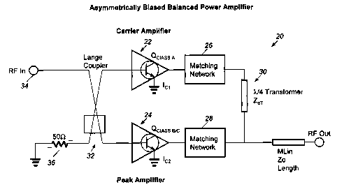
[0014) The present invention relates to a microwave power amplifier configured
as a
Doherty amplifier, generally identified with the reference numeral 20. The
microwave power
amplifier 20 includes a carrier amplifier 22 and a peak amplifier 24. Both the
carrier amplifier
22 and the peak amplifier may be formed from heterojunction bipolar
transistors (HBT) 22 and
in particular as a prematched 1.5 x 30 pmt x four finger DHBT device with a
total emitter area of
180 Eun2. An example of such .a device is disclosed in "An 18-21 GHz InP DHBT
Linear
Microwave Doherty Amplifier", by Kobayashi et al, 2000 IEEE Radio Frequency
Intesrated
Circuits Symposium Digest of Papers, pages 179-182, hereby incorporated by
reference.
Methods for fabricating HBTs are extremely well known in the art, for example,
as disclosed in
commonly owned U.S. Patent Nos. 5,162,243; 5,262,335; 5,352,911; 5,448,087;
5,672,522;
5,648,666; 5,631,477; 5,736,417; 5,804,487; and 5,994,194, all hereby
incorporated by
reference.
[0015] In order for the output signals from the carrier amplifier 22 and the
peak amplifier 24
to be in phase at the output, a Lange coupler 32 is provided. One input
terminal of the Lange
coupler 32 is used as a RF input port 34. The other input terminal is
terminated to an input
resistor 36. One output terminal of the Lange coupler 32 is coupled to the
input of the carrier
amplifier 22 while the other output terminal is coupled to the input to the
peak amplifier 24. A
1/4-wave impedance transformer having a characteristic impedance Zo = 2RL +
Ropy is provided
at the output of the amplifiers 22 and 24. An output terminal of the power
amplifier 20 is
terminated to load impedance R~. Both the carrier amplifier 22 and the peak
amplifier 24 are
configured to deliver maximum power when the load impedance RL is RQP~.
[0016] The carrier amplifier 22 is operated as a Class A amplifier while the
peak amplifier
24 is operated as a Class BlC amplifier. In order to improve the isolation
between the carrier
amplifier 22 and the peak amplifier 24, for example, when the carrier
amplifier 22 is biased as a
Class A amplifier and the peak amplifier 24 is biased between Class B and C,
matching networks
26 and 28 are coupled to the output of the carrier amplifier 22 and the peak
amplifier 24. As
such, the impedance of each amplifier stage will not contribute to the inter-
modulation (IM)
performance of the other stage.
4
dl I II I ~I ~ I RI I I
CA 02389456 2002-06-06
TRW Docket No.12-1110
[0017] In order to fully understand the invention, a discussion of known
Doherty type
amplifiers is presented first. More particularly, as set forth in: "A Fully
Integrated Ku-Band
Doherty Amplifier MMIC," supra, the loading impedance presented to the carrier
and peak
amplifiers of known Doherty amplifiers is a function of the output power
delivered by the peak
amplifier. During low input drive levels (i.e. levels in which the 1Zf input
amplitude is low), the
peak amplifier is turned off resulting in a configuration in which the can'ier
amplifier saturates at
a relatively low input drive level. As such, the carrier amplifier will result
in a higher power
added efficiency (PAE) at lower input power levels. As the input power level
increases, the peak
amplifier will begin to turn on as the power delivered by the peak amplifier
increases. The load
presented to the carrier amplifier decreases allowing the carrier amplifier 24
to increase to
provide power to the load.
[0018] The matching networks 26 and 28 are serially coupled to the outputs of
the carrier
and peak amplifiers 22 and 24, respectively. These matching networks 26 and 28
may be
provided as low pass networks, for example, as illustrated in Figs. 3A-3C. As
shown in Figs.
3A-3C, the matching networks 26, 28 may be implemented as a series inductance
40 or
transmission line 42 and a shunt capacitance 44 or open stub 46. In operation,
when the carrier
amplifier 22 is on and the peak amplifier 24 is off, the matching networks 26,
28 provide a
relatively high impedance (mainly due to the high impedance transmission line
42 or inductance
40) such that the peak amplifier 24 does not load down the carrier amplifier
22, operating in class
A, to achieve optimum linearity and efficiency under low input power
conditions.
[0019] The theory of operation of the matching networks 26, 28 is contrary to
the operation
of matching networks used for conventional power amplifiers. More
particularly, typically in a
power amplifier application, a low impedance series transmission line or low
impedance shunt
capacitance or open stub is provided at the output of the power transistor in
order to efficiently
transform the low impedance of the power transistor to a higher manageable
impedance as well
as provide isolation between the amplifying transistors.
[0020] In accordance with another aspect of the invention, the carrier
amplifier 22 and peak
amplifier 24 are DC biased tuned so that the optimum IM performance can be
achieved for the
specific operating frequency of the amplifier. For example, for a 21 GHz
carrier frequency, a
microwave amplifier 20 can be DC biased tuned to minimize the IM performance
at 20 GHz.
. ii 1e Imt !~ I fl i
CA 02389456 2002-06-06
TRW Docket No. 12-1110
[0021] FIG. 2 illustrates the measured gain and IM3 (third order modulation
products) as a
function of output power at 21 GHz . for various biasing conditions of the
amplifier 20. In
particular, the IM3 and gain is illustrated for Class A bias operation (Icl =
64mA; Ic2 = 64 mA)
as well as asymmetric bias conditions. In particular, the asymmetrically bias
conditions are
illustrated when the peak amplifier 24 is off and the carrier amplifier 22 is
biased in a Class A
mode (IC1 = 60-64 mA) and the peak amplifier is bias in Class B (IC2 = 0.3-10
mA). As
illustrated in FIG. 2, adjustment of the peak amplifier bias current (IC2)
allows the shape and
perfon~aance of the IM3 linearity ratio to be significantly improved across a
relatively wide
output power range. During a biasing condition (i.e. Icl = 60 mA; Ic2 = 0.3
mA), when the peak
amplifier is nearly shut off, the microwave power amplifier 20 in accordance
with the present
invention achieves a relatively dramatic improvement of the IM3 ratio
resulting in a deep IM3
cancellation of about -43 dBc. For mufti-carrier communication systems, an IM3
ratio of about
30 dBc is a typical requirement for linearity. With such linearity, the
microwave power
amplifier 20 is able to achieve about 20% power added efficiency (PAE) and an
output power of
about 20.1 dBm which is a significant improvement compared to conventional
linear Class A
bias mode which achieves about 13% PAE and 18.8 dBm output power for the same
linearity.
[0022] Various biasing networks can be used for tuning the carrier and peak
amplifiers 22
and 24. Exemplary biasing networks 48 and 50, are illustrated in Figs. 4A and
4B. Each of the
biasing networks 48, 50 include a biasing resistor, Rb~ or Rb,,~, coupled to
an external source of
DC, V~ or Vbp. A low pass capacitor C°iP or Cp~p is coupled to the
biasing resistor, Rb~ or Rbb~,
the external source DC voltage, V~ or V,,p, and ground to filter out noise.
Coupling capacitors
C~~, C~p may be used to couple the carrier and peak amplifiers 22 and 24 to
the Large coupler 32.
[0023] The biasing circuits, for example, the biasing circuits 48 and 50,
enable one or the
other or both the carrier amplifier 22 and peak amplifier to be electronically
turned. In the case
of the exemplary biasing circuits 48 and 50, illustrated in FIGs. 4A and 4B,
respectively, the
biasing of the carrier and peak amplifiers 22 and 24 may be varied by varying
the amplitude of
the external DC voltage Vb~, Vbp coupled to the input of the carrier and peak
amplifiers 22
and 24.
[0024] The electronic tuning of the carrier and peak amplifiers 22 and 24, as
provided by the
biasing circuits 48 and 50, provides many important advantages in accordance
with the present
invention. First, the electronic tuning allows the carrier and peak amplifiers
22 and 24 to be
6
~~ I 1': i..11 I ~ l VI
CA 02389456 2002-06-06
TRW Docket No. 12-1110
tuned for optimal linearity. Secondly, electronic tuning allows for improved
intermodulation
distortion over a relatively wide input power range. As such, the amplifier 20
can be tuned such
that the operating range (i.e. carrier amplifier frequency) has the maximum IM
rejection possible.
Moreover, as discussed above, the relatively high impedance of the matching
networks 26 and 28
results in the virtual isolation of the IM products of the carrier amplifier
22 and peak amplifier
24, therefore, providing less IM products. Lastly, the electronic tuning can
also be used to
provide gain expansion and phase compression for use in predistortion
linearization applications.
[0025] Obviously, many modification and variations of the present invention
are possible in
light of the above teachings. For example, thus, it is to be understood that,
within the scope of
the appended claims, the invention may be practiced otherwise than as
specifically described
above.
7